NCS2250, NCV2250,
NCS2252, NCV2252
Comparator, High Speed,
50 ns, Low Voltage,
Rail-to-Rail
www.onsemi.com
The NCS2250 and NCS2252 low voltage comparators feature fast
response time and rail−to−rail input and output. The extended
common mode input voltage range allows input signals 200 mV above
and below the rails, allowing voltage detection at ground or the supply.
A propagation delay of 50 ns with a 100 mV overdrive makes this
comparator suitable for applications requiring faster response times.
These single channel devices are available with a complementary
push−pull output in the NCS2250 or with an open drain output in the
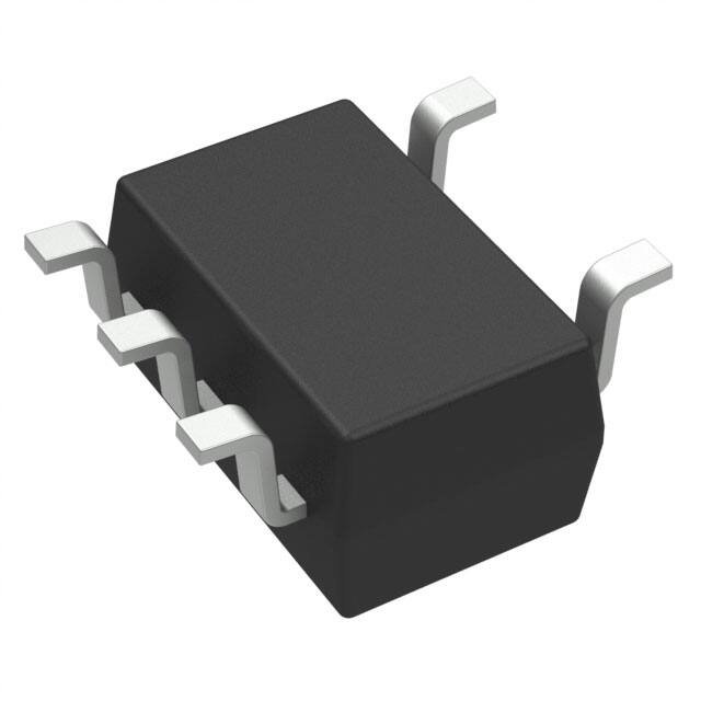
NCS2252. Both options are offered in TSOP−5 (SOT23−5) and
SC−88A (SC70−5) packages. Automotive qualified devices are also
available, denoted by the NCV prefix.
5
•
SCALE 2:1
TSOP−5
(SOT23−5)
CASE 483
SC−88A
(SC70−5)
CASE 419A−02
MARKING DIAGRAMS
Features
•
•
•
•
•
•
•
1
SCALE 2:1
Propagation Delay: 50 ns with 100 mV Overdrive
Rail−to−rail Input: VSS − 200 mV to VDD + 200 mV
Supply Voltage: 1.8 V to 5.5 V
Supply Current: 150 μA Typical at 5 V Supply
Available with Push−pull or Open Drain Output
Packages: TSOP−5 (SOT23−5) and SC−88A (SC70−5)
NCV Prefix for Automotive and Other Applications Requiring
Unique Site and Control Change Requirements; AEC−Q100
Qualified and PPAP Capable
These Devices are Pb−free, Halogen Free/BFR Free and are RoHS
Compliant
5
XX AYWG
G
XX MG
G
1
XX
A
Y
W
M
G
= Specific Device Code
= Assembly Location
= Year
= Work Week
= Date Code
= Pb−Free Package
(Note: Microdot may be in either location)
Applications
•
•
•
•
•
Voltage Threshold Detector
Zero−crossing Detectors
High−speed Sampling Circuits
Logic Level Shifting / Translation
Clock and Data Signal Restoration
PIN DIAGRAM
End Products
•
•
•
•
•
Automotive
Lighting
Smartphones, cell phones
Portable and battery−powered systems
Power supplies
© Semiconductor Components Industries, LLC, 2011
June, 2018 − Rev. 5
OUT
1
VSS
2
IN+
3
5
VDD
4
IN−
TSOP−5 (SOT23−5) and
SC−88A (SC70−5) pinout
ORDERING INFORMATION
See detailed ordering and shipping information on page 2 of
this data sheet.
1
Publication Order Number:
NCS2250/D
�NCS2250, NCV2250, NCS2252, NCV2252
Table 1. ORDERING INFORMATION
Automotive
Output
Device (Note 1)
Package
Marking
Shipping †
No
Push−Pull
NCS2250SQ2T2G
SC−88A (SC70−5)
5C
3000 / Tape & Reel
NCS2250SN2T1G
TSOP−5 (SOT23−5)
5A
3000 / Tape & Reel
NCS2252SQ2T2G
SC−88A (SC70−5)
5F
3000 / Tape & Reel
NCS2252SN2T1G
TSOP−5 (SOT23−5)
5D
3000 / Tape & Reel
Push−Pull
NCV2250SQ2T2G
SC−88A (SC70−5)
5C
3000 / Tape & Reel
NCV2250SN2T1G
TSOP−5 (SOT23−5)
5A
3000 / Tape & Reel
Open Drain
NCV2252SQ2T2G
SC−88A (SC70−5)
5F
3000 / Tape & Reel
NCV2252SN2T1G
TSOP−5 (SOT23−5)
5D
3000 / Tape & Reel
Open Drain
Yes
†For information on tape and reel specifications, including part orientation and tape sizes, please refer to our Tape and Reel Packaging
Specification Brochure, BRD8011/D.
1. Contact local sales office for more information.
Table 2. PIN DESCRIPTION
Name
Type
VDD
Power
Positive supply pin. Connect to positive rail. A bypass capacitor of at least 0.1 μF is
recommended as close as possible to the VDD pin
VSS
Power
Negative supply pin. Connect to ground or negative rail. If not connected to ground,
a bypass capacitor of at least 0.1 μF is recommended as close as possible to the VSS pin
OUT
Output
Output pin. NCS2250 has a complementary push−pull output stage. NCS2252 has an open
drain output stage which requires an external pull−up resistor
IN−
Input
Inverting input
IN+
Input
Non−inverting input
Description
www.onsemi.com
2
�NCS2250, NCV2250, NCS2252, NCV2252
Table 3. ABSOLUTE MAXIMUM RATINGS (Note 2)
Rating
Symbol
Value
Units
Supply Voltage Range (VDD − VSS)
VS
0 to 6
V
Input Voltage Range
VIN
VSS − 0.3 to VDD + 0.3
V
Output Voltage Range
VO
VSS − 0.3 to VDD + 0.3
V
Output Short Circuit Current (Note 3)
ISC
Continuous
mA
TJ(max)
+150
°C
Storage Temperature Range
Tstg
−65 to +150
°C
ESD Capability (Note 5)
Human Body Model
Machine Model
HBM
MM
2000
50
ILU
100
MSL
Level 1
Maximum Junction Temperature (Note 4)
V
Latch−up Current (Note 6)
Moisture Sensitivity Level (Note 7)
mA
Stresses exceeding those listed in the Maximum Ratings table may damage the device. If any of these limits are exceeded, device functionality
should not be assumed, damage may occur and reliability may be affected.
2. Refer to ELECTRICAL CHARACTERISTICS and APPLICATION INFORMATION for Safe Operating Area.
3. Applies to both single−supply and split−supply operation. Continuous short circuit operation at elevated ambient temperature can result in
exceeding the maximum allowed junction temperature of 150°C. Output currents in excess of ±50 mA over long term may adversely affect
reliability.
4. See APPLICATION INFORMATION for Safe Operating Area.
5. This device series incorporates ESD protection and is tested by the following methods:
− ESD Human Body Model tested per JEDEC standard JESD22−A114 (AEC−Q100−002)
− ESD Machine Model tested per JEDEC standard JESD22−A115 (AEC−Q100−003)
6. Latch−up Current per JEDEC standard JESD78.
7. Moisture Sensitivity Level tested per IPC/JEDEC standard J−ST−020A.
Table 4. THERMAL INFORMATION
Parameter
Symbol
Package
Single Layer Board
(Note 8)
Units
Junction−to−Ambient
Thermal Resistance
qJA
TSOP−5 (SOT23−5)
150
°C/W
SC−88A (SC70−5)
162
8. Values based on a single layer 1S standard PCB with 1.0 oz copper and a 50 mm2 copper area.
Table 5. OPERATING RANGES (Note 9)
Parameter
Symbol
Min
Max
Units
Power Supply Voltage
VS
1.8
5.5
V
Input Common Mode Voltage Range
VCM
VSS – 0.2
VDD + 0.2
V
Ambient Temperature
TA
−40
125
°C
9. See APPLICATION INFORMATION for Safe Operating Area.
www.onsemi.com
3
�NCS2250, NCV2250, NCS2252, NCV2252
Table 6. ELECTRICAL CHARACTERISTICS AT 5 V SUPPLY
Typical values are referenced to TA = 25°C, VDD = 5 V, VSS = 0 V, VCM = mid−supply, CL = 50 pF, unless otherwise noted. NCS2252 is
connected to RPULL−UP = 10 kΩ to VDD, unless otherwise noted. Boldface numbers apply from TA = −40°C to 125°C (Notes 10, 11)
Parameter
Test Conditions
Symbol
No load
IDD
Min
Typ
Max
Units
150
200
μA
SUPPLY CHARACTERISTICS
Quiescent Supply Current
250
Power Supply Rejection Ratio
PSRR
dB
88
62.5
INPUT CHARACTERISTICS
Input Offset Voltage
VOS
0.5
IIB
20
6
mV
6
Input Bias Current
(Note 11)
pA
1000
Input Offset Current
(Note 11)
IOS
pA
20
1000
Common Mode Rejection Ratio
CMRR
81
dB
CIN
3.8
pF
VOH
VDD – 0.1
V
V
59
Input Capacitance
OUTPUT CHARACTERISTICS
Output Voltage High
NCS2250, IOUT = 4 mA
VDD – 0.3
Output Voltage Low
IOUT = 4 mA
VOL
VSS + 0.09
NCS2250, Sourcing
IO
48
VSS + 0.3
Output Current Capability
Sinking
Output Leakage Current
mA
52
NCS2252, VS = 5.5 V
ILEAK
1
nA
Output Rise Time
NCS2250, 10% to 90%, VOD = 100 mV
trise
4
ns
Output Fall Time
NCS2250, 90% to 10%, VOD = 100 mV
tfall
4
ns
NCS2252, 90% to 10%, VOD = 100 mV
Propagation Delay (Note 11)
NCS2250
NCS2252
(Note 12)
VOD = 100 mV
5.5
tpLH, tpHL
VOD = 50 mV
60
VOD = 20 mV
90
VOD = 100 mV
tpHL
VOD = 50 mV
ns
64
ns
90
tSKEW
VOD = 100 mV, CL = 50 pF
50
64
60
VOD = 20 mV
Propagation Delay Skew
(NCS2250)
50
6
VOD = 50 mV, CL = 50 pF
2
VOD = 20 mV, CL = 50 pF
1
ns
10. Refer to ABSOLUTE MAXIMUM RATINGS and APPLICATION INFORMATION for Safe Operating Area.
11. Performance guaranteed over the indicated operating temperature range by design and/or characterization.
12. Typical values are provided for NCS2252 output high−to−low propagation delay. NCS2252 is an open drain comparator. Output low−to−high
propagation delay is a function of the RC time constant, which is dependent on the pull−up resistor.
www.onsemi.com
4
�NCS2250, NCV2250, NCS2252, NCV2252
Table 7. ELECTRICAL CHARACTERISTICS AT 1.8 V SUPPLY
Typical values are referenced to TA = 25°C, VDD = 1.8 V, VSS = 0 V, VCM = mid−supply, CL = 50 pF, unless otherwise noted. NCS2252 is
connected to RPULL−UP = 10 kΩ to VDD, unless otherwise noted. Boldface numbers apply from TA = −40°C to 125°C (Notes 13, 14)
Parameter
Test Conditions
Symbol
No load
IDD
Min
Typ
Max
Units
145
200
μA
SUPPLY CHARACTERISTICS
Quiescent Supply Current
250
Power Supply Rejection Ratio
PSRR
dB
82
62.5
INPUT CHARACTERISTICS
Input Offset Voltage
VOS
0.5
IIB
20
6
mV
6
Input Bias Current
(Note 14)
pA
1000
Input Offset Current
(Note 14)
IOS
pA
20
1000
Common Mode Rejection Ratio
CMRR
76
dB
CIN
4.4
pF
VOH
VDD – 0.14
V
V
55
Input Capacitance
OUTPUT CHARACTERISTICS
Output Voltage High
NCS2250, IOUT = 4 mA
VDD – 0.3
Output Voltage Low
IOUT = 4 mA
VOL
VSS + 0.12
NCS2250, Sourcing
IO
25
VSS + 0.3
Output Current Capability
Sinking
Output Leakage Current
mA
42
NCS2252, VS = 5.5 V
ILEAK
1
nA
Output Rise Time
NCS2250, 10% to 90%, VOD = 100 mV
trise
7
ns
Output Fall Time
NCS2250, 90% to 10%, VOD = 100 mV
tfall
6
ns
tpLH, tpHL
56
NCS2252, 90% to 10%, VOD = 100 mV
Propagation Delay (Note 14)
NCS2250
NCS2252
(Note 15)
VOD = 100 mV
7
VOD = 50 mV
71
VOD = 20 mV
106
VOD = 100 mV
tpHL
VOD = 50 mV
68
ns
106
tSKEW
VOD = 100 mV, CL = 50 pF
ns
71
VOD = 20 mV
Propagation Delay Skew
(NCS2250)
56
68
5
VOD = 50 mV, CL = 50 pF
2
VOD = 20 mV, CL = 50 pF
1
13. Refer to ABSOLUTE MAXIMUM RATINGS and APPLICATION INFORMATION for Safe Operating Area.
14. Performance guaranteed over the indicated operating temperature range by design and/or characterization.
15. Typical values are provided for NCS2252 output high−to−low propagation delay. NCS2252 is an open drain comparator.
Output low−to−high propagation delay is a function of the RC time constant, which is dependent on the pull−up resistor.
www.onsemi.com
5
ns
�NCS2250, NCV2250, NCS2252, NCV2252
GRAPHS
Typical performance at TA = 25°C, unless otherwise noted.
0.2
VS = 5 V
CL = 50 pF
0.15
5
0.25
5
4
0.2
4
3
0.15
2
0.1
1
0.05
1
0
0
3
Input
0
0
20 mV
50 mV
−0.05
−1
100 mV
−0.1
−0.15 INPUT
OUTPUT
−0.25
−25
−0.1
−3
−0.15
25
50
75
100
125
150
175
−1
−2
Input
−0.25
−25
200
50 mV
25
50
Time (ns)
75
100
125
150
175
−5
200
Time (ns)
Figure 1. Transient Response at 5 V Supply
with Varying Input Overdrive Voltages
0.3
Figure 2. Transient Response at 5 V Supply
with Varying Input Overdrive Voltages
1.5
0.15
1.5
INPUT
0.2
VS = 1.8 V
1.0
0.1
0.5
0.05
OUTPUT
1.0
Input
0
0.0
20 mV
50 mV
−0.1
0
0.5
Input
0.0
20 mV
50 mV
−0.05
−0.5
100 mV
VS = 1.8 V
CL = 50 pF
NCS2250
Input (V)
0.1
Output (V)
CL = 50 pF
Input (V)
−4
100 mV
NCS2250
0
−3
20 mV
VS = 5 V
CL = 50 pF
−0.2
−5
0
−0.05
−2
−4
2
OUTPUT
Output (V)
−0.2
Input (V)
Input (V)
0.05
Output (V)
INPUT
0.1
Output (V)
0.25
−0.5
100 mV
INPUT
−0.2
−0.1
−1.0
−1.0
OUTPUT
−0.3
−0.15
−1.5
−25
0
25
50
75
100
125
150
175
−1.5
−25
200
0
25
50
Time (ns)
75
100
125
150
200
Time (ns)
Figure 3. Transient Response at 1.8 V Supply
with Varying Input Overdrive Voltages
Figure 4. Transient Response at 1.8 V Supply
with Varying Input Overdrive Voltages
160
160
Vs =Vs1.8
V V
= 1.8
Vs
Vs = 1.8
1.8 V
V
140
140
Vs = 3 V
Vs =
= 55 V
V
Vs
120
Propagation Delay (ns)
Propagation Dleay (ns)
175
100
80
60
40
Output high−to−low
20
Vs =Vs3 =V 3 V
Vs =Vs5 =V 5 V
120
100
80
60
40
20
Output low−to−high
CL = 50 pF
CL = 50 pF
0
0
0
20
40
60
80
0
100
Input Overdrive Voltage (mV)
20
40
60
80
100
Input Overdrive Voltage (mV)
Figure 5. Output High−to−Low Propagation Delay
vs. Input Overdrive Voltage
Figure 6. Output Low−to−High Propagation Delay
vs. Input Overdrive Voltage
www.onsemi.com
6
�NCS2250, NCV2250, NCS2252, NCV2252
GRAPHS (continued)
Typical performance at TA = 25°C, unless otherwise noted.
140
130
140
Vs = 1.8 V
Output high−to−low
20 mV overdrive
130
Vs = 5 V
120
Propagation dleay (ns)
Propagation Delay (ns)
120
Vs = 3 V
110
100
90
80
70
60
Vs = 5 V
110
100
90
80
70
50
10
20
30
40
50
60
70
80
90
100
10
20
30
Load Capacitance (pF)
40
50
60
70
80
90
100
Load Capacitance (pF)
Figure 7. Output High−to−Low Propagation Delay
vs. Load Capacitance
Figure 8. Output Low−to−High Propagation Delay
vs. Load Capacitance
20
20
IIB+
IIB+
15
15
IIB−
10
IIB−
10
Vs = 1.8 V
Input Current (pA)
Input Current (pA)
Vs = 3 V
20 mV overdrive
NCS2250
60
50
T = 25°C
5
0
−5
−10
Vs = 5 V
5
T = 25°C
0
−5
−10
−15
−15
−20
−0.2
−20
0
0.2
0.4
0.6
0.8
1
1.2
1.4
1.6
1.8
2
−0.2
0.4
1
Common Mode Voltage (V)
1.6
2.2
2.8
3.4
4
4.6
5.2
Common Mode Voltage (V)
Figure 9. Input Current vs. Common Mode
Voltage at 1.8 V Supply
Figure 10. Input Current vs. Common Mode
Voltage at 5 V Supply
225
225
IIB−
200
175
IOS
175
150
Vs = 1.8 V
150
125
100
75
50
50
0
−25
−25
−50
−50
−50
25
50
75
100
Vs = 5 V
75
25
0
IOS
100
0
−25
IIB+
125
25
−50
IIB−
200
IIB+
Input Current (pA)
Input Current (pA)
Vs = 1.8 V
Output low−to−high
125
−25
Temperature (°C)
0
25
50
75
100
125
Temperature (°C)
Figure 11. Input Current vs. Temperature
at 1.8 V Supply
Figure 12. Input Current vs. Temperature
at 5 V Supply
www.onsemi.com
7
�NCS2250, NCV2250, NCS2252, NCV2252
GRAPHS (continued)
Typical performance at TA = 25°C, unless otherwise noted.
1
1
Vs = 5 V
0.9
Vs = 1.8 V
0.7
Vs = 1.8 V
0.8
NCS2250
0.7
VOL−VSS (V)
VDD−VOH (V)
0.8
Vs = 5 V
0.9
0.6
0.5
0.4
0.3
0.6
0.5
0.4
0.3
0.2
0.2
0.1
0.1
0
0
0
5
10
15
20
25
30
35
40
0
10
Output Current (mA)
Figure 13. Output Voltage High (Relative to VDD)
vs. Output Current
30
40
50
Figure 14. Output Voltage Low (Relative to VSS)
vs. Output Current
80
180
Vs = 1.8 V
SINKING
170
60
Vs = 5 V
160
40
20
Vs = 1.8 V
0
Vs = 1.8 V
Supply Current (μA)
Output Current Capability (mA)
20
Output Current (mA)
Vs = 5 V
Vs = 5 V
−20
SOURCING (NCS2250)
140
130
120
110
−40
100
−60
−50
150
−25
0
25
50
75
100
−50
125
Temperature (°C)
−25
0
25
50
75
100
125
Temperature (°C)
Figure 15. Output Current Capability vs. Temperature
Figure 16. Supply Current vs. Temperature
www.onsemi.com
8
�NCS2250, NCV2250, NCS2252, NCV2252
APPLICATION INFORMATION
Input Stage
to provide sourcing current, the timing of the output
low−to−high transition is determined by the RC time
constant of the pull−up resistor and the load capacitance.
The NCS2250 and NCS2252 have rail−to−rail inputs. The
input common mode voltage range of these comparators
extend 200 mV beyond the rails, allowing voltage sensing
at ground or at the supply voltage.
Hysteresis
When the inputs are near the same voltage, slight voltage
fluctuations due to noise can cause the output to oscillate
between high and low states. If noise−induced switching
behavior is observed at the output, hysteresis should be
added through an external resistor network. This is
particularly the case for NCS2250, as sustained output
oscillations causing increased supply current will result in
elevated junction temperature.
Hysteresis can be added to the circuit by adding one or two
external resistors depending on whether an inverting or
non−inverting configuration is needed. Figure 17 shows the
inverting configuration. In this configuration, the output
voltage adjusts the threshold at the IN+ pin.
Output Stage
The NCS2250 has a complementary, push−pull output
stage. When the output transitions between high and low
states, a low resistance path is created between the positive
and negative supply rails, temporarily increasing the supply
current during the transition.
The NCS2252 has an open−drain output stage. This
allows the output to be connected through a pull−up resistor
to another supply voltage for applications where level
translation or level shifting is needed. The output resistor
can be connected to voltages below VDD or up to VDD + 0.3
V. Since the NCS2252 relies on an external pull−up resistor
RF
R1
+
NCS2250
R2
VIN
−
Figure 17. Comparator with Hysteresis, Inverting Configuration
For the inverting configuration, the value of the
high−level input voltage which triggers the output to switch
from high to low is given by the following equation:
V IN_high +
R1
R1
RF ) R1
RF
R2 ) R2
RF
V DD
The value of the low−level input voltage which triggers
the output to switch from low to high is given by the
following equation:
V IN_low +
(eq. 1)
www.onsemi.com
9
R1
RF ) R1 R2
R1
RF ) R1
R2 ) R2
RF
V DD
(eq. 2)
�NCS2250, NCV2250, NCS2252, NCV2252
Figure 18 shows the non−inverting configuration. For the
non−inverting configuration, the threshold Vth set by R1 and
R2 is fixed. The output adjusts the input signal on IN+.
RF
RIN
VIN
+
R1
NCS2250
−
R2
Figure 18. Comparator with Hysteresis, Non−Inverting
Configuration
Layout Techniques
The value of the high−level input voltage which triggers
the output to switch from low to high is given by the
following equation:
V IN_high +
V th
(R IN ) R F)
RF
High speed layout techniques are recommended for the
best performance.
Bypass capacitors of at least 0.1 mF must be placed as
close as possible to supply pins.
The traces on the input pins should be short to minimize
any noise on the high impedance inputs. In general, shorter
traces will reduce parasitic capacitance, inductance, and
resistance.
Identify and keep sensitive traces away from possible
noise sources such as clocks. Crosstalk can be reduced by
increasing the distance between traces. Do not let traces run
parallel for long distances. Take advantage of routing layers
to separate traces that would otherwise run parallel. Ground
or DC voltage supplies can be used to separate a sensitive
trace from a noise source.
Avoid floating nodes as these will pick up noise.
(eq. 3)
The value of the low−level input voltage which triggers
the output to switch from high to low is given by the
following equation:
V IN_low +
V th
(R IN ) R F) * R IN
RF
V DD
(eq. 4)
Power dissipation
The absolute maximum junction temperature is 150°C.
The junction temperature can be calculated using the power
dissipation P, thermal resistance qJA , and ambient
temperature TA .
T J + q JA
P ) TA
(eq. 5)
www.onsemi.com
10
�NCS2250, NCV2250, NCS2252, NCV2252
PACKAGE DIMENSIONS
SC−88A (SC−70−5/SOT−353)
CASE 419A−02
ISSUE L
A
NOTES:
1. DIMENSIONING AND TOLERANCING
PER ANSI Y14.5M, 1982.
2. CONTROLLING DIMENSION: INCH.
3. 419A−01 OBSOLETE. NEW STANDARD
419A−02.
4. DIMENSIONS A AND B DO NOT INCLUDE
MOLD FLASH, PROTRUSIONS, OR GATE
BURRS.
G
5
4
−B−
S
1
2
DIM
A
B
C
D
G
H
J
K
N
S
3
D 5 PL
0.2 (0.008)
M
B
M
N
J
C
K
H
SOLDER FOOTPRINT
0.50
0.0197
0.65
0.025
0.65
0.025
0.40
0.0157
1.9
0.0748
SCALE 20:1
www.onsemi.com
11
mm Ǔ
ǒinches
INCHES
MIN
MAX
0.071
0.087
0.045
0.053
0.031
0.043
0.004
0.012
0.026 BSC
--0.004
0.004
0.010
0.004
0.012
0.008 REF
0.079
0.087
MILLIMETERS
MIN
MAX
1.80
2.20
1.15
1.35
0.80
1.10
0.10
0.30
0.65 BSC
--0.10
0.10
0.25
0.10
0.30
0.20 REF
2.00
2.20
�NCS2250, NCV2250, NCS2252, NCV2252
TSOP−5 / (SOT23−5)
CASE 483
ISSUE M
NOTE 5
2X
NOTES:
1. DIMENSIONING AND TOLERANCING PER ASME
Y14.5M, 1994.
2. CONTROLLING DIMENSION: MILLIMETERS.
3. MAXIMUM LEAD THICKNESS INCLUDES LEAD FINISH
THICKNESS. MINIMUM LEAD THICKNESS IS THE
MINIMUM THICKNESS OF BASE MATERIAL.
4. DIMENSIONS A AND B DO NOT INCLUDE MOLD
FLASH, PROTRUSIONS, OR GATE BURRS. MOLD
FLASH, PROTRUSIONS, OR GATE BURRS SHALL NOT
EXCEED 0.15 PER SIDE. DIMENSION A.
5. OPTIONAL CONSTRUCTION: AN ADDITIONAL
TRIMMED LEAD IS ALLOWED IN THIS LOCATION.
TRIMMED LEAD NOT TO EXTEND MORE THAN 0.2
FROM BODY.
D 5X
0.20 C A B
0.10 T
M
2X
0.20 T
B
5
1
4
2
S
3
K
B
DETAIL Z
G
A
A
TOP VIEW
DIM
A
B
C
D
G
H
J
K
M
S
DETAIL Z
J
C
0.05
H
SIDE VIEW
C
SEATING
PLANE
END VIEW
MILLIMETERS
MIN
MAX
2.85
3.15
1.35
1.65
0.90
1.10
0.25
0.50
0.95 BSC
0.01
0.10
0.10
0.26
0.20
0.60
0_
10 _
2.50
3.00
SOLDERING FOOTPRINT*
0.95
0.037
1.9
0.074
2.4
0.094
1.0
0.039
0.7
0.028
SCALE 10:1
mm Ǔ
ǒinches
*For additional information on our Pb−Free strategy and soldering
details, please download the ON Semiconductor Soldering and
Mounting Techniques Reference Manual, SOLDERRM/D.
ON Semiconductor and
are trademarks of Semiconductor Components Industries, LLC dba ON Semiconductor or its subsidiaries in the United States and/or other countries.
ON Semiconductor owns the rights to a number of patents, trademarks, copyrights, trade secrets, and other intellectual property. A listing of ON Semiconductor’s product/patent
coverage may be accessed at www.onsemi.com/site/pdf/Patent−Marking.pdf. ON Semiconductor reserves the right to make changes without further notice to any products herein.
ON Semiconductor makes no warranty, representation or guarantee regarding the suitability of its products for any particular purpose, nor does ON Semiconductor assume any liability
arising out of the application or use of any product or circuit, and specifically disclaims any and all liability, including without limitation special, consequential or incidental damages.
Buyer is responsible for its products and applications using ON Semiconductor products, including compliance with all laws, regulations and safety requirements or standards,
regardless of any support or applications information provided by ON Semiconductor. “Typical” parameters which may be provided in ON Semiconductor data sheets and/or
specifications can and do vary in different applications and actual performance may vary over time. All operating parameters, including “Typicals” must be validated for each customer
application by customer’s technical experts. ON Semiconductor does not convey any license under its patent rights nor the rights of others. ON Semiconductor products are not
designed, intended, or authorized for use as a critical component in life support systems or any FDA Class 3 medical devices or medical devices with a same or similar classification
in a foreign jurisdiction or any devices intended for implantation in the human body. Should Buyer purchase or use ON Semiconductor products for any such unintended or unauthorized
application, Buyer shall indemnify and hold ON Semiconductor and its officers, employees, subsidiaries, affiliates, and distributors harmless against all claims, costs, damages, and
expenses, and reasonable attorney fees arising out of, directly or indirectly, any claim of personal injury or death associated with such unintended or unauthorized use, even if such
claim alleges that ON Semiconductor was negligent regarding the design or manufacture of the part. ON Semiconductor is an Equal Opportunity/Affirmative Action Employer. This
literature is subject to all applicable copyright laws and is not for resale in any manner.
PUBLICATION ORDERING INFORMATION
LITERATURE FULFILLMENT:
Literature Distribution Center for ON Semiconductor
19521 E. 32nd Pkwy, Aurora, Colorado 80011 USA
Phone: 303−675−2175 or 800−344−3860 Toll Free USA/Canada
Fax: 303−675−2176 or 800−344−3867 Toll Free USA/Canada
Email: orderlit@onsemi.com
◊
N. American Technical Support: 800−282−9855 Toll Free
USA/Canada
Europe, Middle East and Africa Technical Support:
Phone: 421 33 790 2910
www.onsemi.com
12
ON Semiconductor Website: www.onsemi.com
Order Literature: http://www.onsemi.com/orderlit
For additional information, please contact your local
Sales Representative
NSC2250/D
�