NCV4250-2C
Low Dropout Voltage
Tracking Regulator
The NCV4250−2C is a monolithic integrated low dropout tracking
voltage regulator designed to provide a buffered output voltage that
closely tracks the reference input voltage. The part can be used in
automotive applications with remote sensors or any situation where
it is necessary to isolate the output of the other regulator. The
NCV4250−2C also enables the user to bestow a quick upgrade to
their module when added current is needed and the existing regulator
cannot provide.
www.onsemi.com
MARKING
DIAGRAM
5
TSOP−5
CASE 483
Features
•
•
•
•
•
•
•
•
5
Up to 50 mA Source Capability
Low Output Tracking Tolerance
Low Dropout (typ. 120 mV @ 10 mA)
Low Quiescent Current in Stand−by Mode
Wide Input Voltage Operating Range
Protection Features:
♦ Current Limitation
♦ Thermal Shutdown
♦ Reverse Input Voltage and Reverse Bias Voltage
AEC−Q100 Grade 1 Qualified and PPAP Capable
This is a Pb−Free Device
425AYWG
G
1
1
425
A
Y
W
G
= Specific Device Code
= Assembly Location
= Year
= Work Week
= Pb−Free Package
(Note: Microdot may be in either location)
PIN CONNECTIONS
Typical Applications
• Off the Module Loads (e.g. Sensors Power Supply)
EN/REF
1
GND
2
Vin
3
5
GND
4
Vout
(Top View)
ORDERING INFORMATION
See detailed ordering and shipping information on page 9 of
this data sheet.
Supply
Cin
Reference
Vout
Vin
Output (e.g. Sensor Supply)
Cout
NCV4250−2C
EN/REF
GND
Figure 1. Applications Circuit
© Semiconductor Components Industries, LLC, 2016
October, 2017 − Rev. 0
1
Publication Order Number:
NCV4250−2C/D
�NCV4250−2C
Vout
Vin
EN/REF
BIAS
CURRENT LIMIT
SATURATION PROTECTION
THERMAL
SHUTDOWN
−
+
GND
EN/REF
Figure 2. Block Diagram
PIN FUNCTION DESCRIPTION
Pin No.
TSOP−5
Pin Name
1
EN/REF
2
GND
3
Vin
Positive Power Supply Input. Connect 0.1 mF capacitor to ground.
4
Vout
Tracker Output Voltage. Connect 1 mF capacitor with ESR < 3 W to ground.
5
GND
Power Supply Ground.
Description
Enable / Reference.
Connect the reference to this pin. A low signal disables the IC; a high signal switches it on.
The reference voltage can be connected directly or by a voltage divider for lower output voltages.
Power Supply Ground.
ABSOLUTE MAXIMUM RATINGS
Rating
Symbol
Input Voltage DC (Note 1)
DC
Vin
Output Voltage
Vout
Min
Max
−42
45
−1
40
−0.3
40
Unit
V
V
Enable / Reference Input Voltage DC
DC
VEN/REF
Maximum Junction Temperature
TJ(max)
−40
150
°C
TSTG
−55
150
°C
Storage Temperature
V
Stresses exceeding those listed in the Maximum Ratings table may damage the device. If any of these limits are exceeded, device functionality
should not be assumed, damage may occur and reliability may be affected.
1. Refer to ELECTRICAL CHARACTERISTICS and APPLICATION INFORMATION for Safe Operating Area.
ESD CAPABILITY (Note 2)
Rating
ESD Capability, Human Body Model
Symbol
Min
Max
Unit
ESDHBM
−3
3
kV
2. This device series incorporates ESD protection and is tested by the following methods:
ESD Human Body Model tested per AEC−Q100−002 (JS−001−2010)
Field Induced Charge Device Model ESD characterization is not performed on plastic molded packages with body sizes < 50 mm2 due to the
inability of a small package body to acquire and retain enough charge to meet the minimum CDM discharge current waveform characteristic
defined in JEDEC JS−002−2014.
www.onsemi.com
2
�NCV4250−2C
LEAD SOLDERING TEMPERATURE AND MSL (Note 3)
Rating
Symbol
Moisture Sensitivity Level
Min
MSL
Max
1
Unit
−
3. For more information, please refer to our Soldering and Mounting Techniques Reference Manual, SOLDERRM/D
THERMAL CHARACTERISTICS
Rating
Symbol
Value
RθJA
RYJL2
136
49
Unit
°C/W
Thermal Characteristics, TSOP−5
Thermal Resistance, Junction−to−Air (Note 4)
Thermal Resistance, Junction−to−Lead 2 (Note 4)
4. Values based on copper area of 645 mm2 (or 1 in2) of 1 oz copper thickness and FR4 PCB substrate.
RECOMMENDED OPERATING RANGES
Rating
Input Voltage
Enable / Reference Input Voltage
Junction Temperature
Symbol
Min
Max
Unit
Vin
4
40
V
VEN/REF
2.5
36
V
TJ
−40
150
°C
Functional operation above the stresses listed in the Recommended Operating Ranges is not implied. Extended exposure to stresses beyond the
Recommended Operating Ranges limits may affect device reliability.
www.onsemi.com
3
�NCV4250−2C
ELECTRICAL CHARACTERISTICS
Vin = 13.5 V, VEN/REF > = 2.5 V, Cin = 0.1 mF, Cout = 1 mF, for typical values TJ = 25°C, for min/max values TJ = −40°C to 150°C; unless
otherwise noted. (Note 5)
Parameter
Test Conditions
Symbol
Min
Typ
Max
Unit
Output Voltage Tracking Accuracy
Vin = 6 V to 16 V, Iout = 1 mA to 10 mA
nVout
−5
−
5
mV
Output Voltage Tracking Accuracy
Vin = 6 V to 28 V, Iout = 1 mA to 50 mA
nVout
−25
−
25
mV
Output Voltage Tracking Accuracy
Vin = 6 V to 40 V, Iout = 1 mA to 10 mA
nVout
−25
−
25
mV
Vin = 6 V to 40 V, Iout = 10 mA
Regline
−10
−
10
mV
REGULATOR OUTPUT
Line Regulation
Load Regulation
Dropout Voltage (Note 6)
Iout = 1 mA to 30 mA
Regload
−15
−
15
mV
Iout = 10 mA, VEN/REF > 4 V
VDO
−
120
300
mV
VEN/REF
很抱歉,暂时无法提供与“NCV4250-2CSNT1G”相匹配的价格&库存,您可以联系我们找货
免费人工找货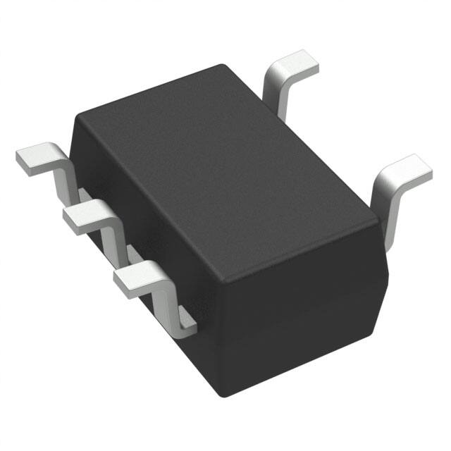


 工商网监
湘ICP备2023018690号
工商网监
湘ICP备2023018690号
