NCV4266
Regulator with Enable,
150 mA, Low-Dropout
Voltage
The NCV4266 is a 150 mA output current integrated low dropout
regulator family designed for use in harsh automotive environments.
It includes wide operating temperature and input voltage ranges. The
device is offered with fixed voltage versions of 3.3 V and 5.0 V
available in 2% output voltage accuracy. It has a high peak input
voltage tolerance and reverse input voltage protection. It also
provides overcurrent protection, overtemperature protection and
enable function for control of the state of the output voltage. The
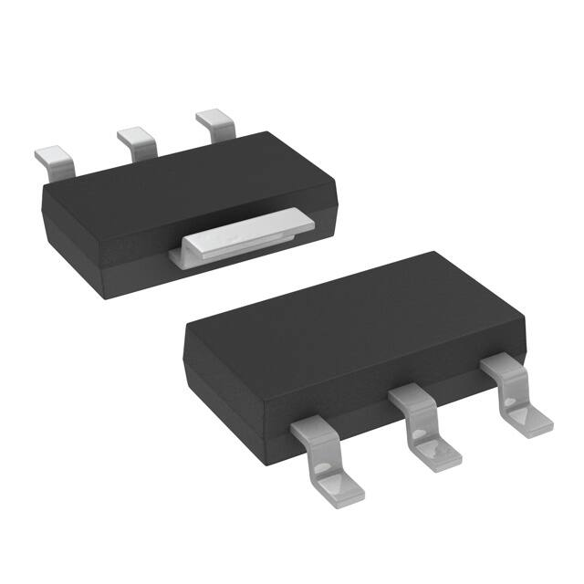
NCV4266 is available in SOT−223 surface mount package. The
output is stable over a wide output capacitance and ESR range. The
NCV4266 has improved startup behavior during input voltage
transients.
www.onsemi.com
SOT−223
ST SUFFIX
CASE 318E
MARKING DIAGRAM
Features
•
•
•
•
•
•
•
•
AYW
4266xG
G
3.3 V and 5.0 V Output Voltage
150 mA Output Current
500 mV (max) Dropout Voltage
Enable Input
Very Low Current Consumption
Fault Protection
♦ +45 V Peak Transient Voltage
♦ −42 V Reverse Voltage
♦ Short Circuit
♦ Thermal Overload
NCV Prefix for Automotive and Other Applications Requiring
Unique Site and Control Change Requirements; AEC−Q100
Qualified and PPAP Capable
These are Pb−Free Devices
I
1
A
Y
W
x
G
= Assembly Location
= Year
= Work Week
= Voltage Option
3.3 V (x = 3)
5.0 V (x = 5)
= Pb−Free Package
(Note: Microdot may be in either location)
ORDERING INFORMATION
See detailed ordering and shipping information in the ordering
information section on page 10 of this data sheet.
Q
Bandgap
Reference
Error
Amplifier
Current Limit and
Saturation Sense
−
+
Thermal
Shutdown
EN
GND
Figure 1. Block Diagram
© Semiconductor Components Industries, LLC, 2012
November, 2018 − Rev. 3
1
Publication Order Number:
NCV4266/D
�NCV4266
PIN FUNCTION DESCRIPTION
Pin No.
Symbol
1
I
2
EN
3
Q
4
GND
Description
Input; Battery Supply Input Voltage.
Enable Input; low level disables the IC.
Output; Bypass with a capacitor to GND.
Ground.
MAXIMUM RATINGS*
Rating
Symbol
Min
Max
Unit
Input Voltage
VI
−42
45
V
Input Peak Transient Voltage
VI
−
45
V
Enable Input Voltage
VEN
−42
45
V
Output Voltage
VQ
−1.0
40
V
Ground Current
Iq
−
100
mA
Input Voltage Operating Range
VI
VQ + 0.5 V or
4.5 (Note 1)
40
V
−
−
4.0
250
−
−
kV
V
Junction Temperature
TJ
−40
150
°C
Storage Temperature
Tstg
−50
150
°C
ESD Susceptibility
(Human Body Model)
(Machine Model)
Stresses exceeding those listed in the Maximum Ratings table may damage the device. If any of these limits are exceeded, device functionality
should not be assumed, damage may occur and reliability may be affected.
*During the voltage range which exceeds the maximum tested voltage of I, operation is assured, but not specified. Wider limits may apply. Thermal
dissipation must be observed closely.
1. Minimum VI = 4.5 V or (VQ + 0.5 V), whichever is higher.
LEAD TEMPERATURE SOLDERING REFLOW AND MSL (Note 2)
Rating
Symbol
Lead Temperature Soldering
Reflow (SMD styles only), Leaded, 60−150 s above 183, 30 s max at peak
Reflow (SMD styles only), Free, 60−150 s above 217, 40 s max at peak
Wave Solder (through hole styles only), 12 sec max
TSLD
Moisture Sensitivity Level
MSL
Min
Max
−
−
−
240
265
310
3
Unit
°C
−
2. Per IPC / JEDEC J−STD−020C.
THERMAL CHARACTERISTICS
Characteristic
Test Conditions (Typical Value)
Unit
Min Pad Board (Note 3)
1, Pad Board (Note 4)
Junction−to−Tab (psi−JL4, yJL4)
15.7
18
C/W
Junction−to−Ambient (RqJA, qJA)
96
77
C/W
3. 1 oz. copper, 0.26 inch2 (168 mm2) copper area, 0.062″ thick FR4.
4. 1 oz. copper, 1.14 inch2 (736 mm2) copper area, 0.062″ thick FR4.
www.onsemi.com
2
�NCV4266
ELECTRICAL CHARACTERISTICS (VI = 13.5 V; −40°C < TJ < 150°C; unless otherwise noted.)
Symbol
Characteristic
Test Conditions
Min
Typ
Max
Unit
4.9
5.0
5.1
V
3.234
3.3
3.366
V
150
200
500
mA
OUTPUT
Output Voltage (5.0 V Version)
VQ
5.0 mA < IQ < 150 mA, 6 V < VI < 28 V
Output Voltage (3.3 V Version)
VQ
5.0 mA < IQ < 150 mA, 4.5 V < VI < 28 V
Output Current Limitation
IQ
VQ = 90% VQTYP
Quiescent Current (Sleep Mode)
Iq = II − IQ
Iq
VEN = 0 V
−
−
10
mA
Quiescent Current, Iq = II − IQ
Iq
IQ = 1.0 mA
−
130
200
mA
Quiescent Current, Iq = II − IQ
Iq
IQ = 150 mA
−
10
15
mA
IQ = 150 mA, VDR = VI − VQ (Note 5)
−
250
500
mV
IQ = 5.0 mA to 150 mA
−
3.0
20
mV
Dropout Voltage (5.0 V Version)
Load Regulation
VDR
DVQ,LO
Line Regulation (5.0 V Version)
DVQ
DVI = 6.0 V to 28 V, IQ = 5.0 mA
−
10
25
mV
Line Regulation (3.3 V Version)
DVQ
DVI = 4.5 V to 28 V, IQ = 5.0 mA
−
10
25
mV
Power Supply Ripple Rejection
PSRR
fr = 100 Hz, Vr = 0.5 VPP
−
70
−
dB
Temperature Output Voltage Drift
dVQ/dT
−
0.5
−
mV/K
−
ENABLE INPUT
Enable Voltage, Output High
VEN
VQ w VQMIN
−
2.3
2.8
V
Enable Voltage, Output Low (Off)
VEN
VQ v 0.1 V
1.8
2.2
−
V
Enable Input Current
IEN
VEN = 5.0 V
5.0
10
20
mA
150
−
210
°C
THERMAL SHUTDOWN
Thermal Shutdown Temperature*
TSD
*Guaranteed by design, not tested in production.
5. Measured when the output voltage VQ has dropped 100 mV from the nominal value obtained at V = 13.5 V.
Input
II
CI1
1.0 mF
I 1
CI2
100 nF
NCV4266
EN
IEN
2
IQ
3 Q
CQ
22 mF
RL
4
GND
Figure 2. Applications Circuit
www.onsemi.com
3
Output
�NCV4266
TYPICAL PERFORMANCE CHARACTERISTICS
100
Unstable Region
CQ = 10 mF − 100 mF
ESR (W)
10
1
Stable Region
0.1
0.01
0
25
50
75
100
125
150
OUTPUT CURRENT (mA)
Figure 3. Output Stability with Output Capacitor ESR
3.5
VI = 13.5 V
RL = 1 kW
VQ, OUTPUT VOLTAGE (V)
VQ, OUTPUT VOLTAGE (V)
5.2
5.1
5.0
4.9
4.8
−40
0
40
80
120
VI = 13.5 V
RL = 660 W
3.4
3.3
3.2
3.1
−40
160
0
TJ, JUNCTION TEMPERATURE (°C)
Figure 4. Output Voltage vs. Junction
Temperature, 5.0 V Version
15
10
5
0
0
5
10
15
20
25
30
VI, INPUT VOLTAGE (V)
120
6
TJ = 25°C
RL = 33 W
20
80
160
Figure 5. Output Voltage vs. Junction
Temperature, 3.3 V Version
Iq, QUIESCENT CURRENT (mA)
Iq, QUIESCENT CURRENT (mA)
25
40
TJ, JUNCTION TEMPERATURE (°C)
35
5
4
3
2
1
0
40
Figure 6. Quiescent Current vs. Input Voltage,
5.0 V Version
TJ = 25°C
RL = 22 W
0
5
10
15
20
25
30
VI, INPUT VOLTAGE (V)
35
Figure 7. Quiescent Current vs. Input Voltage,
3.3 V Version
www.onsemi.com
4
40
�NCV4266
TYPICAL PERFORMANCE CHARACTERISTICS
6
TJ = 25°C
RL = 33 W
5
VQ, OUTPUT VOLTAGE (V)
VQ, OUTPUT VOLTAGE (V)
6
4
3
2
1
0
0
2
4
6
VI, INPUT VOLTAGE (V)
8
4
3
2
1
0
10
TJ = 25°C
RL = 22 W
5
0
2
6.0
1
4.0
0
2.0
0
−2.0
−4.0
−6.0
TJ = 25°C
RL = 6.8 kW
−8.0
−10
−50
−25
0
25
10
−1
−2
−3
−4
−5
TJ = 25°C
RL = 6.8 kW
−6
−7
−50
50
−25
VI, INPUT VOLTAGE (V)
0
25
50
VI, INPUT VOLTAGE (V)
Figure 11. Input Current vs. Input Voltage,
3.3 V Version
Figure 10. Input Current vs. Input Voltage,
5.0 V Version
400
IQ, OUTPUT CURRENT (mA)
300
VDR, DROPOUT VOLTAGE (mV)
8
Figure 9. Output Voltage vs. Input Voltage,
3.3 V Version
II, INPUT CURRENT (mA)
II, INPUT CURRENT (mA)
Figure 8. Output Voltage vs. Input Voltage,
5.0 V Version
4
6
VI, INPUT VOLTAGE (V)
250
TJ = 125°C
200
150
TJ = 25°C
100
50
TJ = 25°C
VQ = 0 V
350
300
250
200
150
100
50
0
0
25
50
75
100
IQ, OUTPUT CURRENT (mA)
125
150
0
0
Figure 12. Dropout Voltage vs. Output Current
(5.0 V Version only)
5
10
15
20
25
30
VI, INPUT VOLTAGE (V)
35
Figure 13. Maximum Output Current vs.
Input Voltage
www.onsemi.com
5
40
�NCV4266
TYPICAL PERFORMANCE CHARACTERISTICS
6
TJ = 25°C
VI = 13.5 V
0.8
Iq, QUIESCENT CURRENT (mA)
Iq, QUIESCENT CURRENT (mA)
1
0.6
0.4
0.2
0
0
5
10
15
20
25
4
3
2
1
0
25
50
75
100
125
IQ, OUTPUT CURRENT (mA)
IQ, OUTPUT CURRENT (mA)
Figure 14. Quiescent Current vs. Output Current
(Low Load), 5.0 V Version
Figure 15. Quiescent Current vs. Output
Current (High Load), 5.0 V Version
6
1
TJ = 25°C
VI = 13.5 V
0.8
Iq, QUIESCENT CURRENT (mA)
Iq, QUIESCENT CURRENT (mA)
5
0
30
TJ = 25°C
VI = 13.5 V
0.6
0.4
0.2
0
0
5
10
15
20
25
TJ = 25°C
VI = 13.5 V
5
4
3
2
1
0
30
0
IQ, OUTPUT CURRENT (mA)
25
50
75
100
125
IQ, OUTPUT CURRENT (mA)
Figure 17. Quiescent Current vs. Output
Current (High Load), 3.3 V Version
Figure 16. Quiescent Current vs. Output Current
(Low Load), 3.3 V Version
www.onsemi.com
6
150
150
�NCV4266
Circuit Description
The NCV4266 is an integrated low dropout regulator that
provides a regulated voltage at 150 mA to the output. It is
enabled with an input to the enable pin. The regulator
voltage is provided by a PNP pass transistor controlled by
an error amplifier with a bandgap reference, which gives it
the lowest possible dropout voltage. The output current
capability is 150 mA, and the base drive quiescent current
is controlled to prevent oversaturation when the input
voltage is low or when the output is overloaded. The
regulator is protected by both current limit and thermal
shutdown. Thermal shutdown occurs above 150°C to
protect the IC during overloads and extreme ambient
temperatures.
transient response and loop stability. The capacitor value
and type should be based on cost, availability, size and
temperature constraints. The aluminum electrolytic
capacitor is the least expensive solution, but, if the circuit
operates at low temperatures (−25°C to −40°C), both the
value and ESR of the capacitor will vary considerably. The
capacitor manufacturer’s data sheet usually provides this
information.
The value for the output capacitor CQ, shown in Figure 2,
should work for most applications; see also Figure 3 for
output stability at various load and Output Capacitor ESR
conditions. Stable region of ESR in Figure 3 shows ESR
values at which the LDO output voltage does not have any
permanent oscillations at any dynamic changes of output
load current. Marginal ESR is the value at which the output
voltage waving is fully damped during four periods after
the load change and no oscillation is further observable.
ESR characteristics were measured with ceramic
capacitors and additional series resistors to emulate ESR.
Low duty cycle pulse load current technique has been used
to maintain junction temperature close to ambient
temperature.
Regulator
The error amplifier compares the reference voltage to a
sample of the output voltage (VQ) and drives the base of a
PNP series pass transistor via a buffer. The reference is a
bandgap design to give it a temperature−stable output.
Saturation control of the PNP is a function of the load
current and input voltage. Oversaturation of the output
power device is prevented, and quiescent current in the
ground pin is minimized. See Figure 2, Test Circuit, for
circuit element nomenclature illustration.
Enable Input
The enable pin is used to turn the regulator on or off. By
holding the pin down to a voltage less than 1.8 V, the output
of the regulator will be turned off. When the voltage on the
enable pin is greater than 2.8 V, the output of the regulator
will be enabled to power its output to the regulated output
voltage. The enable pin may be connected directly to the
input pin to give constant enable to the output regulator.
Regulator Stability Considerations
The input capacitors (CI1 and CI2) are necessary to
stabilize the input impedance to avoid voltage line
influences. Using a resistor of approximately 1.0 W in
series with CI2 can stop potential oscillations caused by
stray inductance and capacitance.
The output capacitor helps determine three main
characteristics of a linear regulator: startup delay, load
www.onsemi.com
7
�NCV4266
Calculating Power Dissipation
in a Single Output Linear Regulator
The maximum power dissipation for a single output
regulator (Figure 18) is:
PD(max) + [VI(max) * VQ(min)] IQ(max)
Heatsinks
A heatsink effectively increases the surface area of the
package to improve the flow of heat away from the IC and
into the surrounding air.
Each material in the heat flow path between the IC and
the outside environment will have a thermal resistance.
Like series electrical resistances, these resistances are
summed to determine the value of RqJA:
(1)
) VI(max)Iq
where
RqJA + RqJC ) RqCS ) RqSA
VI(max)
VQ(min)
IQ(max)
is the maximum input voltage,
is the minimum output voltage,
is the maximum output current for the
application,
Iq
is the quiescent current the regulator
consumes at IQ(max).
Once the value of PD(max) is known, the maximum
permissible value of RqJA can be calculated:
o
T
RqJA + 150 C * A
PD
where
RqJC is the junction−to−case thermal resistance,
RqCS is the case−to−heatsink thermal resistance,
RqSA is the heatsink−to−ambient thermal
resistance.
RqJC appears in the package section of the data sheet.
Like RqJA, it too is a function of package type. RqCS and
RqSA are functions of the package type, heatsink and the
interface between them. These values appear in data sheets
of heatsink manufacturers.
Thermal, mounting, and heatsinking considerations are
discussed in the ON Semiconductor application note
AN1040/D.
(2)
The value of RqJA can then be compared with those in the
package section of the data sheet. Those packages with
RqJA less than the calculated value in Equation 2 will keep
the die temperature below 150°C.
In some cases, none of the packages will be sufficient to
dissipate the heat generated by the IC, and an external
heatsink will be required.
IQ
II
VI
SMART
REGULATOR®
(3)
VQ
} Control
Features
Iq
Figure 18. Single Output Regulator with Key
Performance Parameters Labeled
www.onsemi.com
8
�RqJA, THERMAL RESISTANCE (C°/W)
NCV4266
140
130
120
110
100
90
1 oz
80
70
60
2 oz
0
100
200
300
400
500
COPPER HEAT SPREADER AREA
600
700
(mm2)
Figure 19. RqJA vs. Copper Spreader Area
100
Cu Area 167 mm2
Cu Area 736 mm2
R(t) C°/W
10
1
0.1
0.000001
0.00001
0.0001
0.001
0.01
0.1
TIME (sec)
1
10
100
1000
10
100
1000
Figure 20. Single−Pulse Heating Curves
100
RqJA 736 mm2 C°/W
50% Duty Cycle
20%
10
10%
5%
2%
1
1%
Non−normalized Response
0.1
0.000001
0.00001
0.0001
0.001
0.01
0.1
1
PULSE WIDTH (sec)
Figure 21. Duty Cycle for 1, Spreader Boards
www.onsemi.com
9
�NCV4266
ORDERING INFORMATION
Output Voltage
Package
Shipping†
NCV4266ST33T3G
3.3 V
SOT−223
(Pb−Free)
4000 / Tape & Reel
NCV4266ST50T3G
5.0 V
SOT−223
(Pb−Free)
4000 / Tape & Reel
Device*
†For information on tape and reel specifications, including part orientation and tape sizes, please refer to our Tape and Reel Packaging
Specifications Brochure, BRD8011/D.
*NCV Prefix for Automotive and Other Applications Requiring Unique Site and Control Change Requirements; AEC−Q100 Qualified and PPAP
Capable.
www.onsemi.com
10
�MECHANICAL CASE OUTLINE
PACKAGE DIMENSIONS
SOT−223 (TO−261)
CASE 318E−04
ISSUE R
DATE 02 OCT 2018
SCALE 1:1
q
q
DOCUMENT NUMBER:
DESCRIPTION:
98ASB42680B
SOT−223 (TO−261)
Electronic versions are uncontrolled except when accessed directly from the Document Repository.
Printed versions are uncontrolled except when stamped “CONTROLLED COPY” in red.
PAGE 1 OF 2
ON Semiconductor and
are trademarks of Semiconductor Components Industries, LLC dba ON Semiconductor or its subsidiaries in the United States and/or other countries.
ON Semiconductor reserves the right to make changes without further notice to any products herein. ON Semiconductor makes no warranty, representation or guarantee regarding
the suitability of its products for any particular purpose, nor does ON Semiconductor assume any liability arising out of the application or use of any product or circuit, and specifically
disclaims any and all liability, including without limitation special, consequential or incidental damages. ON Semiconductor does not convey any license under its patent rights nor the
rights of others.
© Semiconductor Components Industries, LLC, 2018
www.onsemi.com
�SOT−223 (TO−261)
CASE 318E−04
ISSUE R
STYLE 1:
PIN 1.
2.
3.
4.
BASE
COLLECTOR
EMITTER
COLLECTOR
STYLE 2:
PIN 1.
2.
3.
4.
ANODE
CATHODE
NC
CATHODE
STYLE 6:
PIN 1.
2.
3.
4.
RETURN
INPUT
OUTPUT
INPUT
STYLE 7:
PIN 1.
2.
3.
4.
ANODE 1
CATHODE
ANODE 2
CATHODE
STYLE 11:
PIN 1. MT 1
2. MT 2
3. GATE
4. MT 2
STYLE 3:
PIN 1.
2.
3.
4.
GATE
DRAIN
SOURCE
DRAIN
STYLE 8:
STYLE 12:
PIN 1. INPUT
2. OUTPUT
3. NC
4. OUTPUT
CANCELLED
DATE 02 OCT 2018
STYLE 4:
PIN 1.
2.
3.
4.
SOURCE
DRAIN
GATE
DRAIN
STYLE 5:
PIN 1.
2.
3.
4.
STYLE 9:
PIN 1.
2.
3.
4.
INPUT
GROUND
LOGIC
GROUND
STYLE 10:
PIN 1. CATHODE
2. ANODE
3. GATE
4. ANODE
DRAIN
GATE
SOURCE
GATE
STYLE 13:
PIN 1. GATE
2. COLLECTOR
3. EMITTER
4. COLLECTOR
GENERIC
MARKING DIAGRAM*
AYW
XXXXXG
G
1
A
= Assembly Location
Y
= Year
W
= Work Week
XXXXX = Specific Device Code
G
= Pb−Free Package
(Note: Microdot may be in either location)
*This information is generic. Please refer to
device data sheet for actual part marking.
Pb−Free indicator, “G” or microdot “G”, may
or may not be present. Some products may
not follow the Generic Marking.
DOCUMENT NUMBER:
DESCRIPTION:
98ASB42680B
SOT−223 (TO−261)
Electronic versions are uncontrolled except when accessed directly from the Document Repository.
Printed versions are uncontrolled except when stamped “CONTROLLED COPY” in red.
PAGE 2 OF 2
ON Semiconductor and
are trademarks of Semiconductor Components Industries, LLC dba ON Semiconductor or its subsidiaries in the United States and/or other countries.
ON Semiconductor reserves the right to make changes without further notice to any products herein. ON Semiconductor makes no warranty, representation or guarantee regarding
the suitability of its products for any particular purpose, nor does ON Semiconductor assume any liability arising out of the application or use of any product or circuit, and specifically
disclaims any and all liability, including without limitation special, consequential or incidental damages. ON Semiconductor does not convey any license under its patent rights nor the
rights of others.
© Semiconductor Components Industries, LLC, 2018
www.onsemi.com
�onsemi,
, and other names, marks, and brands are registered and/or common law trademarks of Semiconductor Components Industries, LLC dba “onsemi” or its affiliates
and/or subsidiaries in the United States and/or other countries. onsemi owns the rights to a number of patents, trademarks, copyrights, trade secrets, and other intellectual property.
A listing of onsemi’s product/patent coverage may be accessed at www.onsemi.com/site/pdf/Patent−Marking.pdf. onsemi reserves the right to make changes at any time to any
products or information herein, without notice. The information herein is provided “as−is” and onsemi makes no warranty, representation or guarantee regarding the accuracy of the
information, product features, availability, functionality, or suitability of its products for any particular purpose, nor does onsemi assume any liability arising out of the application or use
of any product or circuit, and specifically disclaims any and all liability, including without limitation special, consequential or incidental damages. Buyer is responsible for its products
and applications using onsemi products, including compliance with all laws, regulations and safety requirements or standards, regardless of any support or applications information
provided by onsemi. “Typical” parameters which may be provided in onsemi data sheets and/or specifications can and do vary in different applications and actual performance may
vary over time. All operating parameters, including “Typicals” must be validated for each customer application by customer’s technical experts. onsemi does not convey any license
under any of its intellectual property rights nor the rights of others. onsemi products are not designed, intended, or authorized for use as a critical component in life support systems
or any FDA Class 3 medical devices or medical devices with a same or similar classification in a foreign jurisdiction or any devices intended for implantation in the human body. Should
Buyer purchase or use onsemi products for any such unintended or unauthorized application, Buyer shall indemnify and hold onsemi and its officers, employees, subsidiaries, affiliates,
and distributors harmless against all claims, costs, damages, and expenses, and reasonable attorney fees arising out of, directly or indirectly, any claim of personal injury or death
associated with such unintended or unauthorized use, even if such claim alleges that onsemi was negligent regarding the design or manufacture of the part. onsemi is an Equal
Opportunity/Affirmative Action Employer. This literature is subject to all applicable copyright laws and is not for resale in any manner.
PUBLICATION ORDERING INFORMATION
LITERATURE FULFILLMENT:
Email Requests to: orderlit@onsemi.com
onsemi Website: www.onsemi.com
◊
TECHNICAL SUPPORT
North American Technical Support:
Voice Mail: 1 800−282−9855 Toll Free USA/Canada
Phone: 011 421 33 790 2910
Europe, Middle East and Africa Technical Support:
Phone: 00421 33 790 2910
For additional information, please contact your local Sales Representative
�