NCV451
3A Ultra-Small Low Ron
and Controlled Load Switch
with Auto-Discharge Path
The NCV451 is a very low Ron MOSFET controlled by external
logic pin, allowing optimization of battery life, and portable device
autonomy.
Indeed, due to a current consumption optimization with NMOS
structure, leakage currents are eliminated by isolating connected IC on
the battery when not used.
Output discharge path is also embedded to eliminate residual
voltages on the output rail.
Proposed in a wide input voltage range from 0.75 V to 5.5 V, in a
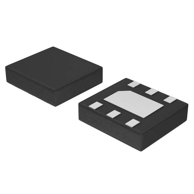
small DFNW6 2.2 x 2 mm, 0.65 pitch package.
Features
•
•
•
•
•
•
•
•
0.75 V – 5.5 V Operating Range
21 mW N MOSFET from 3.6 V to 5.5 V
22 mW N MOSFET from 1 V to 3.3 V
DC Current Up to 3 A
Output Auto−Discharge
Active High EN Pin
DFNW6 2.2 x 2 mm, 0.65 pitch
These Devices are Pb−Free, Halogen Free/BFR Free and are RoHS
Compliant
www.onsemi.com
MARKING
DIAGRAM
1
1
4A MG
G
DFNW6
CASE 507AF
4A
M
G
= Specific Device Code
= Date Code
= Pb−Free Package
(Note: Microdot may be in either location)
PINOUT DIAGRAM
GND
OUT
EN
EPAD
OUT
IN
IN
Typical Applications
• ADAS System
• Camera Module
• Power Management
© Semiconductor Components Industries, LLC, 2017
August, 2018 − Rev. 0
(Top View)
ORDERING INFORMATION
See detailed ordering, marking and shipping information on
page 8 of this data sheet.
1
Publication Order Number:
NCV451/D
�NCV451
Figure 1. Typical Application Circuit
PIN FUNCTION DESCRIPTION
Pin Name
Pin Number
Type
Description
IN
4, 5
POWER
Load−switch input voltage; connect a 1 mF or greater ceramic capacitor from IN to GND as
close as possible to the IC.
GND
1
POWER
Ground connection.
EN
6
INPUT
OUT
2, 3
OUTPUT
Load−switch output; connect a 1 mF ceramic capacitor from OUT to GND as close as
possible to the IC is recommended.
EPAD
7
POWER
Exposed pad, connect to ground potential.
Enable input, logic high turns on power switch.
BLOCK DIAGRAM
IN: Pin 4, 5
OUT: Pin 2, 3
Charge Pump and
soft start control
Control
logic
EN: Pin 6
EN Block
GND: Pin 1
Figure 2. Block Diagram
www.onsemi.com
2
�NCV451
MAXIMUM RATINGS
Symbol
Rating
Value
Unit
VEN, VIN, VOUT
−0.3 to + 7.0
V
From IN to OUT Pins: Input/Output (Note 1)
VIN, VOUT
0 to + 7.0
V
Human Body Model (HBM) ESD Rating are (Notes 1 and 2)
ESD HBM
1.5
kV
TJ
−40 to + 125
°C
Storage Temperature Range
TSTG
−40 to + 150
°C
Moisture Sensitivity (Note 3)
MSL
Level 1
IN, OUT, EN, Pins: (Note 1)
Maximum Junction Temperature
Stresses exceeding those listed in the Maximum Ratings table may damage the device. If any of these limits are exceeded, device functionality
should not be assumed, damage may occur and reliability may be affected.
1. According to JEDEC standard JESD22−A108.
2. This device series contains ESD protection and passes the following tests:
Human Body Model (HBM) ±1.5 kV per JEDEC standard: JESD22−A114 for all pins.
3. Moisture Sensitivity Level (MSL): 1 per IPC/JEDEC standard: J−STD−020.
OPERATING CONDITIONS
Symbol
Parameter
VIN
Operational Power Supply
VEN
Enable Voltage
Conditions
Max
Unit
0.75
Min
Typ
5.5
V
0
5.5
V
TA
Ambient Temperature Range
−40
25
+105
°C
TJ
Junction Temperature Range
−40
25
+125
°C
CIN
Decoupling input capacitor
COUT
Decoupling output capacitor
RqJA
Thermal Resistance Junction to Air
IOUT
Maximum DC current
PD
mF
1
mF
1
(Note 4)
°C/W
122
3
Power Dissipation Rating (Note 5)
0.164
A
W
Functional operation above the stresses listed in the Recommended Operating Ranges is not implied. Extended exposure to stresses beyond
the Recommended Operating Ranges limits may affect device reliability.
4. Value based on 1s0p board with copper 650 mm2 (or 1 in2) of 1 oz thickness and FR4 PCB substrate
5. The maximum power dissipation (PD) is given by the following formula:
PD +
www.onsemi.com
3
T JMAX * T A
R qJA
�NCV451
ELECTRICAL CHARACTERISTICS Min & Max Limits apply for TJ between −40°C to +125°C for VIN between 0.75 V to 5.0 V
(Unless otherwise noted). Typical values are referenced to TA = + 25 °C and VIN = 3.6 V (Unless otherwise noted).
Symbol
Parameter
Conditions
Min
Typ
Max
21
40
Unit
POWER SWITCH
IOUT = 200 mA, TA = 25°C
VIN = 5 V
TJ = 125°C
VIN = 3.6 V
Static drain−source on−state
resistance
Output discharge path
High−level input voltage
VIL
Low−level input voltage
IEN
EN pin leakage current
21
TJ = 125°C
40
50
IOUT = 200 mA, TA = 25°C
21
TJ = 125°C
mW
40
50
IOUT = 200 mA, TA = 25°C
23
TJ = 125°C
45
55
IOUT = 200 mA, TA = 25°C
VIN = 0.75 V
40
50
IOUT = 200 mA, TA = 25°C
VIN = 1.0 V
VIH
21
TJ = 125°C
VIN = 2.5 V
40
50
IOUT = 200 mA, TA = 25°C
VIN = 1.8 V
RDIS
21
TJ = 125°C
VIN = 3.3 V
RDS(on)
50
IOUT = 200 mA, TA = 25°C
25
TJ = 125°C
45
55
EN = low
1.0
1.7
kW
0.8
0.4
VIN = 3.6 V
V
0.1
mA
QUIESCENT CURRENT
Istd
Iq
Standby current
VIN = 4.2 V
EN = low, No load,
TA = −40°C to 85°C
0.9
3
mA
Quiescent current
VIN = 3.6 V
VIN = 2.5 V
VIN = 1.8 V
VIN = 1.2 V
VIN = 1.0 V
VIN = 0.75 V
EN = high, No load (Note 6)
8
15
mA
RL = 25 W, COUT = 1 mF
600
RL = 25 W, COUT = 1 mF
800
RL = 25 W, COUT = 1 mF
1400
RL = 25 W, COUT = 1 mF
55
RL = 10 W, COUT = 0.1 mF
540
RL = 10 W, COUT = 0.1 mF
670
RL = 10 W, COUT = 0.1 mF
1210
RL = 10 W, COUT = 0.1 mF
2.5
TIMINGS
TEN
Enable time
TR
Output rise time
TON
TF
ON time (TEN + TR)
VIN = 3.6 V
(Note 7)
Output fall time
ms
TIMINGS
TEN
Enable time
TR
Output rise time
TON
TF
ON time (TEN + TR)
VIN = 3.6 V
(Note 7)
Output fall time
ms
Product parametric performance is indicated in the Electrical Characteristics for the listed test conditions, unless otherwise noted. Product
performance may not be indicated by the Electrical Characteristics if operated under different conditions.
6. Production tested at VIN = 3.6 V.
7. Parameters are guaranteed for CLOAD and RLOAD connected to the OUT pin with respect to the ground
www.onsemi.com
4
�NCV451
TIMINGS
VIN
EN
VIH
VIL
VOUT
90% Vout
10% Vout
TEN TR
TF
TON
Figure 3. Enable, Rise and Fall Time
www.onsemi.com
5
�NCV451
ELECTRICAL CURVES
34
32
25
IOUT = 200 mA
RDS(on) (mW)
23
RDS(on) (mW)
IOUT = 200 mA
30
21
TJ = 25°C
19
28
125°C
26
24
85°C
22
25°C
20
18
−40°C
16
17
14
12
15
0
1
2
3
4
5
10
6
0
1
2
VIN (V)
22
85°C
1.2
1.0
18
0.8
25°C
0.6
−40°C
0.4
14
0.2
0
10
−60 −40 −20
0
20
40
60
80
100 120 140
0
1
2
3
4
5
JUNCTION TEMPERATURE (°C)
VIN (V)
Figure 6. RDS(on) vs. Temperature, Multi VIN
Voltage
Figure 7. Standby Current (mA) vs. VIN,
Multi Junction Temperature
20
6
MOSFET LEAKAGE CURRENT (nA)
600
−40°C
+25°C
+85°C
+125°C
18
16
14
IQ_IN (mA)
6
1.4
ISTD_IN (mA)
RDS(on) (mW)
26
5
Figure 5. RDS(on) vs. VIN, Low Load, Multi
Junction Temperature
VIN = 0.75 V
VIN = 1.0 V
VIN = 1.8 V
VIN = 2.5 V
VIN = 3.3 V
VIN = 3.6 V
VIN = 5.0 V
30
4
VIN (V)
Figure 4. RDS(on) vs. VIN, Low Load
34
3
12
10
8
6
4
2
500
85°C
400
300
200
25°C
100
−40°C
0
0
0
1
2
3
4
5
6
0
VIN (V)
1
2
3
4
5
VIN (V)
Figure 9. MOSFET Leakage Current (nA) vs. VIN,
Multi Junction Temperature
Figure 8. Quiescent Current (mA) vs. VIN,
Multi Junction Temperature
www.onsemi.com
6
6
�NCV451
ELECTRICAL CURVES
5
VEN = VIN = 5.5 V
VEN = VIN = 3.6 V
IENleak (nA)
4
3
2
1
0
−50
−25
0
25
50
75
100
JUNCTION TEMPERATURE (°C)
Figure 10. EN Pin Leakage vs. Junction
Temperature
www.onsemi.com
7
125
�NCV451
FUNCTIONAL DESCRIPTION
Overview
The auto−discharge is activated when EN pin is set to low
level (disable state).
The discharge path (Pull down NMOS) stays activated as
long as EN pin is set at low level and VIN > 0.75 V.
In order to limit the current across the internal discharge
N−MOSFET, the typical value is set at RDIS.
The NCV451 is a high side N channel MOSFET power
distribution switch designed to isolate ICs connected on the
battery in order to save energy. The part can be turned on,
with a wide range of battery from 0.75 V to 5.5 V.
Enable Input
Enable pin is an active high. The path is opened when EN
pin is tied low (disable), forcing N−MOSFET switch off.
The IN/OUT path is activated with a minimum of Vin of
0.75 V and EN forced to high level.
CIN and COUT Capacitors
IN and OUT, 1 mF, at least, capacitors must be placed as
close as possible the part to for stability improvement.
Auto Discharge
N−MOSFET is placed between the output pin and GND,
in order to discharge the application capacitor connected on
OUT pin.
APPLICATION INFORMATION
Power Dissipation
PCB Recommendations
Main contributor in term of junction temperature is the
power dissipation of the power MOSFET. Assuming this,
the power dissipation and the junction temperature in
normal mode can be calculated with the following
equations:
The NCV451 integrates an up to 3 A rated NMOS FET,
and the PCB design rules must be respected to properly
evacuate the heat out of the silicon. By increasing PCB area,
especially around IN and OUT pins, the RqJA of the package
can be decreased, allowing higher power dissipation.
Routing example: 2 oz, 4 layers with vias across 2 internal
inners.
P D + R DS(on)
ǒIOUTǓ
2
PD
= Power dissipation (W)
RDS(on)
IOUT
= Power MOSFET on resistance (W)
= Output current (A)
TJ + PD
R qJA ) T A
TJ
= Junction temperature (°C)
RqJA
TA
= Package thermal resistance (°C/W)
= Ambient temperature (°C)
ORDERING INFORMATION
Device
NCV451AMNWTBG
Marking
Option
Package
Shipping†
4A
Auto Discharge
1 kW
DFNW6
(Pb−Free)
3000 / Tape & Reel
†For information on tape and reel specifications, including part orientation and tape sizes, please refer to our Tape and Reel Packaging
Specifications Brochure, BRD8011/D.
www.onsemi.com
8
�MECHANICAL CASE OUTLINE
PACKAGE DIMENSIONS
DFNW6 2.0x2.2, 0.65P
CASE 507AF
ISSUE O
1
SCALE 2:1
PIN ONE
REFERENCE
L3
A
B
D
ÉÉÉ
ÉÉÉ
ÉÉÉ
DATE 18 AUG 2017
L
L
ALTERNATE
CONSTRUCTION
DETAIL A
E
EXPOSED
COPPER
DETAIL B
A1
A4
A
A3
PLATING
ALTERNATE
CONSTRUCTION
DETAIL B
C
0.05 C C
NOTE 4
A4
C
SIDE VIEW
SEATING
PLANE
PLATED
SURFACES
D2
DETAIL A
1
6X
DIM
A
A1
A3
A4
b
D
D2
E
E2
e
K
L
L3
A4
A1
TOP VIEW
0.05 C
NOTES:
1. DIMENSIONING AND TOLERANCING PER
ASME Y14.5M, 1994.
2. CONTROLLING DIMENSION: MILLIMETERS.
3. DIMENSION b APPLIES TO PLATED TERMINAL
AND IS MEASURED BETWEEN 0.15 AND
0.30mm FROM THE TERMINAL TIP.
4. COPLANARITY APPLIES TO THE EXPOSED
PAD AS WELL AS THE TERMINALS.
5. THIS DEVICE CONTAINS WETTABLE FLANK
DESIGN FEATURE TO AID IN FILLET FORMATION ON THE LEADS DURING MOUNTING.
L3
L3
SECTION C−C
3
MILLIMETERS
MIN
NOM
MAX
0.90
0.80
0.85
−−−
−−−
0.05
0.20 REF
0.10
−−−
−−−
0.20
0.25
0.30
1.90
2.00
2.10
1.50
1.60
1.70
2.10
2.20
2.30
0.79
0.89
0.99
0.65 BSC
0.26 REF
0.30
0.40
0.50
0.05 REF
GENERIC
MARKING DIAGRAM*
1
L
XX MG
G
E2
K
4
6
e
6X
b
XX
M
G
0.10 C A B
0.05 C
BOTTOM VIEW
NOTE 3
= Specific Device Code
= Date Code
= Pb−Free Package
(Note: Microdot may be in either location)
RECOMMENDED
SOLDERING FOOTPRINT*
1.70
*This information is generic. Please refer to
device data sheet for actual part marking.
Pb−Free indicator, “G” or microdot “ G”,
may or may not be present. Some products
may not follow the Generic Marking.
6X
0.56
0.99
2.50
1
0.65
PITCH
6X
0.27
PACKAGE
OUTLINE
DIMENSIONS: MILLIMETERS
*For additional information on our Pb−Free strategy and soldering
details, please download the ON Semiconductor Soldering and
Mounting Techniques Reference Manual, SOLDERRM/D.
DOCUMENT NUMBER:
DESCRIPTION:
98AON73486G
DFNW6 2.0X2.2, 0.65P
Electronic versions are uncontrolled except when accessed directly from the Document Repository.
Printed versions are uncontrolled except when stamped “CONTROLLED COPY” in red.
PAGE 1 OF 1
ON Semiconductor and
are trademarks of Semiconductor Components Industries, LLC dba ON Semiconductor or its subsidiaries in the United States and/or other countries.
ON Semiconductor reserves the right to make changes without further notice to any products herein. ON Semiconductor makes no warranty, representation or guarantee regarding
the suitability of its products for any particular purpose, nor does ON Semiconductor assume any liability arising out of the application or use of any product or circuit, and specifically
disclaims any and all liability, including without limitation special, consequential or incidental damages. ON Semiconductor does not convey any license under its patent rights nor the
rights of others.
© Semiconductor Components Industries, LLC, 2019
www.onsemi.com
�onsemi,
, and other names, marks, and brands are registered and/or common law trademarks of Semiconductor Components Industries, LLC dba “onsemi” or its affiliates
and/or subsidiaries in the United States and/or other countries. onsemi owns the rights to a number of patents, trademarks, copyrights, trade secrets, and other intellectual property.
A listing of onsemi’s product/patent coverage may be accessed at www.onsemi.com/site/pdf/Patent−Marking.pdf. onsemi reserves the right to make changes at any time to any
products or information herein, without notice. The information herein is provided “as−is” and onsemi makes no warranty, representation or guarantee regarding the accuracy of the
information, product features, availability, functionality, or suitability of its products for any particular purpose, nor does onsemi assume any liability arising out of the application or use
of any product or circuit, and specifically disclaims any and all liability, including without limitation special, consequential or incidental damages. Buyer is responsible for its products
and applications using onsemi products, including compliance with all laws, regulations and safety requirements or standards, regardless of any support or applications information
provided by onsemi. “Typical” parameters which may be provided in onsemi data sheets and/or specifications can and do vary in different applications and actual performance may
vary over time. All operating parameters, including “Typicals” must be validated for each customer application by customer’s technical experts. onsemi does not convey any license
under any of its intellectual property rights nor the rights of others. onsemi products are not designed, intended, or authorized for use as a critical component in life support systems
or any FDA Class 3 medical devices or medical devices with a same or similar classification in a foreign jurisdiction or any devices intended for implantation in the human body. Should
Buyer purchase or use onsemi products for any such unintended or unauthorized application, Buyer shall indemnify and hold onsemi and its officers, employees, subsidiaries, affiliates,
and distributors harmless against all claims, costs, damages, and expenses, and reasonable attorney fees arising out of, directly or indirectly, any claim of personal injury or death
associated with such unintended or unauthorized use, even if such claim alleges that onsemi was negligent regarding the design or manufacture of the part. onsemi is an Equal
Opportunity/Affirmative Action Employer. This literature is subject to all applicable copyright laws and is not for resale in any manner.
PUBLICATION ORDERING INFORMATION
LITERATURE FULFILLMENT:
Email Requests to: orderlit@onsemi.com
onsemi Website: www.onsemi.com
◊
TECHNICAL SUPPORT
North American Technical Support:
Voice Mail: 1 800−282−9855 Toll Free USA/Canada
Phone: 011 421 33 790 2910
Europe, Middle East and Africa Technical Support:
Phone: 00421 33 790 2910
For additional information, please contact your local Sales Representative
�