NCV7240, NCV7240A,
NCV7240B
Octal Low-Side
Relay Driver
The NCV7240 is an automotive eight channel low−side driver
providing drive capability up to 600 mA per channel. Output control is
via a SPI port and offers convenient reporting of faults for open load
(or short to ground), over load, and over temperature conditions.
Additionally, parallel control of the outputs is addressable (in pairs)
via the INx pins.
A dedicated limp−home mode pin (LHI) enables OUT1−OUT4
while disabling OUT5−OUT8.
Each output driver is protected for over load current and includes an
output clamp for inductive loads.
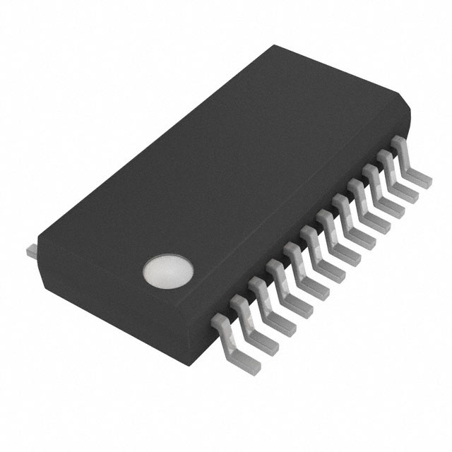
The NCV7240 is available in a SSOP−24 fused lead package.
www.onsemi.com
MARKING
DIAGRAM
NCV7240x
AWLYWWG
SSOP−24
CASE 565AL
Features
• 8 Channels
• 600 mA Low−Side Drivers
•
•
•
•
•
•
•
•
•
•
•
RDS(on) 1.5 W (Typ), 3 W (Max)
16−bit SPI Control
♦ Frame Error Detection (8−bit)
♦ Daisy Chain Capable
Parallel Input Pins for PWM operation
Power Up Without Open Circuit Detection Active (for LED
applications)
Low Quiescent Current in Sleep and Standby Modes
Limp Home Functionality
3.3 V and 5 V compatible Digital Input Supply Range
Fault Reporting
♦ Open Load Detection (selectable)
♦ Over Load
♦ Over Temperature
Power−on Reset (VDD, VDDA)
SSOP−24 Package (internally fused leads)
NCV Prefix for Automotive and Other Applications Requiring
Unique Site and Control Change Requirements; AEC−Q100
Qualified and PPAP Capable
These are Pb−Free Devices
♦
NCV7240x = Specific Device Code
(x = blank, A or B)
A
= Assembly Location
WL
= Wafer Lot
Y
= Year
WW
= Work Week
G
= Pb−Free Package
ORDERING INFORMATION
See detailed ordering and shipping information in the package
dimensions section on page 27 of this data sheet.
Applications
•
•
•
•
•
Automotive Body Control Unit
Automotive Engine Control Unit
Relay Drive
LED Drive
Stepper Motor Driver
© Semiconductor Components Industries, LLC, 2017
June, 2018 − Rev. 12
1
Publication Order Number:
NCV7240/D
�NCV7240, NCV7240A, NCV7240B
VDDA
VDD
Bias, Supply monitoring & POR
EN
OUT1
OUT1
OUT2
CSB
SCLK
SI
SO
OUT2
OUT3
OUT3
OUT4
OUT4
OUT5
OUT5
OUT6
OUT6
OUT7
OUT1−OUT4
ON
OUT7
SPI
OUT8
OUT8
GND
LHI
IN1
IN2
IN3
IN4
OUT1 & 5
OUT2 & 5
OUT3 & 7
OUT4 & 8
Figure 1. Basic Block Diagram
www.onsemi.com
2
�NCV7240, NCV7240A, NCV7240B
NCV7240
VDDA
VDD
0.1uF
OUT1
OUT2
3.3V 0.1uF
or
5V
OUT3
OUT4
microprocessor
OUT5
SO
OUT6
CSB
OUT7
SCLK
OUT8
SI
GND
EN
GND
GND
Limp Home
Control Circuit
5V
10uF
IN1
IN2
IN3
IN4
LHI
GND
Figure 2. Application Diagram (relay loads)
1
GND
VDDA
GND
CSB
OUT1
SI
OUT2
EN
OUT3
SCLK
OUT4
SO
OUT5
LHI
OUT6
IN1
OUT7
IN2
OUT8
IN3
GND
IN4
GND
VDD
Figure 3. Pinout
www.onsemi.com
3
Vbat
14V
�NCV7240, NCV7240A, NCV7240B
PACKAGE PIN DESCRIPTION
SSOP−24
Symbol
1
GND
Ground.
Description
2
GND
Ground.
3
OUT1
Channel 1 low−side drive output. Requires an external pull−up device for operation.
4
OUT2
Channel 2 low−side drive output. Requires an external pull−up device for operation.
5
OUT3
Channel 3 low−side drive output. Requires an external pull−up device for operation.
6
OUT4
Channel 4 low−side drive output. Requires an external pull−up device for operation.
7
OUT5
Channel 5 low−side drive output. Requires an external pull−up device for operation.
8
OUT6
Channel 6 low−side drive output. Requires an external pull−up device for operation.
9
OUT7
Channel 7 low−side drive output. Requires an external pull−up device for operation.
10
OUT8
Channel 8 low−side drive output. Requires an external pull−up device for operation.
11
GND
Ground.
12
GND
Ground.
13
VDD
Digital Power Supply for SO output (3.3 V or 5 V).
14
IN4
Parallel control of OUT4 and OUT8
Ground if not used for best EMI performance.
Alternatively keep open and internal pull−down will hold the input low.
(120 kW pull down resistor).
15
IN3
Parallel control of OUT3 and OUT7
Ground if not used for best EMI performance.
Alternatively keep open and internal pull−down will hold the input low.
(120 kW pull down resistor).
16
IN2
Parallel control of OUT2 and OUT6.
Ground if not used for best EMI performance.
Alternatively keep open and internal pull−down will hold the input low.
(120 kW pull down resistor).
17
IN1
Parallel control of OUT1 and OUT5.
Ground if not used for best EMI performance.
Alternatively keep open and internal pull−down will hold the input low.
(120 kW pull down resistor).
18
LHI
Limp Home Input. Active High.
A high on this pin powers up the device and activates the respective output drive INx designator while
disabling outputs OUT5−OUT8.
Input SPI commands are ignored, but the output register reports faults.
(Read capability only. No write capability.)
All registers are reset coming out of LHI mode.
Ground if not used for best EMI performance.
Alternatively keep open and internal pull−down resistor (120 kW) will hold the input low.
19
SO
SPI serial data output. Output high voltage level referenced to pin VDD.
20
SCLK
21
EN
Global Enable (active high). (120 kW pull down resistor).
22
SI
SPI serial data input (120 kW pull down resistor).
23
CSB
24
VDDA
SPI clock (120 kW pull down resistor).
SPI Chip Select ”Bar” (120 kW pull up resistor to VDD).
Analog Power Supply Input voltage (5 V).
www.onsemi.com
4
�NCV7240, NCV7240A, NCV7240B
MAXIMUM RATINGS
Min
Max
Supply Input Voltage (VDDA, VDD)
DC
Parameter
Unit
−0.3
5.5
Digital I/O pin voltage
(EN, LHI, Inx, CSB, SCLK, SI)
(SO)
−0.3
−0.3
5.5
VDD + 0.3
High Voltage Pins (OUTx)
DC
Peak Transient
−0.3
36
44 (Note 1)
Output Current (OUTx)
−1
1.3
Clamping Energy
Maximum (single pulse)
Repetitive (multiple pulse) (Note 2)
−
−
75
−
Operating Junction Temperature Range
−40
150
°C
Storage Temperature Range
−55
150
°C
ESD Capability,
Human body model (100 pF, 1.5 kW) (OUTx pins)
Human body model (100 pF, 1.5 kW) (all other pins)
−4000
−2000
4000
2000
ESD Capability
Machine Model (200 pF)
−200
200
Grade A
−
V
V
V
A
mJ
V
V
AECQ10x−12−RevA
Short Circuit Reliability Characterization
PACKAGE
Moisture Sensitivity Level
MSL2
Lead Temperature Soldering: SMD style only, Reflow (Note 3)
Pb−Free Part 60 − 150 sec above 217°C, 40 sec max at peak
−
265 peak
°C
°C/W
Package Thermal Resistance (per JESD51)
SSOP−24
Junction−to−Ambient (1s0p + 600 mm2 Cu) (Note 4)
Junction−to−Ambient (2s2p) (Notes 4 and 5)
Junction−to−Pin (pins 1, 2, 11, 12) (Note 6)
68
62
30
Stresses exceeding those listed in the Maximum Ratings table may damage the device. If any of these limits are exceeded, device functionality
should not be assumed, damage may occur and reliability may be affected.
1. Internally limited. Specification applies to unpowered and powered modes. (0 V to VDDA, 0 V to VDD)
2. Testing particulars, 2M pulses, Vbat = 15 V, 63 W, 390 mH, TA = 25°C. (See Figure 4)
3. For additional information, see or download ON Semiconductor’s Soldering and Mounting Techniques Reference Manual, SOLDERRM/D
and Application Note AND8083/D.
4. 76 mm x 76 mm x 1.5 mm FR4 PCB with additional heat spreading copper (2 oz) of 600 mm2, LS1 to LS8 dissipating 100 mW each. No
vias.
5. Include 2 inner 1 oz copper layers. No vias.
6. One output dissipating 100 mW.
Figure 4. Repetitive Clamping Energy Test
www.onsemi.com
5
�NCV7240, NCV7240A, NCV7240B
ELECTRICAL CHARACTERISTICS (3.0 V < VDD < VDDA, 4.5 V < VDDA (Note 7) < 5.5 V, −40°C v TJ v 150°C, EN = VDD,
LHI = 0 V unless otherwise specified).
Symbol
Characteristic
Conditions
Min
Typ
Max
−
3
5
Unit
GENERAL
IVDDA_ON
Operating Current (VDDA)
ON Mode
(All Channels On)
mA
SI = SCLK = 0 V, CSB = VDD
TJ = 25°C
TJ = 85°C
TJ = 150°C
−
−
−
Quiescent Current (VDDA)
Low Iq Mode
SI = SCLK = EN = 0 V, CSB = VDD
TJ = 25°C
TJ = 85°C
TJ = 150°C
−
−
−
−
−
−
10
10
20
Operating Current (VDD)
ON Mode
(All Channels On)
EN=high, SCLK = Inx = 0 V,
CSB = VDD = VDDA
−
0.3
0.5
CSB = VDD = VDDA, fSCLK = 0 Hz
TJ = 25°C
TJ = 85°C
TJ = 150°C
−
−
−
−
−
−
20
20
40
Quiescent Current (VDD)
Low Iq Mode
EN = 0 V
TJ = 25°C
TJ = 85°C
TJ = 150°C
−
−
−
−
−
−
5
5
20
POR_VDDA_rise
NCV7240 / NCV7240A
Power−on Reset threshold (VDDA)
VDDA rising
−
3.80
4.15
V
POR_VDDA_hys
NCV7240 / NCV7240A
Power−on Reset hysteresis (VDDA)
150
200
350
mV
POR_VDDA_rise
NCV7240B
Power−on Reset threshold (VDDA)
VDDA rising
−
3.60
3.85
V
POR_VDDA_fall
NCV7240B
Power−on Reset threshold (VDDA)
VDDA falling
3.00
3.30
3.50
V
POR_VDD_hys
NCV7240B
Power−on Reset hysteresis (VDDA)
150
200
350
mV
POR_VDDA_rise
Power−on Reset threshold (VDD)
IVDDA_GS_25
IVDDA_GS_85
IVDDA_GS_150
IVDDA_LO_25
IVDDA_LO_85
IVDDA_LO_150
IVDD_ON
IVDD_GS_25
IVDD_GS_85
IVDD_GS_150
IVDD_LO_25
IVDD_LO_85
IVDD_LO_150
POR_VDD_hys
TSD
TSDhys
Quiescent Current (VDDA)
Global Standby Mode
(All Channels Off)
mA
Quiescent Current (VDD)
Global Standby Mode
(All Channels Off)
VDD rising
Power−on Reset Hysteresis (VDD)
32
35
40
mA
mA
mA
mA
−
2.4
2.7
V
75
100
240
mV
Thermal Shutdown (Note 8)
Not ATE tested.
150
175
200
°C
Thermal Hysteresis
Not ATE tested.
10
25
−
°C
Output Transistor RDS(on)
IOUTx = 180 mA
−
1.5
3.0
W
0.6
0.95
1.3
A
OUTPUT DRIVER
RDS(on)
IOL
Ileak_typ
Overload Detection Current
Output Leakage
OUTx = 13.5 V, 25°C
OUTx = 13.5 V
OUTx = 35 V
−
−
−
−
−
−
1
5
10
mA
Output Clamp Voltage
VDD = 0 V to 5.5 V
VDDA = 0 V to 5.5 V
IOUTx = 50 mA
36
40
44
V
Ileak_temp
Ileak_HV
CLAMP
BODY
Output Body Diode Voltage
OPEN_V
Open Load Detection Threshold
Voltage (Vol)
OPEN_I
Open Load Diagnostic Sink Current (Iol)
IOUTx = −180mA
1 V < OUTx < 13.5 V, Output
Disabled
−
−
1.5
V
1.0
1.75
2.5
V
20
60
100
mA
7. Reduced performance down to 4 V provided VDDA Power−On Reset threshold has not been breached.
8. Each output driver is protected by its’ own individual thermal sensor.
9. Input signals H→L→H greater than 50usec are guaranteed to be detected.
www.onsemi.com
6
�NCV7240, NCV7240A, NCV7240B
ELECTRICAL CHARACTERISTICS (3.0 V < VDD < VDDA, 4.5 V < VDDA (Note 7) < 5.5 V, −40°C v TJ v 150°C, EN = VDD,
LHI = 0 V unless otherwise specified).
Symbol
Characteristic
Conditions
Min
Typ
Max
Unit
CSB = 0 V, EN going high 80% to SO
active
−
−
200
ms
50
−
−
ms
OUTPUT TIMING SPECIFICATIONS
tWU
Enable (EN) wake−up time
tSig
Enable (EN) and LHI (Note 9) Signal Duration
tSPI_ON
Serial Control
Output turn−on time
All Channels
CSB going high 80% to OUTx going
low 20% Vbat ,Vbat = 13.5 V,
IDS = 180 mA resistive load
−
30
50
ms
tSPI_OFF
Serial Control
Output turn−off time
All Channels
CSB going high 80% to OUTx going
high 80% Vbat, Vbat = 13.5 V,
IDS = 180 mA resistive load
−
30
50
ms
tLogic_ON
Parallel Control
Output turn−on time
All Channels
INx going high 80% to OUTx going
low 20% Vbat, Vbat = 13.5 V,
IDS = 180 mA resistive load
−
30
50
ms
tLogic_OFF
Parallel Control
Output turn−off time
All Channels
Inx going low 20% to OUTx going
high 80% Vbat, Vbat = 13.5 V,
IDS = 180 mA resistive load
−
30
50
ms
tOVER
Over Load Shut−Down Delay Time
3
15
50
ms
tOPEN
Open Load Detection Time
30
115
200
ms
Digital Input Threshold
(CSB, SI, SCLK, LHI, EN,INx)
0.8
1.4
2.0
V
LOGIC_H1
Digital Input Hysteresis
(CSB, SI, SCLK, INx)
50
175
300
mV
LOGIC_H2
Digital Input Hysteresis
(LHI, EN)
150
400
800
mV
Inx = SI = SCLK = LHI = EN = VDD
50
120
190
kW
CSB = 0 V
50
120
190
kW
DIGITAL INTERFACE CHARACTERISTICS
INPUT CHARACTERISTICS
LOGIC_V
RI_PD
Input Pulldown Resistance
(SI, SCLK, LHI, EN,INx)
RI_PU
Input Pullup Resistance (CSB)
CSB_leak_VDD
CSB_leak_VDDA
CSB Leakage to VDD
CSB Leakage to VDDA
CSB = 5 V, VDD = 0 V
−
−
100
uA
CSB = 5 V, VDDA = 0 V
−
−
100
uA
VDD −
0.4
−
−
V
OUTPUT CHARACTERISTICS
SO_HI
SO – Output High
I(out) = −1.5 mA
SO_LO
SO – Output Low
I(out) = 2.0 mA
−
−
0.6
V
CSB = VDD
−3
0
3
mA
SO_TS_leak
SO Tri−state Leakage
SPI TIMING (all timing specifications measured at 20% and 80% voltage levels)
freq
I/f
SCLK Frequency
−
−
5
MHz
200
−
−
ns
Figure 5, #1
85
−
−
ns
SCLK Clock Period
tSCLK_HI
SCLK High Time
tSCLK_LO
SCLK Low Time
Figure 5, #2
85
−
−
ns
tSI_SU
SI Setup Time
Figure 5, #11
50
−
−
ns
tSI_hold
SI Hold Time
Figure 5, #12
50
−
−
ns
tCSB_SU
CSB Setup Time
Figure 5, #5, 6
100
−
−
ns
tCSB_HI
CSB High Time
Figure 5, #7
1.5
−
−
ms
Figure 5, #3, 4
85
−
−
ns
Figure 5, #8, Cload = 50 pF
Not ATE tested
−
−
200
ns
tSCLK_SU
tSO_EN
SCLK Setup Time
SO Output Enable Time
(CSB falling to SO valid)
7. Reduced performance down to 4 V provided VDDA Power−On Reset threshold has not been breached.
8. Each output driver is protected by its’ own individual thermal sensor.
9. Input signals H→L→H greater than 50usec are guaranteed to be detected.
www.onsemi.com
7
�NCV7240, NCV7240A, NCV7240B
ELECTRICAL CHARACTERISTICS (3.0 V < VDD < VDDA, 4.5 V < VDDA (Note 7) < 5.5 V, −40°C v TJ v 150°C, EN = VDD,
LHI = 0 V unless otherwise specified).
Symbol
Characteristic
Conditions
Min
Typ
Max
Unit
Figure 5, #9
Not ATE tested
−
−
200
ns
Figure 5, #10, Cload = 50 pF
Not ATE tested
−
−
100
ns
SPI TIMING (all timing specifications measured at 20% and 80% voltage levels)
tSO_DIS
SO Output Disable Time
(CSB rising to SO tri−state)
tSO_valid
SO Output Data Valid Time with
capacitive load
7. Reduced performance down to 4 V provided VDDA Power−On Reset threshold has not been breached.
8. Each output driver is protected by its’ own individual thermal sensor.
9. Input signals H→L→H greater than 50usec are guaranteed to be detected.
Product parametric performance is indicated in the Electrical Characteristics for the listed test conditions, unless otherwise noted. Product
performance may not be indicated by the Electrical Characteristics if operated under different conditions.
www.onsemi.com
8
�NCV7240, NCV7240A, NCV7240B
4
7
CSB
6
5
SCLK
1
2
3
CSB
SO
8
9
SI
12
SCLK
10
11
SO
Figure 5. Detailed SPI Timing (measured at 20% and 80% voltage levels)
www.onsemi.com
9
�NCV7240, NCV7240A, NCV7240B
TYPICAL PERFORMANCE GRAPHS
6.0
VDDA LOW Iq CURRENT (mA)
0.7
0.6
0.5
0.4
0.3
0.2
0.1
3.0
−40°C
2.0
25°C
1.0
0
20
40
60
80
100
120
140
3
3.5
4
4.5
5
5.5
TEMPERATURE (°C)
VDDA (V)
Figure 6. VDD Low Iq Current vs. Temperature
Figure 7. VDDA Low Iq Quiescent Current vs.
VDDA
4.5
1.4
4
1.2
3.5
3
2.5
2
1.5
1
VDDA = 5 V
0.5
0
−40
1.0
0.8
0.6
150°C
0.4
25°C
0.2
−40°C
−20
0
20
40
60
80
100
120
0
140
3
3.5
4
4.5
5
5.5
TEMPERATURE (°C)
VDD (V)
Figure 8. VDDA Low Iq Current vs.
Temperature
Figure 9. VDD Low Iq Current vs. VDD
44
44
43
43
42
42
41
40
39
38
37
36
50
150°C
4.0
0
−20
VDD LOW Iq CURRENT (mA)
VDDA LOW Iq CURRENT (mA)
0
−40
OUTPUT VOLTAGE (V)
5.0
VDD = 5 V
CLAMP VOLTAGE (V)
VDD LOW Iq CURRENT (mA)
0.8
180 mA
41
40
50 mA
39
38
37
70
90
110
130
150
36
−40 −20
170
0
20
40
60
80
100
120 140
OUTPUT CURRENT (mA)
TEMPERATURE (°C)
Figure 10. Output Clamp Voltage vs. Current
Figure 11. Output Clamp Voltage vs.
Temperature
www.onsemi.com
10
�NCV7240, NCV7240A, NCV7240B
TYPICAL PERFORMANCE GRAPHS
1.3
3.0
DETECTION CURRENT (A)
2.5
IOUT = 600 mA
RDS(on) (W)
2.0
IOUT = 100 mA
1.5
1.0
0.5
0
−40 −20
0
20
40
60
80
100
120
1.1
1.0
0.9
0.8
0.7
0.6
−40
140
−20
0
40
60
80
100
120
140
TEMPERATURE (°C)
Figure 12. Output RDS(on) vs. Temperature
Figure 13. Over Load Current vs. Temperature
1.0
T = 150°C
0.9
LEAKAGE CURRENT (mA)
0.9
0.8
0.7
0.6
0.5
0.4
0.3
0.2
0.1
OUTx = 13.5 V
0.8
0.7
0.6
0.5
0.4
0.3
0.2
0.1
0
13.5
14
14.5
15
15.5
16
16.5
17
17.5
0
−40
18
−20
0
OUTPUT VOLTAGE (V)
20
40
60
80
100
120
140
TEMPERATURE (°C)
Figure 14. Output Leakage vs. Voltage (1505C)
OPEN LOAD DETECTION CURRENT (mA)
20
TEMPERATURE (°C)
1.0
OUTPUT CURRENT (mA)
1.2
Figure 15. Output Leakage vs. Temperature
2.5
100
90
THRESHOLD VOLTAGE
80
70
60
50
40
30
20
10
0
−40
2.0
1.5
1.0
0.5
OUTx = 13.5 V
−20
0
20
40
60
80
100
120
0
−40
140
−20
0
20
40
60
80
100
120
140
TEMPERATURE (°C)
TEMPERATURE (°C)
Figure 16. Output Load Detection Current vs.
Temperature
Figure 17. Open Load Detection Voltage vs.
Temperature
www.onsemi.com
11
�NCV7240, NCV7240A, NCV7240B
TYPICAL PERFORMANCE GRAPHS
1.0
BODY DIODE VOLTAGE
0.9
0.8
0.7
0.6
0.5
0.4
0.3
0.2
0.1
0
−40
IOUT = −180 mA
−20
0
20
40
60
80
100
120
140
TEMPERATURE (°C)
Figure 18. Output Body Diode Voltage vs.
Temperature
www.onsemi.com
12
�NCV7240, NCV7240A, NCV7240B
DETAILED OPERATING DESCRIPTION
Power Outputs
EN pin. The NCV7240 device will go through a power up
reset each time the EN pin is toggled high resulting in a
device setup of default values as described in the Register
Specifics section. Standby Mode, Input Mode, ON Mode,
and OFF Mode are all selectable via the SPI for each channel
independently.
The NCV7240 provides eight independent 600mA power
transistors with their source connection referenced to the
ground pin and with their drain connection brought out to
individual pins resulting in 8 independent low−side drivers.
Output driver location on one side of the IC layout provides
for optimum pcb layout to the loads.
Internal clamping structures are provided to limit
transient voltages when switching inductive loads. Each
output has an over load detection current of 0.6 A (min)
where the drivers turn−off and stay latched off. An Over
Load Current Shut−Down Delay Time of 3 ms (min) is
designed into the IC as a filter allowing for spikes in current
which may occur during normal operation and allowing for
protection from overload conditions.
Faults can be cleared with the SPI input register
(command 00) or via a power−on−reset. Fault detection is
provided in real time. Detection is provided both during
output turn−on and with output already on. (See Page 18,
Clearing the Fault Registers)
The NCV7240 is available in a SSOP−24 package.
Power up, Power−On Reset (UVLO mode)
Both VDD and VDDA supply an independent
power−on−reset function to the IC. Coming out of
power−on−reset all input bits are set to a 1 (OFF Mode) and
all output bits are set to a 0 except for the TER bit which is
set to a 1. The device cannot operate without both supplies
above their respective power−on reset thresholds with the
exception of LHI mode. During LHI mode, VDD POR is
ignored and the device is only affected by VDDA POR.
The NCV7240 powers up into the Global OFF Mode
without the open circuit diagnostic current enabled. This
allows the device to be turned on via EN = 0 to EN = 1 with
LED loads avoiding illumination of the LED loads
(reference Figure 21 State Diagram). All other paths to
Global OFF Mode enable open circuit diagnostic current.
Output Control (SPI)
Each output driver is controlled via a digital SPI port after
the device has powered up (out of POR) and enabled via the
Table 1. MODES OF OPERATION
Modes of
Operation
Conditions
Description
UVLO Mode
VDD or VDDA below their respective POR
thresholds
All outputs off in this mode.
Coming out of this mode
with EN = 1 sets all channels in the OFF mode
without open circuit diagnostic current enabled.
With LHI = 1 and EN = x, the part enters limp home mode.
OFF Mode
SPI Control
(Command 11)
Output off.
Open circuit diagnostic current is disabled (powerup mode).
Open circuit diagnostic current is enabled (normal mode).
Global OFF Mode
SPI Control
All Channels (Command 11)
Output off.
Open circuit diagnostic current is disabled (powerup mode).
Open circuit diagnostic current is enabled (normal mode).
ON Mode
SPI Control
(Command 10)
Limp Home Mode
(LHI)
LHI = high, EN = x
Low Iq Mode
EN = LHI = low
Provides a state with the lowest quiescent current for VDD
and VDDA.
Standby Mode
SPI Control
(Command 00)
Provides an OFF state with
Open circuit diagnostic current disabled.
Global
Standby Mode
SPI Control
All Channels (Command 00)
Input Mode
SPI Control
(Command 01)
Output on.
Dedicated output turn on control of
OUT1−OUT4 using IN1−IN4.
OUT5−OUT8 are in OFF Mode.
Provides a reduced quiescent current mode.
Provides an OFF state with
Open circuit diagnostic current disabled.
Directs output channel to be driven from INx input pins.
www.onsemi.com
13
�NCV7240, NCV7240A, NCV7240B
Figure 19. Basic State Diagram
Figure 20. Normal Operation State Diagram
www.onsemi.com
14
�15
to
LHI Mode
www.onsemi.com
Figure 21. Detailed State Diagram
SPI code
= “0000h"
SO reports above VDD > POR
--- dotted line indicates bidirectional path.
SPI
CODE
SPI CODE
INPUT MODE
INPUT DATA“01”
INPUT PINS
MUXED TO
OUTPUTS
SPI CODE
LHI = EN = “0"
LHI = “1"
LHI = EN = “0"
SPI CODE
LOW_IQ Mode
(VDDA < POR) or
(VDD


 工商网监
湘ICP备2023018690号
工商网监
湘ICP备2023018690号
