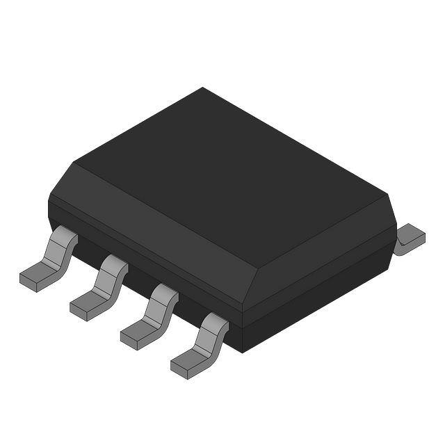
NCV7340
CAN Transceiver, High
Speed, Low Power
Description
The NCV7340 CAN transceiver is the interface between a
controller area network (CAN) protocol controller and the physical
bus and may be used in both 12 V and 24 V systems. The transceiver
provides differential transmit capability to the bus and differential
receive capability to the CAN controller.
The NCV7340 is a new addition to the CAN high−speed transceiver
family and is an improved drop−in replacement for the AMIS−42665.
Due to the wide common−mode voltage range of the receiver inputs,
the NCV7340 is able to reach outstanding levels of electromagnetic
susceptibility (EMS). Similarly, extremely low electromagnetic
emission (EME) is achieved by the excellent matching of the output
signals.
Features
• Compatible with the ISO 11898 Standard (ISO 11898−2, ISO
11898−5 and SAE J2284)
• Low Quiescent Current
• High Speed (up to 1 Mbps)
• Ideally Suited for 12 V and 24 V Industrial and Automotive
•
•
•
•
•
•
•
•
MARKING
DIAGRAM
8
8
NV7340−x
FALYW G
G
1
SOIC−8
CASE 751AZ
1
NV7340− = Specific Device Code
x = 3 (NCV7340D13R2G)
= 2 (NCV7340D12R2G)
= 4 (NCV7340D14R2G)
F
= Fab Location Code*
*For NCV7340D14R2G only
A
= Assembly Location
L
= Wafer Lot
Y
= Year
W
= Work Week
G
= Pb−Free Package
PIN ASSIGNMENT
1
8
2
7
TxD
STB
GND
3
VCC
NCV7340
•
•
•
•
Applications
Extremely Low Current Standby Mode with Wakeup via the Bus
Low EME Common−Mode Choke is No Longer Required
Voltage Source via VSPLIT Pin for Stabilizing the Recessive Bus
Level (Further EMC Improvement)
No Disturbance of the Bus Lines with an Un−powered Node
Transmit Data (TxD) Dominant Time−out Function
Thermal Protection
Bus Pins Protected Against Transients in an Automotive
Environment
Bus and VSPLIT Pins Short−Circuit Proof to Supply Voltage and
Ground
Logic Level Inputs Compatible with 3.3 V Devices
Up to 110 Nodes can be Connected to the Same Bus in Function of
Topology
NCV Prefix for Automotive and Other Applications Requiring
Unique Site and Control Change Requirements; AEC−Q100
Qualified and PPAP Capable
These are Pb−Free Devices
http://onsemi.com
CANH
6
CANL
5
4
VSPLIT
RxD
NCV7340DxxR2G
(Top View)
ORDERING INFORMATION
See detailed ordering and shipping information in the package
dimensions section on page 9 of this data sheet.
Typical Applications
• Automotive
• Industrial Networks
© Semiconductor Components Industries, LLC, 2014
October, 2014 − Rev. 8
1
Publication Order Number:
NCV7340/D
�NCV7340
Table 1. KEY TECHNICAL CHARACTERISTICS AND OPERATING RANGES
Min
Max
Unit
VCC
Symbol
Power supply voltage
Parameter
Conditions
4.75
5.25
V
VSTB
DC voltage at pin STB
0
VCC
V
VTxD
DC voltage at pin TxD
0
VCC
V
VRxD
DC voltage at pin RxD
0
VCC
V
VCANH
DC voltage at pin CANH
0 < VCC < 5.25 V; no time limit
−50
+50
V
VCANL
DC voltage at pin CANL
0 < VCC < 5.25 V; no time limit
−50
+50
V
VSPLIT
DC voltage at pin VSPLIT
0 < VCC < 5.25 V; no time limit
−40
+40
V
VO(dif)(bus_dom)
Differential bus output voltage in
dominant state
42.5 W < RLT < 60 W
1.5
3
V
CM−range
Input common−mode range for
comparator
Guaranteed differential receiver threshold
and leakage current
−35
+35
V
Cload
Load capacitance on IC outputs
15
pF
tpd(rec−dom)
Propagation delay TxD to RxD
See Figure 7
60
230
ns
tpd(dom−rec)
Propagation delay TxD to RxD
See Figure 7
60
245
ns
TJ
Junction temperature
−40
150
°C
BLOCK DIAGRAM
VCC
3
VCC
TxD
NCV7340
1
Timer
VCC
STB
RxD
GND
8
4
Thermal
shutdown
COMP
2
COMP
Figure 1. Block Diagram
http://onsemi.com
2
5
VSPLIT
6
Driver
control
Wakeup
Filter
CANH
VCC
VSPLIT
Mode &
wakeup
control
7
CANL
�NCV7340
TYPICAL APPLICATION
Application Schematics
VBAT
IN
5V−reg
OUT
VCC
VCC
3
STB
RxD
4
TxD
CANH
NCV7340
CAN
controller
RLT = 60 W
7
8
5
6
1
VSPLIT
CANL
2
GND
CLT = 47 nF
RLT = 60 W
GND
Figure 2. Application Diagram
Pin Description
1
GND
2
VCC
3
RxD
4
NCV7340
TxD
8
STB
7
CANH
6
CANL
5
VSPLIT
Figure 3. NCV7340 Pin Assignment
Table 2. PIN FUNCTION DESCRIPTION
Pin
Name
Description
1
TxD
Transmit data input; low input → dominant driver; internal pullup current
2
GND
Ground
3
VCC
Supply voltage
4
RxD
Receive data output; dominant transmitter → low output
5
VSPLIT
Common−mode stabilization output
6
CANL
Low−level CAN bus line (low in dominant mode)
7
CANH
High−level CAN bus line (high in dominant mode)
8
STB
Standby mode control input
http://onsemi.com
3
CAN
BUS
�NCV7340
FUNCTIONAL DESCRIPTION
Operating Modes
NCV7340 provides two modes of operation as illustrated
in Table 3. These modes are selectable through pin STB.
Split Circuit
The VSPLIT pin is operational only in normal mode. In
standby mode this pin is floating. The VSPLIT can be
connected as shown in Figure 2 or, if it’s not used, can be left
floating. Its purpose is to provide a stabilized DC voltage of
0.5 x VCC to the bus avoiding possible steps in the
common−mode signal therefore reducing EME. These
unwanted steps could be caused by an un−powered node on
the network with excessive leakage current from the bus that
shifts the recessive voltage from its nominal 0.5 x VCC
voltage.
Table 3. OPERATING MODES
Pin RXD
Pin
STB
Mode
Low
Normal
Bus dominant
Bus recessive
High
Standby
Wakeup request
detected
No wakeup
request detected
Low
High
Wakeup
When a valid wakeup (dominant state longer than tWake)
is received during the standby mode the RxD pin is driven
low. The wakeup detection is not latched: RxD returns to
High state after twakedr when the bus signal is released back
to recessive – see Figure 4. Wake−up behavior in case of a
permanent dominant − due to, for example, a bus short −
represents the only difference between the circuit functional
sub−versions listed in the Ordering Information table. When
the standby mode is entered while a dominant is present on
the bus, the “unconditioned bus wake−up” versions will
signal a bus−wakeup immediately after the state transition
(signal RxD1 in Figure 4). The other version will signal
bus−wakeup only after the initial dominant is released
(signal RxD2 in Figure 4). In this way it’s ensured, that a
CAN bus can be put to a low−power mode even if the nodes
have a level sensitivity to RxD pin and a permanent
dominant is present on the bus.
Normal Mode
In the normal mode, the transceiver is able to
communicate via the bus lines. The signals are transmitted
and received to the CAN controller via the pins TxD and
RxD. The slopes on the bus lines outputs are optimized to
give extremely low EME.
Standby Mode
In standby mode both the transmitter and receiver are
disabled and a very low−power differential receiver
monitors the bus lines for CAN bus activity. The bus lines
are terminated to ground and supply current is reduced to a
minimum, typically 10 mA. When a wake−up request is
detected by the low−power differential receiver, the signal
is first filtered and then verified as a valid wake signal after
a time period of tdwakerd, the RxD pin is driven low by the
transceiver to inform the controller of the wake−up request.
>tWake
1.4 V
0.75
2.5
5.0
ms
Vdif(dom) > 1.2 V
0.75
3
5.8
ms
tdwakerd
Delay to flag wake event (recessive to
dominant transitions) (See Figure 4)
Valid bus wake up event,
CRxD = 15 pF
1.0
3.4
10
ms
tdwakedr
Delay to flag end of wake event (dominant
to recessive transition) (See Figure 4)
Valid bus wake up event,
CRxD = 15 pF
0.5
2.9
6.0
ms
tWake(RxD)
Minimum pulse width on RxD (See Figure 4)
5 ms twake, CRxD = 15 pF
0.5
tdom(TxD)
TxD dominant time for time out
VTxD = 0 V
300
650
1000
http://onsemi.com
7
ms
ms
�NCV7340
MEASUREMENT SETUPS AND DEFINITIONS
+5 V
100 nF
VCC
3
NCV7340
1
RxD
CANH
7
TxD
4
1 nF
5
V SPLIT
Transient
Generator
1 nF
6
CANL
2
8
15 pF
GND
STB
Figure 5. Test Circuit for Automotive Transients
VRxD
High
Low
Hysteresis
0.9
0.5
Vi(dif)(hys)
Figure 6. Hysteresis of the Receiver
+5 V
100 nF
VCC
3
7
TxD
RxD
NCV7340
1
4
RLT
VSPLIT
60 W
6
CLT
100 pF
CANL
2
8
15 pF
5
CANH
STB
GND
Figure 7. Test Circuit for Timing Characteristics
http://onsemi.com
8
�NCV7340
HIGH
LOW
TxD
CANH
CANL
dominant
Vi(dif) =
VCANH − VCANL
0.9V
0.5V
recessive
RxD
0.7 x VCC
0.3 x VCC
td(TxD−BUSon)
td(TxD−BUSoff)
td(BUSon−RxD)
tpd(rec−dom)
tpd(dom−rec)
td(BUSoff−RxD)
Figure 8. Timing Diagram for AC Characteristics
DEVICE ORDERING INFORMATION
Part Number
NCV7340D12G
NCV7340D12R2G
NCV7340D13G
NCV7340D13R2G
NCV7340D14G
NCV7340D14R2G
Description
Temperature
Range
Package Type
96 Tube / Tray
HS LP CAN Transceiver
(Unconditioned Bus Wakeup)
EMC Improved
HS LP CAN Transceiver
(Unconditioned Bus Wakeup)
Shipping†
3000 / Tape & Reel
−40°C to +125°C
SOIC 150 8 (Mate Sn, JEDEC
MS−012)
(Pb−Free)
96 Tube / Tray
3000 / Tape & Reel
96 Tube / Tray
HS LP CAN Transceiver
(Bus Wakeup Inactive in
Case of Bus Fault)
3000 / Tape & Reel
†For information on tape and reel specifications, including part orientation and tape sizes, please refer to our Tape and Reel Packaging
Specifications Brochure, BRD8011/D.
http://onsemi.com
9
�MECHANICAL CASE OUTLINE
PACKAGE DIMENSIONS
SOIC−8
CASE 751AZ
ISSUE B
8
1
SCALE 1:1
NOTES 4&5
0.10 C D
45 5 CHAMFER
D
h
NOTE 6
D
A
8
DATE 18 MAY 2015
H
2X
5
0.10 C D
E
E1
NOTES 4&5
L2
1
0.20 C D
4
8X
B
NOTE 6
TOP VIEW
b
0.25
M
L
C
DETAIL A
C A-B D
NOTES 3&7
NOTE 7
c
0.10 C
e
A1
C
SIDE VIEW
NOTE 8
DIM
A
A1
A2
b
c
D
E
E1
e
h
L
L2
DETAIL A
A2
A
SEATING
PLANE
NOTES:
1. DIMENSIONING AND TOLERANCING PER ASME Y14.5M, 1994.
2. CONTROLLING DIMENSION: MILLIMETERS.
3. DIMENSION b DOES NOT INCLUDE DAMBAR PROTRUSION.
ALLOWABLE PROTRUSION SHALL BE 0.004 mm IN EXCESS OF
MAXIMUM MATERIAL CONDITION.
4. DIMENSION D DOES NOT INCLUDE MOLD FLASH, PROTRUSIONS
OR GATE BURRS. MOLD FLASH, PROTRUSIONS OR GATE BURRS
SHALL NOT EXCEED 0.006 mm PER SIDE. DIMENSION E1 DOES
NOT INCLUDE INTERLEAD FLASH OR PROTRUSION. INTERLEAD
FLASH OR PROTRUSION SHALL NOT EXCEED 0.010 mm PER SIDE.
5. THE PACKAGE TOP MAY BE SMALLER THAN THE PACKAGE BOT
TOM. DIMENSIONS D AND E1 ARE DETERMINED AT THE OUTER
MOST EXTREMES OF THE PLASTIC BODY AT DATUM H.
6. DIMENSIONS A AND B ARE TO BE DETERMINED AT DATUM H.
7. DIMENSIONS b AND c APPLY TO THE FLAT SECTION OF THE LEAD
BETWEEN 0.10 TO 0.25 FROM THE LEAD TIP.
8. A1 IS DEFINED AS THE VERTICAL DISTANCE FROM THE SEATING
PLANE TO THE LOWEST POINT ON THE PACKAGE BODY.
SEATING
PLANE
END VIEW
RECOMMENDED
SOLDERING FOOTPRINT*
MILLIMETERS
MIN
MAX
--1.75
0.10
0.25
1.25
--0.31
0.51
0.10
0.25
4.90 BSC
6.00 BSC
3.90 BSC
1.27 BSC
0.25
0.41
0.40
1.27
0.25 BSC
GENERIC
MARKING DIAGRAM*
8X
0.76
8
8X
1.52
1
7.00
XXXXX
A
L
Y
W
G
1
1.27
PITCH
DIMENSIONS: MILLIMETERS
*For additional information on our Pb−Free strategy and soldering
details, please download the ON Semiconductor Soldering and
Mounting Techniques Reference Manual, SOLDERRM/D.
DOCUMENT NUMBER:
DESCRIPTION:
98AON34918E
SOIC−8
XXXXX
ALYWX
G
= Specific Device Code
= Assembly Location
= Wafer Lot
= Year
= Work Week
= Pb−Free Package
*This information is generic. Please refer
to device data sheet for actual part
marking. Pb−Free indicator, “G”, may
or not be present.
Electronic versions are uncontrolled except when accessed directly from the Document Repository.
Printed versions are uncontrolled except when stamped “CONTROLLED COPY” in red.
PAGE 1 OF 1
ON Semiconductor and
are trademarks of Semiconductor Components Industries, LLC dba ON Semiconductor or its subsidiaries in the United States and/or other countries.
ON Semiconductor reserves the right to make changes without further notice to any products herein. ON Semiconductor makes no warranty, representation or guarantee regarding
the suitability of its products for any particular purpose, nor does ON Semiconductor assume any liability arising out of the application or use of any product or circuit, and specifically
disclaims any and all liability, including without limitation special, consequential or incidental damages. ON Semiconductor does not convey any license under its patent rights nor the
rights of others.
© Semiconductor Components Industries, LLC, 2019
www.onsemi.com
�onsemi,
, and other names, marks, and brands are registered and/or common law trademarks of Semiconductor Components Industries, LLC dba “onsemi” or its affiliates
and/or subsidiaries in the United States and/or other countries. onsemi owns the rights to a number of patents, trademarks, copyrights, trade secrets, and other intellectual property.
A listing of onsemi’s product/patent coverage may be accessed at www.onsemi.com/site/pdf/Patent−Marking.pdf. onsemi reserves the right to make changes at any time to any
products or information herein, without notice. The information herein is provided “as−is” and onsemi makes no warranty, representation or guarantee regarding the accuracy of the
information, product features, availability, functionality, or suitability of its products for any particular purpose, nor does onsemi assume any liability arising out of the application or use
of any product or circuit, and specifically disclaims any and all liability, including without limitation special, consequential or incidental damages. Buyer is responsible for its products
and applications using onsemi products, including compliance with all laws, regulations and safety requirements or standards, regardless of any support or applications information
provided by onsemi. “Typical” parameters which may be provided in onsemi data sheets and/or specifications can and do vary in different applications and actual performance may
vary over time. All operating parameters, including “Typicals” must be validated for each customer application by customer’s technical experts. onsemi does not convey any license
under any of its intellectual property rights nor the rights of others. onsemi products are not designed, intended, or authorized for use as a critical component in life support systems
or any FDA Class 3 medical devices or medical devices with a same or similar classification in a foreign jurisdiction or any devices intended for implantation in the human body. Should
Buyer purchase or use onsemi products for any such unintended or unauthorized application, Buyer shall indemnify and hold onsemi and its officers, employees, subsidiaries, affiliates,
and distributors harmless against all claims, costs, damages, and expenses, and reasonable attorney fees arising out of, directly or indirectly, any claim of personal injury or death
associated with such unintended or unauthorized use, even if such claim alleges that onsemi was negligent regarding the design or manufacture of the part. onsemi is an Equal
Opportunity/Affirmative Action Employer. This literature is subject to all applicable copyright laws and is not for resale in any manner.
PUBLICATION ORDERING INFORMATION
LITERATURE FULFILLMENT:
Email Requests to: orderlit@onsemi.com
onsemi Website: www.onsemi.com
◊
TECHNICAL SUPPORT
North American Technical Support:
Voice Mail: 1 800−282−9855 Toll Free USA/Canada
Phone: 011 421 33 790 2910
Europe, Middle East and Africa Technical Support:
Phone: 00421 33 790 2910
For additional information, please contact your local Sales Representative
�