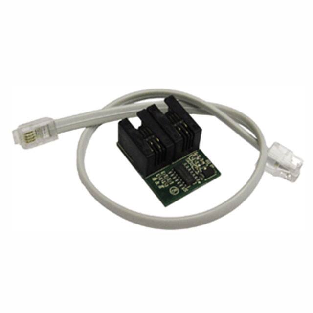
NCV7430 LIN RGB LED
Driver Evaluation Board
User's Manual
NCV74300V2GEVB
Introduction
www.onsemi.com
EVAL BOARD USER’S MANUAL
14
1
SOIC−14
D2 SUFFIX
CASE 751A
PIN ASSIGNMENT
ANODE
Features
• Small Size of PCB
• Two Parallelized Connectors for Easy Daisy-chain Connection
VBIAS
VBB
Applications
• Automotive Interior Lighting
LIN
Board Hardware
GND
TST2
GND
1
14
2
13
3
12
NCV7430
The NCV74300V2GEVB is an evaluation board for single-chip
RGB driver NCV7430, intended for dedicated multicolor LED
applications. The RGB LED driver contains a LIN interface (slave) for
parametric programming of LED color and intensity.
The device receives instructions through the LIN bus and
subsequently drives the LEDs independently.
The NCV7430 acts as a slave on the LIN bus and the master can
request specific status information (parameter values and error flags).
The LIN address of the NCV7430 can be programmed in the internal
memory of the device.
The design incorporates the lowest bill of materials, minimized
board size and allows easy interconnection in case of multiple nodes
network.
4
5
11
10
6
9
7
8
LED3C
LED1C
LED2C
TST1
LED2R
LED1R
LED3R
MARKING DIAGRAM
14
NCV7430−0
AWLYWWG
1
NCV7430
A
WL
Y
WW
G
© Semiconductor Components Industries, LLC, 2013
August, 2020 − Rev. 1
1
= Specific Device Code
= Assembly Location
= Wafer Lot
= Year
= Work Week
= Pb−Free Package
Publication Order Number:
EVBUM2208/D
�NCV74300V2GEVB
ABSOLUTE MAXIMUM RATINGS AND OPERATING RANGES
Table 1. ABSOLUTE MAXIMUM RATINGS
(The operation of the NCV7430 evaluation board works with the custom made ON Semiconductor LIN Interface in combination with the
custom GUI interface. No additional power supply is needed other than the supplied 12 V AC/DC adapter which powers the LIN Interface
through DC Power Input connector.)
Symbol
Parameter
Min
Max
Unit
LIN INTERFACE
VBUS
USB Supply Voltage
−0.3
5.5
V
VBAT
External Supply Voltage
−0.3
42
V
IBAT
Maximum Supply Current
−
2
A
VLIN
Maximum Voltage at LIN Bus Pin
−45
45
V
Ambient Temperature
−40
85
°C
VBAT
Supply Voltage
−0.3
43
V
VLIN
Maximum Voltage at LIN Bus Pin
−45
45
V
TJ
NCV7430 Junction Temperature
−40
150
°C
TA
Ambient Temperature
−40
125
°C
TA
NCV7430 EVB
Stresses exceeding those listed in the Maximum Ratings table may damage the device. If any of these limits are exceeded, device functionality
should not be assumed, damage may occur and reliability may be affected.
Table 2. RECOMMENDED OPERATING RANGES
Symbol
Parameter
Min
Max
Unit
LIN INTERFACE
VBUS
USB Supply Voltage
4.75
5.25
V
VBAT
External Supply Voltage
5.5
18
V
VLIN
Operating Voltage at LIN Bus Pin
5.5
18
V
Ambient Temperature
−40
85
°C
VBAT
Supply Voltage
5.5
18
V
VLIN
Operating Voltage at LIN Bus Pin
5.5
18
V
TJ
NCV7430 Junction Temperature
−40
125
°C
TA
Ambient Temperature
−40
105
°C
TA
NCV7430 EVB
www.onsemi.com
2
�NCV74300V2GEVB
Table 3. PIN FUNCTION DESCRIPTION
Connector
Pin
Pin Name
1
VBAT
Description
LIN INTERFACE
VBAT External Power Supply Input (LIN Interface + NCV7430 EVB Supply)
Power
LIN (RJ11)
2
LIN
3
GND
4
NC
USB
VBAT Supply Voltage Output/Input (LIN Interface can be supplied through this pin)
LIN Bus Line
Ground Connection
Not Connected
USB Connector
NCV7430 EVB
RJ11 (J1, J2)
(Note 1)
1
VBAT
2
LIN
3
GND
4
NC
Battery Supply Input/Output (Note 2)
LIN Bus Line
Ground Connection
Not Connected
1. Both connectors pinout is identical.
2. Connectors J1 and J2 are connected in parallel. Typically, J1 is a supply input while J2 is a supply output, which supplies the next board in
the serial chain.
Figure 1. NCV7430 EVB Pins Connections
Figure 2. LIN Cable with RJ11 4P4C Connectors (Top View and Side View)
Figure 3. USB−LIN Interface Connectors
www.onsemi.com
3
�NCV74300V2GEVB
GETTING STARTED
2. Connect LIN Interface to USB and wait until the
device is installed. This step requires administrator
rights.
3. Connect the boards according to figure below.
Initially all the nodes have address set to default
value 0. In case the node addresses haven’t been
set previously, connect only one node to USB−LIN
interface to avoid having two nodes with same
address connected to the network.
This section contains instructions for the NCV7430 setup
configuration and first connection. Only a few steps need be
proceeded to get fully working simple LIN RGB LED
network.
Please take the following steps to get a functional setup:
1. Install the NCV7430 Evaluation Software (see the
NCV7430 Evaluation Software section for
details). The USB drivers are included in the
installation package. This installation requires
administrator rights.
Figure 4. NCV7430 Evaluation Setup Connection (Configuration 1)
Figure 5. NCV7430 Evaluation Setup Connection (Configuration 2)
www.onsemi.com
4
�NCV74300V2GEVB
4. Run the NCV7430 Evaluation Software.
5. Select one of the nodes from “Nodes” table
(detected nodes are highlighted in yellow).
Figure 6. NCV7430 Evaluation Software Preview
7. LED should be turned on with preset color.
6. To switch the LED to On state set the parameters
in Set Color group box according to picture below
and select Transmit. The color setting can be
freely modified. Then set the parameters in Set
LED Control group box and select Transmit.
These two commands can be sent in any order.
NCV7430 EVALUATION SOFTWARE
• Monitor resolution:
Minimum Requirements
Operating system
•
•
•
•
•
Windows XP, SP3 (32/64-bit)
Windows Vista, SP1 (32/64-bit)
Windows 7 (32/64-bit)
Microsoft .NET Framework 4.0
minimum 800x600
pixels
USB port
(The minimum disk space requirement is based on
Microsoft .NET Framework 4.0 system requirements)
Installation Procedure
1. Please check if Microsoft .NET Framework 4.0 is
installed on your computer. If not, run
dotNetFx40_Full_setup.exe prior to the
NCV7430 Evaluation software installation.
2. Run NCV7430 Evaluation Setup.exe and follow
the installation wizard instructions.
Hardware requirements
• Processor:
1 GHz
• RAM: 512 MB
• Disk Space:
850 MB (32-bit system)
2 GB (64-bit system)
www.onsemi.com
5
�NCV74300V2GEVB
Driver Setup
The installation can be checked in Device Manager. When
the hardware is connected, you should be able to find USB
Serial Converter A and B in Universal Serial Bus controllers
group.
In case you encounter any problem with the drivers, try
installing the drivers manually. The drivers can be found on
http://www.ftdichip.com/Drivers/D2XX.htm − D2XX
drivers − also available as executable file.
USB drivers should be installed automatically with the
software. Once installed, you can plug the LIN Interface into
the USB port. The hardware should be installed
automatically and following message should be displayed:
NCV7430 SOFTWARE OVERVIEW
Main Tab
NCV7430 Evaluation is a graphical user interface (GUI)
for NCV7430 RGB LED driver. The software provide
several screens organized in tab layout.
• Main
• Network Configuration
• Node Configuration
• Node Calibration
• LIN Commands
• User Script Language (USL)
Main tab provides following frames:
Writing Frame
Reading Frame
Set_Color
Get_Full_Status
Set_LED_Control
Get_ Status
Get_LED_Control
Get_Color
Get_Actual_Param1
Get_Actual_Param2
Figure 7. NCV7430 Evaluation − Main Tab
www.onsemi.com
6
�NCV74300V2GEVB
The first step is to select the node, then configure
respective frame and click Transmit, or Send Request.
one of the 16 groups instead of specific node. Only writing
frames can be sent to a Group. All the reading frames need
to be sent to one specific node.
Selecting the Node
The node you want to use can be selected by clicking on
its node address (ADx) in the nodes table. You can also select
Figure 8. Selecting the Node
Enabling the LEDs
The LEDs can be enabled by sending Set_LED_Control
command with LEDs Enabled and all the individual LED1,
LED2 and LED3 set to On.
Figure 9. Enabling the LEDs
When LEDs Enable is set to On, the individual LED’s can
be enabled and disabled independently by setting LED1 –
LED3 to On/Off. LED Enable status can be checked by
sending Get_Full_Status frame. Please note that even with
LED correctly enabled, you can see no output light in case
the LED modulation registers are set to 0.
Figure 10. Set Color Command
Setting the Color
LED output color can be set either by Set_Color or
Set_Color_Short command.
Once the LED’s are enabled, in Set Color Group box:
1. Select Set Color command. (see Figure 10)
2. Set LED’s Enable to On.
3. Select any color by setting LED1, LED2 and
LED3 modulation values.
4. Select any Intensity.
5. Click on Transmit button.
or
1. Select Set Color Short command. (see Figure 11)
2. Select any color by setting LED1, LED2 and
LED3 modulation values.
3. Click on Transmit button.
The required color can be also chosen in a Color dialog
(see Figure 12). To open the CIE Color Diagram click on the
colored “Set color…” field in Set Color group box.
Figure 11. Set Color Short Command
www.onsemi.com
7
�NCV74300V2GEVB
NOTE:
With selecting “Online set color”, the LED module follows the color chosen in the diagram.
Figure 12. Color Dialog
Setting the Intensity
The overall intensity of the LEDs is programmable with
a four bit scaling factor that is applied over the LED
modulation. The scaling is linear (factor n/16, n = 15 is
mapped to 1.0). LED intensity can be set either by Set_Color
or Set_Intensity command.
In Set Color Group box:
1. Select Set Color Command or Set intensity
command.
2. Set Intensity level.
3. Click to Transmit.
Theatre Dimming Function
The NCV7430 has a fading function to give a theater
dimming effect when changing color and/or intensity
settings. The effect presents itself as a smooth transition
between colors, or increases or decreases in intensity.
The fading effect can be enabled by setting Set_Color
command (see Figure 13):
In Set Color Group box:
1. Set Fading to On.
2. Select any Fading Time.
3. Choose Linear or Logarithmic fading.
4. Click on Transmit.
5. With enabled fading function, Change Color or
intensity.
Figure 13. Set_Color Command
www.onsemi.com
8
�NCV74300V2GEVB
sources are put in low power mode and the internal registers
are reset. In Sleep mode the total battery current
consumption is reduced.
To bring the NCV7430 to the Sleep mode, select Sleep in
the Sleep/Wakeup Group box and click Transmit.
The fading time can be also set by Set_intensity command
(see Figure 14).
Figure 16. Sleep/Wakeup Mode
The NCV7430 wakes up from sleep after detection of a
transition of LIN recessive state to dominant state followed
by a dominant level for a time period of twake and again a
rising edge from dominant to recessive. Select Wake-up in
the Sleep/Wakeup Group box and click Transmit. As
internal register are reset after entering Sleep mode, the
LED’s are not enabled after Wake-up. Set_Color and
Set_LED_Control frames are required after Wakeup to set
LED’s on again.
Figure 14. Set_Intensity Command
Network Configuration Tab
This screen provides network scanning function and
Groups configuration.
LED Modulation Frequency
The LED modulation frequency can be chosen to be
122 Hz or 244 Hz.
In Set LED Control Group box
1. Select 122 Hz or 244 Hz PWM Frequency and
Click Transmit.
2. The PWM frequency can be measured by
oscilloscope on LEDxC or LEDxR pin.
Scan Network
Whenever new node is connected to the network, the
network scan should be perform in order to detect all the
available node addresses.
Use the Scan Network button to perform the network scan.
It can take few seconds to complete this action. Once
completed, all the detected nodes are listed in the Nodes
table.
Groups Configuration – Group Address
Each node can be added to one specific Group. Choose the
desired group with right mouse button click, select Add
nodes menu and select the node you want to add to this group
or simply select one of the nodes and then click the new
group. The changes are not applied immediately, but will
appear in the List of Changes on the right side. User can
cancel any prepared change by clicking with right mouse
button in the List of changes table and selecting Cancel
Change. Once all the needed changes are prepared, click on
the Apply changes button to program the Group Address
OTP’s.
In the Figure 17, three nodes are attached to the network.
AD0 and AD2 belongs to Group0 and AD3 belongs to
Group3.
To add Node AD2 to Group 5:
1. Select Node AD2.
2. Click the Group 5.
3. The modification will appear in the List of
changes.
4. Click the Apply changes button to write the new
setting to the device.
Figure 15. LED Modulation Frequency
LED Update Modes
The Set_Color Command can be sent in following update
modes:
• Immediate Update
• Store and Do Not Update
• Update to the Already Stored Values
• Discard
When “Immediate update” mode is selected, the changed
are applied right after the Set_Color command is sent.
In “Store and do not update” mode, the values selected in
Set Color Group box are stored in internal memory and are
applied only when the Set_Color Command is sent in
“Update to the already stored values” mode.
Sleep Mode and Wakeup
In sleep mode, LEDs are turned OFF and the VBIAS
output is brought to 0 V, turning OFF the optional bypass
transistor. The internal circuitry of the NCV7430, including
the band gap reference, internal oscillator and current
www.onsemi.com
9
�NCV74300V2GEVB
Figure 17. NCV7430 Evaluation − Network Configuration Tab
Node Calibration Tab
Node Configuration Tab
This part can be used to calculate the reference matrix and
calibration factors and to write these factors to OTP shadow
registers (see Figure 19).
1. Measure LED’s.
2. Find the smallest triangle.
3. Calculate calibration factors.
4. Select node for calibration.
5. Set Calibration factors according to calculated
values.
6. Click Write.
7. Enable calibration in “Main” tab.
OTP’s Programming
All OTP’s except Group Address can be zapped from
Node Configuration Tab. Group Address OTP can be
zapped from Network Configuration tab.
Node Address (NAD)
Node Address can be set by Node Address Programming
command on Node Configuration (see Figure 18).
To change the node default address:
1. Select appropriate node from the list.
2. Select the new NAD address in “Node address
programming” Groupbox. The valid addresses are
marked in green. (New address AD4 selected to be
programmed to Node AD0 in the picture below)
3. Click Program New Address.
For LED color calibration a measurement of XYZ
trisimulus value for each individual LED is needed.
Use NCV7430 Calibration Calculator Excel file to
calculate the calibration constants or to calculate the
Reference Tristimulus values (the smallest triangle).
Then set the Calibration Factors in Node Calibration tab
according to calculated values and click Write. The
Calibration Factors can be also calculated from Reference
and measured values if these are available. The Calibration
values are stored in Shadow Registers and result of the
calibration can be checked by enabling calibration by
Set_LED_Control command.
After programming, the network is automatically
updated.
Node Address programming can be repeated while
LockBit1 is not zapped. Each bit can be programmed only
once (programming means setting from 1 to 0). E.g. it is
possible to change address from 1 to 3 but not to 2.
Group Address
Group Address can be configured in Network
Configuration Tab.
www.onsemi.com
10
�NCV74300V2GEVB
Figure 18. NCV7430 Evaluation − Node Configuration Tab
Figure 19. NCV7430 Evaluation − Node Calibration Tab
www.onsemi.com
11
�NCV74300V2GEVB
LIN Commands Tab
The LIN commands tab has two functions. It monitors all
the LIN bus traffic and allows sending a custom frame.
Transmitted or received commands are listed in a table
together with a time stamp and description of the frame.
In the Frame Creator group box, fill all the necessary
fields and click the Data transfer button to send the custom
frame.
Figure 20. NCV7430 Evaluation − LIN Commands Tab
www.onsemi.com
12
�NCV74300V2GEVB
User Script Language Tab
Supported Functions
User Script Language is a simple tool for automatic
execution of basic functions of NCV7430 LED Driver. You
can create your own script in built-in editor using supported
functions, and one-row comments starting with ”//”. This
USL is not case-sensitive. For correct syntax please see
description of supported functions or code example.
The cripts can be saved or opened to/from text file. Files
created in built-in editor are saved with *.usl extension.
• Set_Color function − To send writing frame Set_Color
• Set_LED_Control function − To send writing frame
•
•
•
Set_LED_Control
Delay function − To define time space between two
commands
Custom Frame function − To send arbitrary Lin frame
Repeat function – Allows to create loops
//**************************************************************************************************************
//* Delay(d)
//*
d time delay in milliseconds
//**************************************************************************************************************
Delay(3000)
// time delay of 3 seconds
//**************************************************************************************************************
//* Set_Color(target,R,G,B,[intensity],[fading enable],[fading slope],[LEDs enable],[fading time],[update mode])
//*
target
node address "Nxx" (0 < xx < 64)
//*
group ID "Gxx" (0 < xx < 16)
//*
group mask "GM0xXXXX" (Hex number 0x0000 0xFFFF)
//*
R,G,B
color modulation values, integer number (0 255)
//*
intensity
intensity factor, integer number (015), optional (default: 15)
//*
fading enable Boolean value (true or false), optional (default: false)
//*
fading slope Boolean value (true or false), optional (default: false)
//*
LEDs enable
Boolean value (true or false), optional (default: true)
//*
fading time
fading time in seconds, double number (0.0 6.3), optional (default: 0.0)
//*
update mode
update mode, integer number (03), optional (default: 0)
//**************************************************************************************************************
Set_Color(n15,10,200,220,15,true,false,true,2.0,0)
// set color applied on node 15
Set_Color(gm0xFF00,10,200,220,15,true,false,true,2.0,0) // set color applied to groups 8 to 15
//**************************************************************************************************************
//* Set_LED_Control(target, LEDs enable,[LED1 enable],[LED2 enable],[LED3 enable],[cal. enable])
//*
target
node address "Nxx" (0 < xx < 64)
//*
group ID "Gxx" (0 < xx < 16)
//*
group mask "GM0xXXXX" (Hex number 0x0000 0xFFFF)
//*
LEDs enable Boolean value (true or false)
//*
LED1 enable Boolean value (true or false), optional (default: true)
//*
LED2 enable Boolean value (true or false), optional (default: true)
//*
LED3 enable Boolean value (true or false), optional (default: true)
//*
cal. enable Boolean value (true or false), optional (default: false)
//**************************************************************************************************************
Set_LED_Control(g10,true)
// set LED control applied on group 10
Set_LED_Control(gm0x00FF,true)
// set LED control applied on groups 0 to 7
//**************************************************************************************************************
//* Custom_Frame(Frame ID, Frame data)
//*
Frame ID
Frame ID without parity in decimal format (063)
//*
Frame data 2 to 8 commaseparated decimal values as a frame bytes in range (0255)
//**************************************************************************************************************
Custom_Frame(25,100,255,0,10)
// Frame with ID= 25 and four data bytes
//**************************************************************************************************************
//* Repeat(n) – end
//*
n number of repetitions (Set n = 1 for infinite loop)
//**************************************************************************************************************
Repeat(1)
// start of infinite loop
Set_LED_Control(g10,true)
Repeat(5)
// repeat 5 times following code
Set_Color(n5,100,0,0)
Delay(1000)
Set_Color(n5,0,100,0)
Delay(1000)
end
// end of inner repeat section
Set_LED_Control(g10,false)
Delay(500)
end
// end of infinite loop
NOTE:
The built-in text editor supports Find (CTRL+F) and Replace (CTRL+H) functions.
www.onsemi.com
13
�NCV74300V2GEVB
Misc Settings Tab
The last Misc settings tab is used to set LIN baud-rate and
additional OTP programming actions:
Figure 21. Misc Settings
SCHEMATIC
Figure 22. NCV7430 Schematic
Table 4. NCV74300V2GEVB BILL OF MATERIALS
Description
Value
Tolerance
Footprint
Manufacturer
Manufacturer
Part Number
Substitution
Allowed
1
VBB Filter Capacitor
100 nF, 50 V
±10%
0603
Murata
GCM188R71H104KA57D
Yes
1
VBAT Filter Capacitor
10 nF, 50 V
±10%
0603
Murata
GCM188R71H103KA37D
Yes
C3
1
LIN Filter Capacitor
100 pF, 50 V
±5%
0603
Murata
GCM1885C1H101JA16D
Yes
D1
1
Reverse Battery
Diode
SMA
ON Semiconductor
MRA4003T3G
Yes
Designator
Qty.
C1
C2
D2
1
LIN Bus Protector
SOT23
ON Semiconductor
NUP1105L
Yes
J1, J2
2
RJ11 RIGHT ANGLE
SOCKET
FCI_87180−044LF
FCI
87180−044LF
Yes
LED
1
RBG LED
Rr, Rg, Rb
3
LED Current
Programming
Resistors
U1
1
NCV7430 SOIC−14
12 W
LRTB−GVTG
OSRAM
LRTBGVTG−U5V5−1
Yes
0603
MULTICOMP
MC 0.063W 0603 1% 12R
Yes
SOIC−14
ON Semiconductor
NCV7430D20G
No
±1%
www.onsemi.com
14
�NCV74300V2GEVB
PCB DRAWINGS
23.114 (mm)
23.114 (mm)
Assembly Drawings
30.226 (mm)
30.226 (mm)
Figure 23. NCV7430 EVB PCB Top
Assembly Drawing
Figure 24. NCV7430 EVB PCB Bottom
Assembly Drawing
30.226 (mm)
23.114 (mm)
23.114 (mm)
Composite Drawings
30.226 (mm)
30.226 (mm)
Figure 25. NCV7430 EVB PCB Top
Composite Drawing
Figure 26. NCV7430 EVB PCB Bottom
Composite Drawing
www.onsemi.com
15
�onsemi,
, and other names, marks, and brands are registered and/or common law trademarks of Semiconductor Components Industries, LLC dba “onsemi” or its affiliates
and/or subsidiaries in the United States and/or other countries. onsemi owns the rights to a number of patents, trademarks, copyrights, trade secrets, and other intellectual property. A
listing of onsemi’s product/patent coverage may be accessed at www.onsemi.com/site/pdf/Patent−Marking.pdf. onsemi is an Equal Opportunity/Affirmative Action Employer. This
literature is subject to all applicable copyright laws and is not for resale in any manner.
The evaluation board/kit (research and development board/kit) (hereinafter the “board”) is not a finished product and is not available for sale to consumers. The board is only intended
for research, development, demonstration and evaluation purposes and will only be used in laboratory/development areas by persons with an engineering/technical training and familiar
with the risks associated with handling electrical/mechanical components, systems and subsystems. This person assumes full responsibility/liability for proper and safe handling. Any
other use, resale or redistribution for any other purpose is strictly prohibited.
THE BOARD IS PROVIDED BY ONSEMI TO YOU “AS IS” AND WITHOUT ANY REPRESENTATIONS OR WARRANTIES WHATSOEVER. WITHOUT LIMITING THE FOREGOING,
ONSEMI (AND ITS LICENSORS/SUPPLIERS) HEREBY DISCLAIMS ANY AND ALL REPRESENTATIONS AND WARRANTIES IN RELATION TO THE BOARD, ANY
MODIFICATIONS, OR THIS AGREEMENT, WHETHER EXPRESS, IMPLIED, STATUTORY OR OTHERWISE, INCLUDING WITHOUT LIMITATION ANY AND ALL
REPRESENTATIONS AND WARRANTIES OF MERCHANTABILITY, FITNESS FOR A PARTICULAR PURPOSE, TITLE, NON−INFRINGEMENT, AND THOSE ARISING FROM A
COURSE OF DEALING, TRADE USAGE, TRADE CUSTOM OR TRADE PRACTICE.
onsemi reserves the right to make changes without further notice to any board.
You are responsible for determining whether the board will be suitable for your intended use or application or will achieve your intended results. Prior to using or distributing any systems
that have been evaluated, designed or tested using the board, you agree to test and validate your design to confirm the functionality for your application. Any technical, applications or
design information or advice, quality characterization, reliability data or other services provided by onsemi shall not constitute any representation or warranty by onsemi, and no additional
obligations or liabilities shall arise from onsemi having provided such information or services.
onsemi products including the boards are not designed, intended, or authorized for use in life support systems, or any FDA Class 3 medical devices or medical devices with a similar
or equivalent classification in a foreign jurisdiction, or any devices intended for implantation in the human body. You agree to indemnify, defend and hold harmless onsemi, its directors,
officers, employees, representatives, agents, subsidiaries, affiliates, distributors, and assigns, against any and all liabilities, losses, costs, damages, judgments, and expenses, arising
out of any claim, demand, investigation, lawsuit, regulatory action or cause of action arising out of or associated with any unauthorized use, even if such claim alleges that onsemi was
negligent regarding the design or manufacture of any products and/or the board.
This evaluation board/kit does not fall within the scope of the European Union directives regarding electromagnetic compatibility, restricted substances (RoHS), recycling (WEEE), FCC,
CE or UL, and may not meet the technical requirements of these or other related directives.
FCC WARNING – This evaluation board/kit is intended for use for engineering development, demonstration, or evaluation purposes only and is not considered by onsemi to be a finished
end product fit for general consumer use. It may generate, use, or radiate radio frequency energy and has not been tested for compliance with the limits of computing devices pursuant
to part 15 of FCC rules, which are designed to provide reasonable protection against radio frequency interference. Operation of this equipment may cause interference with radio
communications, in which case the user shall be responsible, at its expense, to take whatever measures may be required to correct this interference.
onsemi does not convey any license under its patent rights nor the rights of others.
LIMITATIONS OF LIABILITY: onsemi shall not be liable for any special, consequential, incidental, indirect or punitive damages, including, but not limited to the costs of requalification,
delay, loss of profits or goodwill, arising out of or in connection with the board, even if onsemi is advised of the possibility of such damages. In no event shall onsemi’s aggregate liability
from any obligation arising out of or in connection with the board, under any theory of liability, exceed the purchase price paid for the board, if any.
The board is provided to you subject to the license and other terms per onsemi’s standard terms and conditions of sale. For more information and documentation, please visit
www.onsemi.com.
PUBLICATION ORDERING INFORMATION
LITERATURE FULFILLMENT:
Email Requests to: orderlit@onsemi.com
onsemi Website: www.onsemi.com
◊
TECHNICAL SUPPORT
North American Technical Support:
Voice Mail: 1 800−282−9855 Toll Free USA/Canada
Phone: 011 421 33 790 2910
www.onsemi.com
1
Europe, Middle East and Africa Technical Support:
Phone: 00421 33 790 2910
For additional information, please contact your local Sales Representative
�