ON Semiconductor
Is Now
To learn more about onsemi™, please visit our website at
www.onsemi.com
onsemi and and other names, marks, and brands are registered and/or common law trademarks of Semiconductor Components Industries, LLC dba “onsemi” or its affiliates and/or
subsidiaries in the United States and/or other countries. onsemi owns the rights to a number of patents, trademarks, copyrights, trade secrets, and other intellectual property. A listing of onsemi
product/patent coverage may be accessed at www.onsemi.com/site/pdf/Patent-Marking.pdf. onsemi reserves the right to make changes at any time to any products or information herein, without
notice. The information herein is provided “as-is” and onsemi makes no warranty, representation or guarantee regarding the accuracy of the information, product features, availability, functionality,
or suitability of its products for any particular purpose, nor does onsemi assume any liability arising out of the application or use of any product or circuit, and specifically disclaims any and all
liability, including without limitation special, consequential or incidental damages. Buyer is responsible for its products and applications using onsemi products, including compliance with all laws,
regulations and safety requirements or standards, regardless of any support or applications information provided by onsemi. “Typical” parameters which may be provided in onsemi data sheets and/
or specifications can and do vary in different applications and actual performance may vary over time. All operating parameters, including “Typicals” must be validated for each customer application
by customer’s technical experts. onsemi does not convey any license under any of its intellectual property rights nor the rights of others. onsemi products are not designed, intended, or authorized
for use as a critical component in life support systems or any FDA Class 3 medical devices or medical devices with a same or similar classification in a foreign jurisdiction or any devices intended for
implantation in the human body. Should Buyer purchase or use onsemi products for any such unintended or unauthorized application, Buyer shall indemnify and hold onsemi and its officers, employees,
subsidiaries, affiliates, and distributors harmless against all claims, costs, damages, and expenses, and reasonable attorney fees arising out of, directly or indirectly, any claim of personal injury or death
associated with such unintended or unauthorized use, even if such claim alleges that onsemi was negligent regarding the design or manufacture of the part. onsemi is an Equal Opportunity/Affirmative
Action Employer. This literature is subject to all applicable copyright laws and is not for resale in any manner. Other names and brands may be claimed as the property of others.
�NCV7441
Dual High Speed Low
Power CAN Transceiver
The NCV7441, dual CAN transceiver offers two fully independent
high−speed CAN transceivers which can be individually connected to
two CAN protocol controllers. The CAN channels can be separately
put to normal or to standby mode, in which remote wakeup detection
from the bus is possible.
Due to the shared auxiliary circuitry and common package, this
circuit version can replace two standard high−speed CAN transceivers
while saving board space.
•
•
•
11898−5 and SAE J2284)
Low Quiescent Current
High Speed (up to 1 Mbps)
Ideally Suited for 12 V and 24 V Industrial and Automotive
Applications
Extremely Low Current Standby Mode with Wakeup Via the Bus
Low EME without Common−mode Choke
No Disturbance of the Bus Lines with an Un−powered Node
Predictable Behavior Under All Supply Circumstances
Transmit Data (TxD) Dominant Time−out Function
Thermal Protection
Bus Pins Protected Against Transients in an Automotive
Environment
Power Down Mode in Which the Transmitter is Disabled
Bus and VSPLIT Pins Short Circuit Proof to Supply Voltage and
Ground
Input Logic Levels Compatible with 3.3 V Devices
Up to 110 Nodes can be Connected to the Same Bus in Function of
Topology
Pb−Free Packages are Available
1
NCV7441−0
AWLYWWG
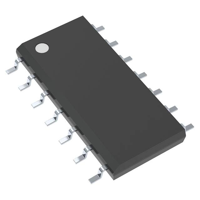
SOIC−14 NB
CASE 751A
XXXXX
A
WL
Y
WW
G
1
= Specific Device Code
= Assembly Location
= Wafer Lot
= Year
= Work Week
= Pb−Free Package
PIN CONNECTIONS
TxD1
1
14
STB1
RxD1
2
13
CANH1
GND
3
12
CANL1
VCC
4
11
TEST/GND
GND
5
10
CANH2
RxD2
6
9
CANL2
TxD2
7
8
STB2
NCV7441
•
•
14
Dual CAN
• Compatible with the ISO 11898 Standard (ISO 11898−2, ISO
•
•
•
•
•
•
•
MARKING
DIAGRAM
14
Features
•
•
•
http://onsemi.com
Typical Applications
• Automotive
• Industrial Networks
© Semiconductor Components Industries, LLC, 2011
August, 2011 − Rev. 0
ORDERING INFORMATION
See detailed ordering and shipping information in the
package dimensions section on page 9 of this data sheet.
1
Publication Order Number:
NCV7441/D
�NCV7441
BLOCK DIAGRAM
VCC
NCV7441
Dual CAN
CANH1
CANH2
Transmitter
Transmitter
Receiver
CANL2
CHANNEL 2
CONTROL LOGIC
CHANNEL 1
CONTROL LOGIC
CANL1
SUPPLY
MONITOR
Receiver
THERMAL
MONITOR
Low−power
receiver
VCC
Low −power
receiver
VCC
VCC
VCC
GND
STB2
TxD2
RxD2
TEST/
GND
RxD1
TxD1
STB1
PD20100615.01
Figure 1. NCV7441 Dual CAN: Block Diagram
Table 1. PIN FUNCTION DESCRIPTION
Pin
Number
Pin
Name
Pin Type
Description
transmit data for the
mode
1st
1
TxD1
digital input;
internal pull−up
CAN channel in normal mode; ignored in standby
2
RxD1
digital output
3
GND
ground
4
VCC
supply input
5
GND
ground
6
RxD2
digital output
7
TxD2
digital input;
internal pull−up
transmit data for the 2nd CAN channel
8
STB2
digital input;
internal pull−up
mode control input for the 2nd CAN channel; STB2 = High puts the 2nd CAN
channel into standby mode
9
CANL2
high−voltage analog
input/output
CANL−wire connection of the 2nd CAN channel
10
CANH2
high−voltage analog
input/output
CANH−wire connection of the 2nd CAN channel
11
TEST /
GND
test/ground
12
CANL1
high−voltage analog
input/output
CANL−wire connection of the 1st CAN channel
13
CANH1
high−voltage analog
input/output
CANH−wire connection of the 1st CAN channel
14
STB1
digital input;
internal pull−up
received data from the 1st CAN channel in normal mode; 1st CAN channel
remote wakeup indication in standby mode
ground connection
5 V supply connection
ground connection
received data from the 2nd CAN channel; 2nd CAN channel remote wakeup
indication in standby mode
The pin is used for test purposes during device production. It’s recommended
to connect to ground in the end−application.
mode control input for the 1st CAN channel;
STB1 = High puts the 1st CAN channel into standby mode
http://onsemi.com
2
�NCV7441
TYPICAL APPLICATION DIAGRAM
LDO
5V
VCC
STB1
MCU + CAN ctrl.
CANH1
TxD1
1
CANL1
RxD1
NCV7441−0
Dual CAN
STB2
MCU + CAN ctrl.
CANH2
TxD2
CANL2
RxD2
TEST/
GND
GND
GND
CAN2
2
CAN1
VBAT
PD20100615.03
Figure 2. NCV7441 Dual CAN: Example Application Diagram
FUNCTIONAL DESCRIPTION
Dual CAN device behaves identically to two independent CAN transceivers. The representative signal dependencies are
shown in Figure 4 and further functional description is given in Table 2.
Table 2. FUNCTIONAL DESCRIPTION
VCC
STB1/2
TxD1/2
RxD1/2
Transceiver on CANH1/2/CANL1/2
< VCC_UV
X
X
HZ
> VCC_UV
High
X
Low−power receiver
output
Transmitter deactivated;
Bus biased to GND through the input circuitry;
Receiver monitoring CAN1/2 wakeup
CAN1/2 in standby
mode
Low
High
Indicates the signal
received on CAN1/2
Recessive signal transmitted on CAN1/2;
Bus biased to VCC/2 through the input circuitry
CAN1/2 in normal
mode
Low
Low
Deactivated; unbiased
Dominant signal transmitted on CAN1/2;
Bus biased to VCC/2 through the input circuitry
http://onsemi.com
3
Comment
The entire chip in
under−voltage
�NCV7441
If the main power supply VCC (nominal 5 V) is above its under−voltage (VCC_UV) level, each CAN channel can enter either
normal mode (when the corresponding STB1/2 digital input is pulled Low) or standby mode (when the corresponding STB1/2
signal is left High):
• In the normal mode:
♦ The bus transceiver is ready to transmit and receive CAN bus signals with the full CAN communication speed (up to
1 Mbps) and thus interconnect the CAN bus with the corresponding CAN controller through digital pins TxD1/2 and
RxD1/2
♦ The bus pins are internally biased to typically VCC/2 through the input circuitry
♦ TxD1/2 input pin is monitored by a timeout in order to prevent a permanent dominant being forced to the bus thus
preventing other nodes from communicating. If TxD1/2 is Low for longer than tcnt(timeout), the transmitter switches
back to recessive. Only when TxD1/2 returns to High, the timeout counter is reset and the transmitter is ready to
transmit dominant symbols again. The TxD1/2 timeout protection is implemented individually for both CAN
transceivers.
♦ A common thermal monitoring circuit compares the circuit junction temperatures with threshold TJ(sd). If the thermal
shutdown level is exceeded, dominant transmission is disabled. The circuit remains biased and ready to transmit but
the logical path from TxD1/2 pin(s) is blocked. The transmission is again enabled when the junction temperature
decreases below the shutdown level and the TxD1/2 pin returns to the High level, thus avoiding thermal oscillations.
• In the standby mode:
♦ The respective transmitter is disabled and the current consumption of the channel is fundamentally reduced. Only the
low−power receiver on the channel remains active in order to detect potential CAN bus wakeups. The logical signal
on TxD1/2 input is ignored.
♦ The bus pins are biased to GND through the input circuitry
♦ Digital output RxD1/2 signals the output of the low−power receiver and can be used as a wakeup signal in the
application. A filtering time tdBUS is applied between the bus activity and the RxD1/2 signal in order to ensure that
only sufficiently long dominant signals on the bus will be propagated to the digital output. In addition, dominant bus
signals are ignored in case they were present during normal−to−standby mode transition; in this way unwanted
wakeups are avoided in case of permanent dominant failure on the bus. Example waveforms illustrating bus activity
detection in standby mode are shown in Figure 3.
In order to ensure a safe device state, the digital inputs STB1/2 and TxD1/2 are connected through internal pull−up resistors
to VCC thus ensuring that both channels remain in standby mode and/or no dominant can be transmitted in case any of the digital
inputs gets disconnected.
STB1
< tdbus
wtdbus
wtdbus
< t dbus
CANH/L1
RxD1
STB2
< tdbus
CANH/L2
RxD2
PD20100209.08
Figure 3. NCV7441 Dual CAN: Bus Activity Detection in Standby Mode
http://onsemi.com
4
wtdbus
�5
http://onsemi.com
RxD2
CANH/L2
STB2
TxD2
RxD1
CANH/L1
STB1
TxD1
PD20100209.03
Re mo te
wakeup
Legend:
received
dominant
transmitted
dominant
Re mo te
wakeup
NCV7441
Figure 4. NCV7441 Dual CAN: Functional Graphs
�NCV7441
Table 3. ABSOLUTE MAXIMUM RATINGS
Min
Max
Unit
Vmax_VCC
Symbol
Supply voltage
−0.3
6
V
Vmax_digIn
Voltage at digital inputs. TxD1, TxD2, STB1, STB2
−0.3
6
V
Vmax_digOut
Voltage at digital outputs. RxD1, RxD2, TEST/GND
−0.3
(VCC
+ 0.3)
V
Vmax_CANH1/2
Voltage on CANH1/2 pin; no time limit
−50
+50
V
Vmax_CANL1/2
Voltage on CANL1/2 pin ; no time limit
−50
+50
V
Vmax_diffCAN
Absolute voltage difference between CAN pins: |V(CANH1)−V(CANL1)|;
|V(CANH2)−V(CANL2)|
0
50
V
Junction temperature
−40
170
°C
System ESD on CANH1/2 and CANL1/2 as per IEC 61000−4−2: 330 W / 150 pF
−8
8
kV
Human body model on CANH1/2 and CANL1/2 as per JESD22−A114 / AEC−
Q100−002
−8
8
kV
Human body model on other pins as per JESD22−A114 / AEC−Q100−002
−4
4
kV
Charge device model on all pins as per JESD22−C101 / AEC−Q100−011
−500
500
V
TJ(max)
ESD
Parameter
Stresses exceeding Maximum Ratings may damage the device. Maximum Ratings are stress ratings only. Functional operation above the
Recommended Operating Conditions is not implied. Extended exposure to stresses above the Recommended Operating Conditions may affect
device reliability.
Table 4. OPERATING RANGES
Symbol
Parameter
Min
Max
Unit
4.75
5.25
V
Vop_VCC
Supply voltage
Vop_digIn
Voltage at digital inputs. Dual CAN: TxD1, TxD2, STB1, STB2
0
VCC
V
Voltage at digital outputs. RxD1, RxD2
0
VCC
V
Vop_digOut
Vop_CANH1/2
Voltage on CANH1/2 pin
Guaranteed receiver function
−35
35
V
Vop_CANL1/2
Voltage on CANL1/2 pin
Guaranteed receiver function
35
35
V
Vop_diffCAN
Absolute voltage difference between CAN pins:
|V(CANH1) − V(CANL1)|; |V(CANH2) − V(CANL2)|
Guaranteed receiver function
0
35
V
−40
150
°C
TJ_op
Junction temperature
http://onsemi.com
6
�NCV7441
Table 5. ELECTRICAL CHARACTERISTICS
The characteristics defined in this section are guaranteed within the operating ranges listed in Figure 4, unless stated otherwise. Positive
currents flow into the respective pin.
Symbol
Parameter
Conditions
Min
Typ
Max
Unit
2.5
3.5
4.5
V
20
30
mA
VCC SUPPLY ELECTRICAL CHARACTERISTICS
VCC_UV
IVCC_stdby
VCC under voltage level
VCC consumption
Both channels in standby mode;
no wakeup detected;
both buses recessive
TxD1 = TxD2 = High
IVCC_norm1
One channel in normal mode;
TxD1 = TxD2 = High
3
5
11
mA
IVCC_norm2
Both channels in normal mode;
TxD1 = TxD2 = High
6
10
20
mA
DIGITAL INPUTS ELECTRICAL CHARACTERISTICS – PINS TxD1, TxD2
VTxX_L
Low level input voltage
−0.3
0.8
V
VTxX_H
High level input voltage
2
VCC +
0.3
V
ITxX_L
Low level input current
VCC = 5 V
V(TxX) = GND
−75
−350
mA
ITxX_H
High level input current
VCC = 0 ... 5.25 V
V(TxX) = 5 V
−0.5
0.5
mA
−200
DIGITAL INPUTS ELECTRICAL CHARACTERISTICS – PINS STB1, STB2
VSTBX_L
Low level input voltage
−0.3
0.8
V
VSTBX_H
High level input voltage
2
VCC +
0.3
V
ISTBX_L
Low level input current
VCC = 5 V
V(STBX) = GND
−1
−10
mA
ISTBX_H
High level input current
VCC = 0 ... 5.25 V
V(STBX) = 5 V
−0.5
0.5
mA
−4
DIGITAL OUTPUTS ELECTRICAL CHARACTERISTICS – PINS RxD1, RxD2
IdigOut_L
Output current at Low output level
V(digOut) = 0.4 V
2
6
12
mA
IdigOut_H
Output current at High output level
at least one channel enabled
V(digOut) = VCC − 0.4 V
−0.1
−0.4
−1
mA
Output level in standby
mode
both channels in standby;
I(digOut) = −100 mA
VCC −
1.1
VCC −
0.7
VCC −
0.4
V
Output current in High−impedance state
during VCC undervoltage;
V(digOut) = 0 V ... VCC
−2
0
2
mA
VTxD1/2 = VCC;
no load on the bus, normal mode
2.0
2.5
3.0
V
no load on the bus;
standby mode
−0.1
0
0.1
VTxD1/2 = VCC;
no load on the bus, normal mode
2.0
2.5
3.0
no load on the bus;
standby mode
−0.1
0
0.1
VdigOut_stdby
IdigOut_HZ
CAN TRANSMITTER CHARACTERISTICS
Vo(reces)(CANH1/2)
Vo(reces)(CANL1/2)
recessive bus voltage at
pin CANH1/2
recessive bus voltage at
pin CANL1/2
V
Io(reces)(CANH1/2)
recessive output current at
pin CANH1/2
−35 V < VCANH1/2 < 35 V;
0 V < VCC < 5.25 V
−2.5
−
2.5
mA
Io(reces)(CANL1/2)
recessive output current at
pin CANL1/2
−35 V < VCANL1/2 < 35 V;
0 V < VCC < 5.25 V
−2.5
−
2.5
mA
http://onsemi.com
7
�NCV7441
Table 5. ELECTRICAL CHARACTERISTICS
The characteristics defined in this section are guaranteed within the operating ranges listed in Figure 4, unless stated otherwise. Positive
currents flow into the respective pin.
Symbol
Parameter
Conditions
Min
Typ
Max
Unit
CAN TRANSMITTER CHARACTERISTICS
Vo(dom)(CANH1/2)
dominant output voltage at
pin CANH1/2
VTXD1/2 = 0 V
3.0
3.6
4.25
V
Vo(dom)(CANL1/2)
dominant output voltage at
pin CANL1/2
VTXD1/2 = 0 V
0.5
1.4
1.75
V
Vo(dif)(BUS_dom)
differential bus output
voltage
(VCANH1/2 – VCANL1/2)
VTXD1/2 = 0 V, dominant;
bus differential load:
42.5 W < RL < 60 W
1.5
2.25
3.0
V
Vo(dif)(BUS_rec)
differential bus output
voltage
(VCANH1/2 – VCANL1/2)
VTXD1/2 = VCC
Recessive,
no load on the bus
−120
0
50
mV
Io(SC)(CANH1/2)
short−circuit output current
at pin CANH1/2
VCANH1/2 = 0 V,
VTXD1/2 = 0 V
−100
−70
−45
mA
Io(SC)(CANL1/2)
short−circuit output current
at pin CANL1/2
VCANL1/2= 36 V,
VTXD1/2 = 0 V
45
70
100
mA
normal mode
−12 V < VCANH1/2 < 12 V
−12 V < VCANL1/2 < 12 V
0.5
0.7
0.9
V
standby mode
−12 V < VCANH1/2 < 12 V
−12 V < VCANL1/2 < 12 V
0.4
0.8
1.15
CAN RECEIVER AND CAN PINS ELECTRICAL CHARACTERISTICS
Vi(dif)(th)
Differential receiver
threshold voltage
Vihcm(dif)(th)
Differential receiver
threshold voltage for high
common mode
normal mode
−35 V < VCANH1/2 < 35 V
−35 V < VCANL1/2 < 35 V
0.4
0.7
1
V
Vihcm(dif)(hys)
Differential receiver input
voltage hysteresis for high
common mode
normal mode
−35 V < VCANH1/2 < 35 V
−35 V < VCANL1/2 < 35 V
20
70
100
mV
Ri(cm)CANH1/2
Common mode input resistance at pin CANH1/2
15
26
37
kW
Ri(cm)CANL1/2
Common mode input resistance at pin CANL1/2
15
26
37
kW
Ri(cm)(m)
Matching between pin
CANH1/2 and pin
CANL1/2 common mode
input resistance
−3
0
3
%
25
50
75
kW
VCANH1/2= VCANL1/2
Ri(dif)
Differential input resistance
CI(CANH1/2)
input capacitance at pin
CANH1/2
VTxD1/2 = VCC
not tested in production
−
7.5
20
pF
CI(CANL1/2)
input capacitance at pin
CANL1/2
VTxD1/2 = VCC
not tested in production
−
7.5
20
pF
CI(dif)
differential input capacitance
VTxD1/2 = VCC
not tested in production
−
3.75
10
pF
ILICANH1/2
Input leakage current to
pin CANH1/2
VCC = 0 V;
VCANL1/2 = VCANH1/2 = 5 V
−10
0
10
mA
ILICANL1/2
Input leakage current to
pin CANL1/2
VCC = 0 V;
VCANL1/2 = VCANH1/2 = 5 V
−10
0
10
mA
185
°C
THERMAL MONITORING ELECTRICAL CHARACTERISTICS
TJ(sd)
Thermal shutdown
threshold
Junction temperature rising
150
Junction temperature falling
145
http://onsemi.com
8
°C
�NCV7441
Table 5. ELECTRICAL CHARACTERISTICS
The characteristics defined in this section are guaranteed within the operating ranges listed in Figure 4, unless stated otherwise. Positive
currents flow into the respective pin.
Symbol
Parameter
Conditions
Min
Typ
Max
Unit
20
85
120
ns
30
105
ns
DYNAMIC ELECTRICAL CHARACTERISTICS
td(TXD1/2−BUSOn)
delay TxD1/2 to CAN1/2
bus active
bus differential load 100 pF/60 W
td(TXD1/2−BUSOff)
delay TxD1/2 to CAN1/2
bus inactive
bus differential load 100 pF/60 W
td(BUSOn−RXD1/2)
delay CAN1/2 bus active
to RxD1/2
CRxD1/2 = 15 pF
25
55
105
ns
td(BUSOff−RX0)
delay CAN1/2 bus inactive
to RxD1/2
CRxD1/2 = 15 pF
30
100
105
ns
tdPD(TXD1/2−RXD1/2)dr
propagation delay TxD1/2
to RxD1/2;
dominant−to−recessive
bus differential load 100 pF/60 W
30
245
ns
tdPD(TXD1/2−RXD1/2)rd
propagation delay TxD1/2
to RxD1/2;
recessive−to−dominant
bus differential load 100 pF/60 W
75
230
ns
tdBUS
low−power receiver filtering time
standby mode
Vdif(dom) > 1.4 V
0.5
2.5
5
ms
standby mode
Vdif(dom) > 1.2 V
0.5
3
5.8
tdWAKE
delay to flag bus wakeup;
time from CAN bus dominant start to RxDx falling
edge
standby mode; dominant longer than
tdBUS
10
ms
td(nrm−stb)
transition delay from
STB1/2 rising edge to
CAN1/2 standby mode
10
ms
td(stb−nrm)
transition delay from
STB1/2 falling edge to
CAN1/2 normal mode
10
ms
tcnt(timeout)
TxD1/2 dominant time out
VTXD1/2 = 0 V
300
650
1000
ms
IdigOut_HZ
Output current in High−impedance state
pins RxD1,2 during VCC under−voltage;
V(digOut) = 0 V ... VCC
−2
0
2
mA
ORDERING INFORMATION
Device
NCV7441D20G
Description
Temperature Range
Package
Shipping†
Dual HS−CAN Transceiver
*40°C to 125°C
SOIC−14
(Pb−Free)
55 Tube / Tray
NCV7441D20R2G
3000 / Tape & Reel
†For information on tape and reel specifications, including part orientation and tape sizes, please refer to our Tape and Reel Packaging
Specifications Brochure, BRD8011/D.
http://onsemi.com
9
�NCV7441
PACKAGE DIMENSIONS
SOIC−14 NB
CASE 751A−03
ISSUE K
D
A
B
14
8
NOTES:
1. DIMENSIONING AND TOLERANCING PER
ASME Y14.5M, 1994.
2. CONTROLLING DIMENSION: MILLIMETERS.
3. DIMENSION b DOES NOT INCLUDE DAMBAR
PROTRUSION. ALLOWABLE PROTRUSION
SHALL BE 0.13 TOTAL IN EXCESS OF AT
MAXIMUM MATERIAL CONDITION.
4. DIMENSIONS D AND E DO NOT INCLUDE
MOLD PROTRUSIONS.
5. MAXIMUM MOLD PROTRUSION 0.15 PER
SIDE.
A3
E
H
L
1
0.25
M
DETAIL A
7
B
13X
M
b
0.25
M
C A
S
B
S
DETAIL A
h
A
X 45 _
M
A1
e
DIM
A
A1
A3
b
D
E
e
H
h
L
M
C
SEATING
PLANE
MILLIMETERS
MIN
MAX
1.35
1.75
0.10
0.25
0.19
0.25
0.35
0.49
8.55
8.75
3.80
4.00
1.27 BSC
5.80
6.20
0.25
0.50
0.40
1.25
0_
7_
INCHES
MIN
MAX
0.054 0.068
0.004 0.010
0.008 0.010
0.014 0.019
0.337 0.344
0.150 0.157
0.050 BSC
0.228 0.244
0.010 0.019
0.016 0.049
0_
7_
SOLDERING FOOTPRINT*
6.50
14X
1.18
1
1.27
PITCH
14X
0.58
DIMENSIONS: MILLIMETERS
*For additional information on our Pb−Free strategy and soldering
details, please download the ON Semiconductor Soldering and
Mounting Techniques Reference Manual, SOLDERRM/D.
ON Semiconductor and
are registered trademarks of Semiconductor Components Industries, LLC (SCILLC). SCILLC reserves the right to make changes without further notice
to any products herein. SCILLC makes no warranty, representation or guarantee regarding the suitability of its products for any particular purpose, nor does SCILLC assume any liability
arising out of the application or use of any product or circuit, and specifically disclaims any and all liability, including without limitation special, consequential or incidental damages.
“Typical” parameters which may be provided in SCILLC data sheets and/or specifications can and do vary in different applications and actual performance may vary over time. All
operating parameters, including “Typicals” must be validated for each customer application by customer’s technical experts. SCILLC does not convey any license under its patent rights
nor the rights of others. SCILLC products are not designed, intended, or authorized for use as components in systems intended for surgical implant into the body, or other applications
intended to support or sustain life, or for any other application in which the failure of the SCILLC product could create a situation where personal injury or death may occur. Should
Buyer purchase or use SCILLC products for any such unintended or unauthorized application, Buyer shall indemnify and hold SCILLC and its officers, employees, subsidiaries, affiliates,
and distributors harmless against all claims, costs, damages, and expenses, and reasonable attorney fees arising out of, directly or indirectly, any claim of personal injury or death
associated with such unintended or unauthorized use, even if such claim alleges that SCILLC was negligent regarding the design or manufacture of the part. SCILLC is an Equal
Opportunity/Affirmative Action Employer. This literature is subject to all applicable copyright laws and is not for resale in any manner.
PUBLICATION ORDERING INFORMATION
LITERATURE FULFILLMENT:
Literature Distribution Center for ON Semiconductor
P.O. Box 5163, Denver, Colorado 80217 USA
Phone: 303−675−2175 or 800−344−3860 Toll Free USA/Canada
Fax: 303−675−2176 or 800−344−3867 Toll Free USA/Canada
Email: orderlit@onsemi.com
N. American Technical Support: 800−282−9855 Toll Free
USA/Canada
Europe, Middle East and Africa Technical Support:
Phone: 421 33 790 2910
Japan Customer Focus Center
Phone: 81−3−5773−3850
http://onsemi.com
10
ON Semiconductor Website: www.onsemi.com
Order Literature: http://www.onsemi.com/orderlit
For additional information, please contact your local
Sales Representative
NCV7441/D
�


 工商网监
湘ICP备2023018690号
工商网监
湘ICP备2023018690号
