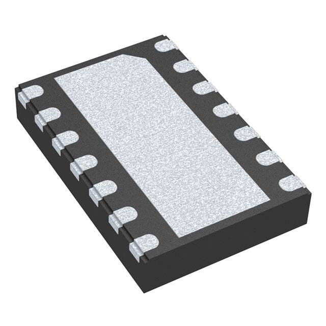
Dual CAN FD Transceiver,
High Speed, Low Power
NCV7446
Description
NCV7446 is a dual CAN FD physical layer transceiver. It allows
interfacing of two independent CAN physical buses and two
independent CAN protocol controllers. The transceivers provide
differential transmit capability to the bus and differential receive
capability to the CAN controllers.
It is consisted of two fully independent NCV7344 transceivers. The
NCV7446 guarantees additional timing parameters to ensure robust
communication at data rates beyond 1 Mbps to cope with CAN
flexible data rate requirements (CAN FD). These features make the
NCV7446 an excellent choice for all types of HS−CAN networks, in
nodes that require a low−power mode with wake−up capability via the
CAN bus.
Features
•
•
•
•
Quality
• Wettable Flank Package for Enhanced Optical Inspection
• AEC−Q100 Qualified and PPAP Capable
• These Devices are Pb−Free, Halogen Free/BFR Free and are RoHS
Compliant
MARKING
DIAGRAM
NV74
46−0
ALYW
G
1
DFNW14
CASE 507AC
NV7446−0 = Specific Device Code
A
= Assembly Site
L
= Wafer Lot
Y
= Year of Production, Last Number
W
= Work Week Number
G
= Pb−Free Package
PIN CONNECTIONS
TxD1
1
14
STB1
GND1
2
13
CANH1
VCC1
3
12
CANL1
RxD1
4
11
STB2
TxD2
5
10
CANH2
GND2
6
9
CANL2
VCC2
7
8
RxD2
NCV7446
•
•
•
•
•
•
•
Compliant with the ISO 11898−2:2016
CAN FD Timing Specified up to 5 Mbps
Very Low Current Standby Mode with Wake−up via the Bus
Low Electromagnetic Emission (EME) and High Electromagnetic
Immunity
No Disturbance of the Bus Lines with an Un−powered Node
Transmit Data (TxD) Dominant Timeout Function
Under All Supply Conditions the Chip Behaves Predictably
Very High ESD Robustness of Bus Pins
Thermal Protection
Bus Pins Short Circuit Proof to Supply Voltage and Ground
Bus Pins Protected Against Transients in an Automotive
Environment
www.onsemi.com
ORDERING INFORMATION
See detailed ordering and shipping information in the
package dimensions section on page 12 of this data sheet.
Typical Applications
• Automotive
• Industrial Networks
© Semiconductor Components Industries, LLC, 2018
December, 2019 − Rev. 2
1
Publication Order Number:
NCV7446/D
�NCV7446
BLOCK DIAGRAM
VCC1
3
NCV7446
V CC1
13
Thermal
TxD1
shutdown
1
CANH1
Timer
VCC 1
STB1
14
Mode &
Wake − up
12
Driver control
CANL1
control
RxD1
GND1
4
Wake − up
Filter
COMP
2
COMP
Channel 1
TxD2
5
GND2
6
V CC2
7
Channel2
Figure 1. NCV7446 Block Diagram
www.onsemi.com
2
11
STB2
10
9
CANH 2
CANL2
8
RxD2
�NCV7446
TYPICAL APPLICATION DIAGRAM
VBAT
IN
5V −reg
OUT
VCC
VCC1
VCC2
3
STB1
TxD1
RxD1
.
STB2
TxD2
RxD2
13
14
CANH1
CAN
BUS
1
4
12
NCV7446
Micro−
controller
7
11
10
CANL1
CANH2
CAN
BUS
5
8
9
2
6
GND1
GND
CANL2
GND2
Figure 2. NCV7446 Application Diagram
Table 1. PIN FUNCTION DESCRIPTION
Pin Number
Pin Name
1
TxD1
Transmit data input for channel 1; low input Ù dominant driver; internal pull−up current
Description
2
GND1
Ground for channel 1
3
VCC1
Supply voltage for channel 1
4
RxD1
Receive data output for channel 1; dominant transmitter Ù low output
5
TxD2
Transmit data input for channel 2; low input Ù dominant driver; internal pull−up current
6
GND2
Ground for channel 2
7
VCC2
Supply voltage for channel 2
8
RxD2
Receive data output for channel 2; dominant transmitter Ù low output
9
CANL2
Low−level CAN bus line channel 2 (low in dominant mode)
10
CANH2
High−level CAN bus line channel 2 (high in dominant mode)
11
STB2
Standby mode control input for channel 2; internal pull−up current
12
CANL1
Low−level CAN bus line channel 1 (low in dominant mode)
13
CANH1
High−level CAN bus line channel 1 (high in dominant mode)
14
STB1
EP
Exposed Pad
Standby mode control input for channel 1; internal pull−up current
Recommended to connect to GND or left floating in application
www.onsemi.com
3
�NCV7446
FUNCTIONAL DESCRIPTION
Operating Modes
Standby Mode
NCV7446 provides two modes of operation per
transceiver as illustrated in Table 2. These modes are
selectable through pins STB1 and STB2 independently for
each transceiver.
In standby mode both the transmitter and receiver are
disabled and a very low−power differential receiver
monitors the bus lines for CAN bus activity. The bus lines
are biased to ground and supply current is reduced to a
minimum. When a wake−up request is detected by the
low−power differential receiver, the signal is first filtered
and then verified as a valid wake signal after a time period of
twake_filt, the corresponding RxDx pin is driven low by the
transceiver (following the bus) to inform the controller of
the wake−up request.
Table 2. OPERATING MODES
Pins
STBx
Mode
Low
Normal
Low when bus
dominant
High when bus
recessive
High
Standby
Follows the bus
when wake−up
detected
High when no
wake−up request detected
Pins RxDx
Wake−up
When a valid wake−up pattern (phase in order
dominant − recessive − dominant) is detected during the
standby mode the RxDx pins follows the bus. Minimum
length of each phase is twake_filt – see Figure 3.
Pattern must be received within twake_to to be recognized
as valid wake−up otherwise internal logic is reset.
Normal Mode
In the normal mode, the selected transceiver is able to
communicate via the bus lines. The signals are transmitted
and received to the CAN controller via the pins TxDx and
RxDx. The slopes on the bus lines outputs are optimized to
give low EME.
twake_filt
twake_filt
twake_filt
CANHx
CANLx
< twake_to
tdwakerd tdwakedr
RxDx
Figure 3. NCV7446 Wake−up behavior
www.onsemi.com
4
�NCV7446
Overtemperature Detection
This TxD dominant timeout time tdom(TxD) defines
the minimum possible bit rate to 17 kbps.
A thermal protection circuit protects the IC from damage
by switching off the affected transmitter if the junction
temperature exceeds a value of approximately 170°C.
Because the transmitter dissipates most of the power, the
power dissipation and temperature of the IC is reduced. All
other IC functions continue to operate. The transmitter
off−state resets when the temperature decreases below
the shutdown threshold and pins TxDx goes high.
The thermal protection circuit is particularly needed when
a bus line short circuits.
Fail Safe Features
A current−limiting circuit protects the transmitter output
stage from damage caused by accidental short circuit
to either positive or negative supply voltage, although
power dissipation increases during this fault condition.
Undervoltage on VCC1 or VCC2 pins prevents the chip
sending data on the bus when there is not enough VCC supply
voltage.
After supply is recovered, corresponding TxD pin must be
first released to high to allow sending dominant bits again.
Recovery time from undervoltage detection is equal to
td(stb−nm) time.
The pins CANHx and CANLx are protected from
automotive electrical transients (according to ISO 7637; see
Figure 5). Pins TxDx and STBx are pulled high internally
should the input become disconnected. Pins TxDx, STBx
and RxDx will be floating, preventing reverse supply should
the adjacent VCCx supply be removed.
TxDx Dominant Timeout Function
A TxD dominant timeout timer circuit prevents the bus
lines being driven to a permanent dominant state (blocking
all network communication) if pins TxDx are forced
permanently low by a hardware and/or software application
failure. The timer is triggered by a negative edge on pins
TxDx. If the duration of the low−level on pins TxDx exceeds
the internal timer value tdom(TxD), the transmitter is
disabled, driving the bus into a recessive state. The timer is
reset by a positive edge on pins TxDx.
www.onsemi.com
5
�NCV7446
ELECTRICAL CHARACTERISTICS
Definitions
All voltages are referenced to GNDx (pin 2 or pin 6).
Positive currents flow into the IC. Sinking current means the
current is flowing into the pin; sourcing current means the
current is flowing out of the pin.
Table 3. ABSOLUTE MAXIMUM RATINGS
Symbol
Parameter
Conditions
Min
Max
Unit
VSUP
Supply voltage VCC1, VCC2
−0.3
+6
V
VCANH
DC voltage at pins CANHx
0 < VCCX < 5.25 V; no time limit
−42
+42
V
VCANL
DC voltage at pins CANLx
0 < VCCX < 5.25 V; no time limit
−42
+42
V
DC voltage between any two pins
(including CANHx and CANLx)
−42
+42
V
DC Voltage at pins TxDx, STBx
−0.3
+6
V
DC Voltage at pin RxDx
−0.3
VCCx + 0.3
V
VCANH−CANL
VIN
VOUT
VesdHBM
Electrostatic discharge voltage at all pins,
Component HBM
(Note 1)
−8
+8
kV
VesdCDM
Electrostatic discharge voltage at all pins,
Component CDM
(Note 2)
−750
+750
V
VesdIEC
Electrostatic discharge voltage at pins CANHx
and CANLx, System HBM (Note 4)
Without bus filter (Note 3)
−7
+7
kV
With bus filter (Note 3)
−11
+11
kV
Voltage transients, pins CANHx, CANLx.
According to ISO7637−3, Class C (Note 4)
test pulses 1
Vschaff
−100
test pulses 2a
+75
test pulses 3a
Latch−up
V
Static latch−up at all pins
−150
V
V
test pulses 3b
+100
V
(Note 5)
150
mA
Tstg
Storage temperature
−55
+150
°C
TJ
Maximum junction temperature
−40
+170
°C
MSL
Moisture Sensitivity Level
1
TSLD
Lead temperature Soldering − Reflow (Note 11)
−
−
260
°C
Stresses exceeding those listed in the Maximum Ratings table may damage the device. If any of these limits are exceeded, device functionality
should not be assumed, damage may occur and reliability may be affected.
1. Standardized human body model electrostatic discharge (ESD) pulses in accordance to EIA−JESD22. Equivalent to discharging a 100 pF
capacitor through a 1.5 kW resistor.
2. Standardized charged device model ESD pulses when tested according to AEC−Q100−011.
3. System human body model electrostatic discharge (ESD) pulses in accordance to IEC 61000−4−2. Equivalent to discharging a 150 pF
capacitor through a 330 W resistor referenced to GNDx.
4. Results were verified by external test house.
5. Static latch−up immunity: Static latch−up protection level when tested according to EIA/JESD78.
6. For information, please refer to our Soldering and Mounting Techniques Reference Manual, SOLDERRM/D
Table 4. THERMAL CHARACTERISTICS
Symbol
Parameter
Conditions
Value
Unit
RqJA_1
Thermal Resistance Junction−to−Air, JEDEC 1S0P PCB
Free air; (Note 8)
101
K/W
RqJA_2
Thermal Resistance Junction−to−Air, JEDEC 2S2P PCB
Free air; (Note 9)
53
K/W
RqJA_3
Thermal Resistance Junction−to−Air
Free air; (Note 10)
76
K/W
RqJA_4
Thermal Resistance Junction−to−Air
Free air; (Note 11)
46
K/W
7. Refer to ELECTRICAL CHARACTERISTICS, RECOMMENDED OPERATING RANGES and/or APPLICATION INFORMATION for Safe
Operating parameters.
8. Test board according to EIA/JEDEC Standard JESD51−3, signal layer with 10% trace coverage.
9. Test board according to EIA/JEDEC Standard JESD51−7, signal layers with 10% trace coverage.
10. Test board according to EIA/JEDEC Standard JESD51−3 and JESD51−5 , signal layer with 10% trace coverage and with thermal via array
under the exposed pad connected to the second copper layer.
11. Test board according to EIA/JEDEC Standard JESD51−5 and JESD51−7, signal layers with 10% trace coverage and thermal via array under
the exposed pad connected to the first inner copper layer.
www.onsemi.com
6
�NCV7446
Table 5. ELECTRICAL CHARACTERISTICS
VCC1, VCC2 = 4.75 V to 5.25 V; TJ = −40°C to +150°C; RLT = 60 W, CLT = 100 pF, C1 not used, CRxD = 15 pF, unless specified otherwise.
Symbol
Parameter
Conditions
Min
Typ
Max
Unit
4.75
5.0
5.25
V
55
mA
SUPPLY (PINS VCCX)
VCCx
Power supply voltage
(Note 12)
ICCx
Supply current on single channel
Dominant; VTxDx = Low
20
45
Recessive; VTxDx = Low
1.9
5.0
10
mA
Normal mode, Dominant;
VTxDx = 0 V; one of bus wires
shorted; −3 V ≤ (VCANHx,
VCANLx) ≤ +18 V
2.0
−
105
mA
−
10
15
mA
ICCSx
Supply current in standby mode on
single channel
TJ ≤ 100°C, (Note 13)
VUVD(VCC)(stby)
Standby undervoltage detection VCCx pins
3.5
4.0
4.3
V
VUVD(VCC)(swoff)
Switch−off undervoltage detection VCCx pins
2.0
2.3
2.6
V
TRANSMITTER DATA INPUT (Pins TxDx)
VIH
High−level input voltage
Output recessive
2.0
−
−
V
VIL
Low−level input voltage
Output dominant
−
−
+0.8
V
IIH
High−level input current
VTxDx = VCCx
−5.0
0
+5.0
mA
IIL
Low−level input current
VTxDx = 0 V
−300
−150
−70
mA
Ci
Input capacitance
(Note 13)
−
5
10
pF
2.0
−
−
V
TRANSMITTER MODE SELECT (Pins STBx)
VIH
High−level input voltage
Standby mode
VIL
Low−level input voltage
Normal mode
−
−
+0.8
V
IIH
High−level input current
VSTBx = VCCx
−1.0
0
+1.0
mA
IIL
Low−level input current
VSTBx = 0 V
−15
−
−1.0
mA
Ci
Input capacitance
(Note 13)
−
5
10
pF
RECEIVER DATA OUTPUT (Pins RxDx)
IOH
High−level output current
Normal mode
VRxDx = VCCx – 0.4 V
−8.0
−3.0
−1.0
mA
IOL
Low−level output current
VRxDx = 0.4 V
1.0
6.0
12
mA
Recessive output current at pins
CANHx and CANLx
−27 V < VCANHx, VCANLx <
+32 V; Normal mode
−5.0
−
+5.0
mA
Input leakage current
0 W < R(VCCx to GNDx) <
1 MW; VCANLx = VCANHx = 5 V
−5.0
0
+5.0
mA
Vo(rec)(CANH)
Recessive output voltage at pins CANHx
Normal mode, VTxDx = High;
RLT and CLT not used
2.0
2.5
3.0
V
Vo(rec)(CANL)
Recessive output voltage at pins CANLx
Normal mode, VTxDx = High;
RLT and CLT not used
2.0
2.5
3.0
V
Vo(off)(CANH)
Recessive output voltage at pin CANHx
Standby mode; RLT and CLT
not used
−0.1
−
+0.1
V
Vo(off)(CANL)
Recessive output voltage at pin CANLx
Standby mode; RLT and CLT
not used
−0.1
−
+0.1
V
Vo(off)(CANL)
Differential bus output voltage
(VCANHx * VCANLx)
Standby mode; RLT and CLT
not used
−0.2
−
+0.2
V
Vo(dom)(CANH)
Dominant output voltage at pins CANHx
VTxDx = 0 V; t < tdom(TxD);
50 W < RLT < 65 W
2.75
3.5
4.5
V
Vo(dom)(CANL)
Dominant output voltage at pins CANLx
VTxDx = 0 V; t < tdom(TxD);
50 W < RLT < 65 W
0.5
1.5
2.25
V
BUS LINES (Pins CANHx and CANLx)
Io(rec)
ILI
www.onsemi.com
7
�NCV7446
Table 5. ELECTRICAL CHARACTERISTICS
VCC1, VCC2 = 4.75 V to 5.25 V; TJ = −40°C to +150°C; RLT = 60 W, CLT = 100 pF, C1 not used, CRxD = 15 pF, unless specified otherwise.
Symbol
Parameter
Conditions
Min
Typ
Max
Unit
BUS LINES (Pins CANHx and CANLx)
Vo(dom)(diff)
Differential bus output voltage
(VCANHx − VCANLx)
VTxDx = 0 V; dominant;
45 W < RLT < 65 W
1.5
2.25
3.0
V
Vo(rec)(diff)
Differential bus output voltage
(VCANHx − VCANLx)
VTxDx = High; recessive; no
load
−50
0
+50
mV
Differential bus output voltage during
arbitration (VCANHx − VCANLx)
RLT = 2.24kW (Note 13)
1.5
−
5.0
V
Vo(dom)(sym)
Dominant output voltage driver symmetry
(VCANHx + VCANLx)
RLT = 60W; C1 = 4.7 nF; CLT
not used; TxDx = square
wave up to 1 MHz
0.9
1.0
1.1
VCCx
Io(sc)(CANH)
Short circuit output current at pins CANHx
−3 V < VCANHx < +18 V
−100
−
1.5
mA
Io(sc)(CANL)
Short circuit output current at pins CANLx
−3 V < VCANLx < +36 V
−1.5
−
100
mA
Vi(rec)(diff)_NM
Differential input voltage range recessive
state
Normal mode;
−12 V ≤ VCANHx,
VCANLx ≤ +12 V; no load
−3.0
−
0.5
V
Standby mode;
−12 V ≤ VCANHx,
VCANLx ≤ +12 V; no load
−3.0
0.4
V
Normal mode;
−12 V ≤ VCANHx,
VCANLx ≤ +12 V; no load
0.9
8.0
V
Standby mode;
−12 V ≤ VCANHx,
VCANLx ≤ +12 V; no load
1.05
8.0
V
Vo(dom)(diff)_arb
Vi(rec)(diff)_LP
Vi(dom)(diff)_NM
Differential input voltage range dominant
state
Vi(dom)(diff)_LP
−
Vi(diff)(th)_NORM
Differential receiver threshold voltage in
normal mode
−12 V ≤ VCANLx ≤ +12 V;
−12 V ≤ VCANHx ≤ +12 V
0.5
−
0.9
V
Vi(diff)(th)_NORM_H
Differential receiver threshold voltage in
normal mode, extended range
−30 V < VCANLx < +35 V;
−30 V < VCANHx < +35 V
0.4
−
1.0
V
Vi(diff)(th)_STDBY
Differential receiver threshold voltage in
standby mode
−12 V ≤ VCANLx ≤ +12 V;
−12 V ≤ VCANHx ≤ +12 V
0.4
−
1.05
V
Ri(cm)(CANH)
Common−mode input resistance at pin
CANHx
−2 V ≤ VCANLx ≤ +7 V;
−2 V ≤ VCANHx ≤ +7 V
15
26
37
kW
Ri(cm)(CANL)
Common−mode input resistance at pin
CANLx
−2 V ≤ VCANLx ≤ +7 V;
−2 V ≤ VCANHx ≤ +7 V
15
26
37
kW
Ri(cm)(m)
Matching between pin CANHx and pin
CANLx common mode input resistance
VCANHx = VCANLx = +5 V
−1
0
+1
%
Differential input resistance
−2 V ≤ VCANLx ≤ +7 V;
−2 V ≤ VCANHx ≤ +7 V
25
50
75
kW
Ci(CANH)
Input capacitance at pins CANHx
VTxDx = High; (Note 13)
−
4.5
20
pF
Ci(CANL)
Input capacitance at pins CANLx
VTxDx = High; (Note 13)
−
4.5
20
pF
Differential input capacitance
VTxDx = High; (Note 13)
−
3.75
10
pF
160
180
200
°C
Ri(diff)
Ci(diff)
THERMAL SHUTDOWN
TJ(sd)
Shutdown junction temperature per channel
Junction temperature rising
TIMING CHARACTERISTICS (see Figure 4 and Figure 6)
td(TxD−BUSon)
Delay TxDx to bus active
−
75
−
ns
td(TxD−BUSoff)
Delay TxDx to bus inactive
−
85
−
ns
td(BUSon−RxD)
Delay bus active to RxDx
−
24
−
ns
td(BUSoff−RxD)
Delay bus inactive to RxDx
−
32
−
ns
Propagation delay TxDx to RxDx
dominant to recessive transition
50
100
210
ns
tpd_dr
www.onsemi.com
8
�NCV7446
Table 5. ELECTRICAL CHARACTERISTICS
VCC1, VCC2 = 4.75 V to 5.25 V; TJ = −40°C to +150°C; RLT = 60 W, CLT = 100 pF, C1 not used, CRxD = 15 pF, unless specified otherwise.
Symbol
Parameter
Conditions
Min
Typ
Max
Unit
Propagation delay TxDx to RxDx
recessive to dominant transition
50
120
210
ns
td(stb−nm)
Delay standby mode to normal mode
5.0
11
20
ms
twake_filt
Dominant time for wake−up via bus
0.5
−
5.0
ms
tdwakerd
Delay to flag wake event
(recessive to dominant transitions)
Valid bus wake−up event
0.5
2.6
6.0
ms
tdwakedr
Delay to flag wake event
(dominant to recessive transitions)
Valid bus wake−up event
0.5
2.6
6.0
ms
twake_to
Bus time for wake−up timeout
Standby mode
1.0
−
10
ms
tdom(TxD)
TxDx dominant time for timeout
VTxDx = 0 V; Normal mode
1.0
−
10
ms
tBit(RxD)
Bit time on RxDx pin
tBit(TxD) = 500 ns
400
−
550
ns
tBit(TxD) = 200 ns
120
−
220
ns
tBit(TxD) = 500 ns
435
−
530
ns
tBit(TxD) = 200 ns
155
−
210
ns
tBit(TxD) = 500 ns
−65
−
+40
ns
tBit(TxD) = 200 ns
−45
−
+15
ns
TIMING CHARACTERISTICS (see Figure 4 and Figure 6)
tpd_rd
tBit(Vi(diff))
DtRec
Bit time on bus (CANHx – CANLx pin)
Receiver timing symmetry
DtRec = tBit(RxD) − tBit(Vi(diff));
12. In the range of 4.5 V to 4.75 V and from 5.25 V to 5.5 V the chip is fully functional; some parameters may be outside of the specification.
13. Values based on design and characterization, not tested in production.
MEASUREMENT SETUPS AND DEFINITIONS
0.7 × VIO
TxDx1
0.3 × VIO
0.3 × VIO
tbit(TxD)
td(TxD−BUSon)
5 × tbit(TxD)
Vi(diff)= VCANHx −VCANLx
tpd_rd
td(BUSon−RxD)
900 mV
500 mV
tbit(Vi(diff))
td(TxD−BUSoff)
td(BUSoff−RxD)
tpd_dr
0.7 × VIO
RxDx
0.3 × VIO
1
TxDx Edge length below 10 ns
Figure 4. Transceiver Timing Diagram
www.onsemi.com
9
tbit(RxD)
�NCV7446
+5 V
100 nF
VCC1
VCC2
3
TxD1
TxD2
RxD1
5
CANH1
1 nF
13
1
Transient
Generator
5
4
NCV7446
1 nF
12
15 pF
CANL1
CANH2
1 nF
10
RxD2
Transient
Generator
8
15 pF
1 nF
9
14
11
2
CANL2
6
STB1 STB2 GND1 GND2
Figure 5. Test Circuit for Automotive Transients
+5 V
100 nF
VCC1
V CC2
3
TxD 1
TxD2
RxD1
5
13
R LT /2
4.7 nF
1
5
4
NCV 7446
15 pF
C1
R LT /2
12
10
RxD 2
CANH 1
CANL 1
CANH2
8
9
14
11
2
6
C1
R LT /2
CANL 2
2x 30 W
STB1 STB2 GND 1 GND2
Figure 6. Test Circuit for Timing Characteristics
www.onsemi.com
10
100 pF
2x 30 W
R LT /2
4.7 nF
15 pF
C LT
C LT
100 pF
�NCV7446
Table 6. ISO 11898−2:2016 PARAMETER CROSS−REFERENCE TABLE
ISO 11898−2:2016 Specification
Parameter
NCV7446 Datasheet
Notation
Symbol
Single ended voltage on CAN_H
VCAN_H
Vo(dom)(CANH)
Single ended voltage on CAN_L
Dominant output characteristics
VCAN_L
Vo(dom)(CANL)
Differential voltage on normal bus load
VDiff
Vo(dom)(diff)
Differential voltage on effective resistance during arbitration
VDiff
Vo(dom)(diff)_arb
Differential voltage on extended bus load range (optional)
VDiff
Vo(dom)(diff)
VSYM
Vo(dom)(sym)
Absolute current on CAN_H
ICAN_H
Io(SC)(CANH)
Absolute current on CAN_L
ICAN_L
Io(SC)(CANL)
Single ended output voltage on CAN_H
VCAN_H
Vo(rec)(CANH)
Single ended output voltage on CAN_L
VCAN_L
Vo(rec)(CANL)
VDiff
Vo(rec)(diff)
Single ended output voltage on CAN_H
VCAN_H
Vo(off)(CANH)
Single ended output voltage on CAN_L
VCAN_L
Vo(off)(CANL)
VDiff
Vo(off)(dif)
Transmit dominant timeout, long
tdom
tdom(TxD)
Transmit dominant timeout, short
tdom
NA
Recessive state differential input voltage range
VDiff
Vi(rec)(diff)_NM
Dominant state differential input voltage range
VDiff
Vi(dom)(diff)_NM
Driver symmetry
Driver symmetry
Driver output current
Receiver output characteristics, bus biasing active
Differential output voltage
Receiver output characteristics, bus biasing inactive
Differential output voltage
Optional transmit dominant timeout
Static receiver input characteristics, bus biasing active
Static receiver input characteristics, bus biasing inactive
Recessive state differential input voltage range
VDiff
Vi(rec)(diff)_LP
Dominant state differential input voltage range
VDiff
Vi(dom)(diff)_LP
RDiff
Ri(diff)
RCAN_H
RCAN_L
Ri(cm)(CANH)
Ri(cm)(CANL)
mR
Ri(cm)(m)
tLoop
tpd_rd
tpd_dr
Receiver input resistance
Differential internal resistance
Single ended internal resistance
Receiver input resistance matching
Matching a of internal resistance
Implementation loop delay requirement
Loop delay
Optional implementation data signal timing requirements for use with bit rates above 1 Mbit/s and up to 2 Mbit/s
Transmitted recessive bit width @ 2 Mbit/s
tBit(Bus)
tBit(Vi(diff))
Received recessive bit width @ 2 Mbit/s
tBit(RXD)
tBit(RxD)
DtRec
DtRec
Receiver timing symmetry @ 2 Mbit/s
www.onsemi.com
11
�NCV7446
Table 6. ISO 11898−2:2016 PARAMETER CROSS−REFERENCE TABLE
ISO 11898−2:2016 Specification
Parameter
NCV7446 Datasheet
Notation
Symbol
Optional implementation data signal timing requirements for use with bit rates above 2 Mbit/s and up to 5 Mbit/s
Transmitted recessive bit width @ 5 Mbit/s
tBit(Bus)
tBit(Vi(diff))
Transmitted recessive bit width @ 5 Mbit/s
tBit(RXD)
tBit(RxD)
DtRec
DtRec
VDiff
VCANH−CANL
General maximum rating VCAN_H and VCAN_L
VCAN_H
VCAN_L
VCANH
VCANL
Optional: Extended maximum rating VCAN_H and VCAN_L
VCAN_H
VCAN_L
NA
ICAN_H
ICAN_L
ILI
CAN activity filter time, long
tFilter
twake_filt
CAN activity filter time, short
tFilter
NA
Wake−up timeout, short
tWake
NA
Wake−up timeout, long
tWake
twake_to
tSilence
NA
tBias
NA
Received recessive bit width @ 5 Mbit/s
Maximum ratings of VCAN_H, VCAN_L and VDiff
Maximum rating VDiff
Maximum leakage currents on CAN_H and CAN_L, unpowered
Leakage current on CAN_H, CAN_L
Bus biasing control timings
Timeout for bus inactivity (Required for selective wake−up implementation only)
Bus Bias reaction time (Required for selective wake−up implementation only)
ORDERING INFORMATION
Device
Description
Package
Shipping†
NCV7446MW0R2G
Dual CAN FD Transceiver, High Speed, Low Power
DFNW14
(Pb−Free)
5000 / Tape & Reel
†For information on tape and reel specifications, including part orientation and tape sizes, please refer to our Tape and Reel Packaging
Specifications Brochure, BRD8011/D.
www.onsemi.com
12
�MECHANICAL CASE OUTLINE
PACKAGE DIMENSIONS
DFNW14 4.5x3, 0.65P
CASE 507AC
ISSUE D
1
DATE 03 JUL 2018
SCALE 2:1
L
ÇÇÇÇ
ÇÇÇÇ
PIN ONE
REFERENCE
L3
A B
D
L3
L
ALTERNATE
CONSTRUCTION
E
DETAIL A
EXPOSED
COPPER
TOP VIEW
A
DETAIL B
0.10 C
0.08 C
NOTE 4
PLATING
A1
A4
C
C
DETAIL B
A3
SIDE VIEW
SEATING
PLANE
C
A4
DETAIL A
D2
14X
1
L
7
PLATED
SURFACES
L3
SECTION C−C
NOTES:
1. DIMENSIONS AND TOLERANCING PER
ASME Y14.5M, 1994.
2. CONTROLLING DIMENSION: MILLIMETERS.
3. DIMESNION b APPLIES TO PLATED
TERMINAL AND IS MEASURED BETWEEN
0.15 AND 0.30 MM FROM TERMINAL.
4. COPLANARITY APPLIES TO THE EXPOSED
PAD AS WELL AS THE TERMINALS.
5. THIS DEVICE CONTAINS WETTABLE FLANK
DESIGN FEATURES TO AID IN FILLET FORMATION ON THE LEADS DURING MOUNTING.
DIM
A
A1
A3
A4
b
D
D2
E
E2
e
K
L
L3
MILLIMETERS
MIN
NOM
MAX
0.80
0.85
0.90
−−−
−−−
0.05
0.20 REF
0.10
−−−
−−−
0.25
0.30
0.35
4.40
4.50
4.60
4.13
4.20
4.27
2.90
3.00
3.10
1.53
1.60
1.67
0.65 BSC
0.30 REF
0.35
0.40
0.45
0.00
0.05
0.10
GENERIC
MARKING DIAGRAM*
E2
K
8
14
14X
e
BOTTOM VIEW
b
0.10
M
C A B
0.05
M
C
NOTE 3
RECOMMENDED
SOLDERING FOOTPRINT*
14X
4.35
4.23
14
0.75
8
3.60 1.75
1
7
0.65
PITCH
XXXXX
XXXXX
AYWWG
G
XXXXX = Specific Device Code
A
= Assembly Location
Y
= Year
WW
= Work Week
G
= Pb−Free Package
(*Note: Microdot may be in either location)
*This information is generic. Please refer to
device data sheet for actual part marking.
Pb−Free indicator, “G” or microdot “ G”, may
or may not be present. Some products may
not follow the Generic Marking.
PACKAGE
OUTLINE
14X
0.33
DIMENSIONS: MILLIMETERS
*For additional information on our Pb−Free strategy and soldering
details, please download the ON Semiconductor Soldering and
Mounting Techniques Reference Manual, SOLDERRM/D.
DOCUMENT NUMBER:
DESCRIPTION:
98AON14979G
DFNW14 4.5x3, 0.65P
Electronic versions are uncontrolled except when accessed directly from the Document Repository.
Printed versions are uncontrolled except when stamped “CONTROLLED COPY” in red.
PAGE 1 OF 1
ON Semiconductor and
are trademarks of Semiconductor Components Industries, LLC dba ON Semiconductor or its subsidiaries in the United States and/or other countries.
ON Semiconductor reserves the right to make changes without further notice to any products herein. ON Semiconductor makes no warranty, representation or guarantee regarding
the suitability of its products for any particular purpose, nor does ON Semiconductor assume any liability arising out of the application or use of any product or circuit, and specifically
disclaims any and all liability, including without limitation special, consequential or incidental damages. ON Semiconductor does not convey any license under its patent rights nor the
rights of others.
© Semiconductor Components Industries, LLC, 2018
www.onsemi.com
�onsemi,
, and other names, marks, and brands are registered and/or common law trademarks of Semiconductor Components Industries, LLC dba “onsemi” or its affiliates
and/or subsidiaries in the United States and/or other countries. onsemi owns the rights to a number of patents, trademarks, copyrights, trade secrets, and other intellectual property.
A listing of onsemi’s product/patent coverage may be accessed at www.onsemi.com/site/pdf/Patent−Marking.pdf. onsemi reserves the right to make changes at any time to any
products or information herein, without notice. The information herein is provided “as−is” and onsemi makes no warranty, representation or guarantee regarding the accuracy of the
information, product features, availability, functionality, or suitability of its products for any particular purpose, nor does onsemi assume any liability arising out of the application or use
of any product or circuit, and specifically disclaims any and all liability, including without limitation special, consequential or incidental damages. Buyer is responsible for its products
and applications using onsemi products, including compliance with all laws, regulations and safety requirements or standards, regardless of any support or applications information
provided by onsemi. “Typical” parameters which may be provided in onsemi data sheets and/or specifications can and do vary in different applications and actual performance may
vary over time. All operating parameters, including “Typicals” must be validated for each customer application by customer’s technical experts. onsemi does not convey any license
under any of its intellectual property rights nor the rights of others. onsemi products are not designed, intended, or authorized for use as a critical component in life support systems
or any FDA Class 3 medical devices or medical devices with a same or similar classification in a foreign jurisdiction or any devices intended for implantation in the human body. Should
Buyer purchase or use onsemi products for any such unintended or unauthorized application, Buyer shall indemnify and hold onsemi and its officers, employees, subsidiaries, affiliates,
and distributors harmless against all claims, costs, damages, and expenses, and reasonable attorney fees arising out of, directly or indirectly, any claim of personal injury or death
associated with such unintended or unauthorized use, even if such claim alleges that onsemi was negligent regarding the design or manufacture of the part. onsemi is an Equal
Opportunity/Affirmative Action Employer. This literature is subject to all applicable copyright laws and is not for resale in any manner.
PUBLICATION ORDERING INFORMATION
LITERATURE FULFILLMENT:
Email Requests to: orderlit@onsemi.com
onsemi Website: www.onsemi.com
◊
TECHNICAL SUPPORT
North American Technical Support:
Voice Mail: 1 800−282−9855 Toll Free USA/Canada
Phone: 011 421 33 790 2910
Europe, Middle East and Africa Technical Support:
Phone: 00421 33 790 2910
For additional information, please contact your local Sales Representative
�