NCV7705(A), NCV7706
Mirror-Module Driver-IC
The NCV7705/NCV7706 is a powerful Driver−IC for automotive
body control systems. The IC is designed to control several loads in
the front door of a vehicle. The monolithic IC is able to control mirror
functions like mirror positioning, heating and folding. In addition,
NCV7706 includes the electro−chromic mirror feature. The device
features four high−side outputs to drive LEDs or incandescent bulbs
(up to 5/10 W). To allow maximum flexibility, all lighting outputs can
be PWM controlled thru PWM inputs (external signal source) or by an
internal programmable PWM generator unit. The
NCV7705/NCV7706 is controlled thru a 24 bit SPI interface with
in−frame response.
Features
• Operating Range from 5.5 V to 28 V
• Four High−Side and Four Low−Side Drivers Connected as
•
•
•
•
•
•
•
•
•
•
•
•
•
www.onsemi.com
SSOP36 EP
DQ SUFFIX
CASE 940AB
MARKING DIAGRAM
Half−Bridges
♦ 2x Half−bridges Iload = 0.75 A; RDS(on) = 1.6 W @ 25°C
♦ 2x Half−Bridges Iload = 3 A; RDS(on) = 300 mW @ 25°C
NCV770x
Four High−Side Lamp Drivers
FAWLYYWWG
♦ 2x LED; Iload = 0.3 A; RDS(on) = 1.4 W @ 25°C
♦ 1x 10 W; Configurable as LED Driver; Iload = 2.5 A;
RDS(on) = 300 mW @ 25°C
♦ 1x 5 W; Configurable as LED Driver; Iload = 1.25 A;
NCV770x = Specific Device Code
NCV770x = (x = 5, 5A or 6)
RDS(on) = 600 mW @ 25°C
F
= Fab Location (NCV7705A only)
1x High−Side Driver for Mirror Heating; Iload = 6 A;
A
= Assembly Location
RDS(on) = 100 mW @ 25°C
WL
= Wafer Lot
YY
= Year
Electro Chromic Mirror Control (NCV7706 Only)
WW
= Work Week
♦ 1x 6−Bit Selectable Output Voltage Controller
G
= Pb−Free Package
♦ 1x LS for EC Control; Iload = 0.75 A; RDS(on) = 1.6 W @ 25°C
Independent PWM Functionality for All Outputs
ORDERING INFORMATION
Integrated Programmable PWM Generator Unit for All Lamp Driver
Shipping†
Device
Package
Outputs
NCV7705DQR2G
♦ 7−bit / 10−bit Selectable Duty−cycle Setting Precision
SSOP36−EP
1500 / Tape &
Programmable Soft−start Function to Drive Loads with Higher
NCV7705DQAR2G
GREEN
Reel
Inrush Currents as Current Limitation Value
(Pb−Free)
NCV7706DQR2G*
Multiplex Current Sense Analog Output for Advanced Load
†For information on tape and reel specifications,
Monitoring
including part orientation and tape sizes, please
Very Low Current Consumption in Standby Mode
refer to our Tape and Reel Packaging Specification
Brochure, BRD8011/D.
Charge Pump Output to Control an External Reverse Polarity
* Contact local sales office for availability
Protection MOSFET
24−Bit SPI Interface for Output Control and Diagnostic
• SSOP36−EP Power Package
Protection Against Short−circuit, Overvoltage and
• This is a Pb−Free Device
Over−temperature
Typical Applications
Downwards Pin−to−Pin and SPI Registers Compatible
• De−centralized Door Electronic Systems
with NCV7707
• Body Control Units (BCUs)
AEC−Q100 Qualified and PPAP Compliant
© Semiconductor Components Industries, LLC, 2016
June, 2018 − Rev. 1
1
Publication Order Number:
NCV7705/D
�NCV7705(A), NCV7706
VS
CHP
NCV7705/06
Undervoltage
Lockout
VCC
SI
SCLK
CSB
SO
Diagnostic
Overvoltage
Lockout
Power −on Reset
Chargepump
short circuit
openload
overload
overtemperature
overvoltage
undervoltage
overload
VS
OUT1
CONTROL _0 Register
Driver
Interface
VS
CONTROL _1 Register
OUT2
CONTROL _2 Register
VS
OUT3
CONTROL _3 Register
VS
PWM _5/6 Register
VS
PWM
Unit
OUT4
PWM _7/8 Register
VS
STATUS _0 Register
OUT5
VS
STATUS _1 Register
OUT6
VS
STATUS _2 Register
OUT7
VS
CONFIG Register
OUT8
Special Function Register
VS
PWM1
PWM2
PWM1
OUT9
OUT9
ISOUT/
PWM2
MUX
6
GND
Figure 1. Block Diagram
www.onsemi.com
2
DAC
EC Control
ECON
ECFB
NCV7706 only
�NCV7705(A), NCV7706
Vbat
blinker
Switches
LED
VS
OUT8
CHP
NCV7705/06
SI
SCLK
Power −on Reset
ISOUT /
PWM2
Rs
PWM
CAN/LIN SBC
(NCV7462)
High−Side
Switch
(1.4 Ω)
Logic Control
High−Side
Switch
(1.6 Ω)
High−Side
Switch
(1.6 Ω)
High−Side
Switch
(0.3 Ω)
Low−Side
Switch
(0.3 Ω)
Low−Side
Switch
(1.6 Ω)
Low−Side
Switch
(1.6 Ω)
Low−Side
Switch
(0.3 Ω)
OUT 5
Protection :
short circuit
open load
over temperature
VS undervoltage
VS overvoltage
Current Sensing
High−Side
Switch
(0.3 Ω)
safety
light
High−Side
Switch
(0.3/1.4 Ω)
High−Side
Switch
(0.6/1.4 Ω)
Logic IN
PWM1
safety
light
10W
/LED
OUT6
footstep
light
5W
/LED
OUT7
PWM Generator Unit
CSB
mC
High−Side
Switch
(1.4 Ω)
Charge Pump
24−bit
Serial
Data
Interface
SO
LED
GND
High−Side
Switch
(0.1 Ω)
Low−Side
Switch
(1.6 Ω)
DAC
EC Control
VCC
OUT4
LIN
OUT3
(NCV7321)
LIN
OUT1
mirror
y−axis
ECON
ECFB
OUT8
OUT 9
mirror
defroster
mirror
x−axis
mirror
fold
CAN
OUT2
ECM
NCV7706 only
Figure 2. Application Diagram
NCV7705
GND
OUT9
OUT1
OUT2
OUT3
VS
VS
SI
ISOUT/PWM2
CSB
SO
VCC
SCLK
n.c.
VS
n.c.
n.c.
GND
NCV7706
1
36
18
19
GND
OUT9
OUT8
OUT7
VS
OUT6
OUT5
VS
VS
PWM1
CHP
VS/TEST
n.c.
n.c.
OUT4
n.c.
n.c.
GND
GND
OUT9
OUT1
OUT2
OUT3
VS
VS
SI
ISOUT/PWM2
CSB
SO
VCC
SCLK
n.c.
VS
n.c.
n.c.
GND
1
36
18
19
Figure 3. Pin Connections (Top View)
www.onsemi.com
3
GND
OUT9
OUT8
OUT7
ECFB
OUT6
OUT5
VS
VS
PWM1
CHP
ECON
n.c.
n.c.
OUT4
n.c.
n.c.
GND
�NCV7705(A), NCV7706
PIN FUNCTION DESCRIPTION
Pin No.
Pin Name
Pin Type
1
GND
Ground
2
OUT9
HS driver Output
3
OUT1
Half bridge driver Output
Mirror common Output
4
OUT2
Half bridge driver Output
Mirror x/y control Output
5
OUT3
Half bridge driver Output
Mirror x/y control Output
6
VS
Supply
Battery Supply Input (all VS pins have to be connected externally)
7
VS
Supply
Battery Supply Input (all VS pins have to be connected externally)
8
SI
Digital Input
9
ISOUT/PWM2
Digital Input /
Analog Output
10
CSB
Digital Input
11
SO
Digital Output
Description
Ground Supply (all GND pins have to be connected externally)
Heater Output (has to be connected externally to pin 35)
SPI interface Serial Data Input
PWM control Input / Current Sense Output. This pin is a bidirectional pin.
Depending on the selected multiplexer bits, an image of the instant current of
the corresponding HS stage can be read out.
This pin can also be used as PWM control input pin for OUT6 and OUT8.
SPI interface Chip Select
SPI interface Serial Data Output
12
VCC
Supply
13
SCLK
Digital Input
Logic Supply Input
14
n.c.
15
VS
16
n.c.
17
n.c.
18
GND
Ground
Ground Supply (all GND pins have to be connected externally)
19
GND
Ground
Ground Supply (all GND pins have to be connected externally)
20
n.c.
SPI interface Shift Clock
Not connected
Supply
Battery Supply Input (all VS pins have to be connected externally)
Not connected
Not connected
Not connected
21
n.c.
22
OUT4
Not connected
23
n.c.
Not connected
24
n.c.
Not connected
25
VS/TEST
(NCV7705 only)
Supply
ECON
(NCV7706 only)
ECM driver Output
26
CHP
Analog Output
27
PWM1
Digital Input
28
VS
Supply
Battery Supply Input (all VS pins have to be connected externally)
Battery Supply Input (all VS pins have to be connected externally)
Half bridge driver Output
Mirror Fold Output
Test Input, has to be connected to VS in application
Electrochromic mirror control DAC output. If the Electrochrome feature is
selected, this output controls an external Mosfet, otherwise it remains in
high−impedance state.
If the electrochrome feature is not used in the application and not selected via
SPI the pin can be connected to VS.
Reverse Polarity FET Control Output
PWM control Input for OUT1−4, OUT5/7, OUT9
29
VS
Supply
30
OUT5
HS driver Output
LED / Bulb Output
31
OUT6
HS driver Output
LED / Bulb Output
32
VS
(NCV7705 only)
Supply
ECFB
(NCV7706 only)
ECM Input / Output
33
OUT7
HS driver Output
LED Output
34
OUT8
HS driver Output
LED Output
35
OUT9
HS driver Output
Heater Output (has to be connected externally to pin 2)
GND
Ground
Ground Supply (all GND pins have to be connected externally)
Heat slug
Ground
Substrate; Heat slug has to be connected to all GND pins
36
Connect to VS pins externally (no power connection)
Electrochromic Mirror Feedback Input, Fast discharge transistor Output
www.onsemi.com
4
�NCV7705(A), NCV7706
ABSOLUTE MAXIMUM RATINGS
Symbol
Min
Max
Power supply voltage
− Continuous supply voltage
− Transient supply voltage (t < 500 ms, ”clamped load dump”)
−0.3
−0.3
28
40
VCC
Logic supply
−0.3
5.5
V
Vdig
DC voltage at all logic pins (SO, SI, SCLK, CSB, PWM1)
−0.3
VCC + 0.3
V
Current monitor output / PWM2 logic input
−0.3
VCC + 0.3
V
−25
Vs − 25
40
Vs + 15
V
Static output voltage (OUT1−9, ECON, ECFB)
−0.3
Vs + 0.3
V
OUT1/4 Output current
− TJ > 25°C
− TJ < 25°C
−5
−5.5
5
5.5
OUT2/3 Output current
− TJ > 25°C
− TJ < 25°C
−1.25
−1.35
1.35
1.35
Vs
Visout/pwm2
Vchp
Voutx,
Vecon, Vecfb
Iout1/4
Iout2/3
Iout5
Iout6
Iout7/8
Iout9
Rating
Charge pump output (the most stringent value is applied)
Unit
V
A
A
OUT5 Output current
− DC
− Transient
−5
A
OUT6 Output current
− DC
− Transient
−2.5
OUT7/8 Output current
− DC
− Transient
−1.25
5
A
2.5
A
1.25
OUT9 Output current
− DC
− Transient
A
−10
10
Iout_ecfb
(NCV7706
only)
ECFB Output current
1.25
ESD_HBM
ESD Voltage, Human Body Model (HBM); (100 pF, 1500 W) (Note 1)
− All pins
− Output pins OUT1−4 and ECFB to GND (all unzapped pins grounded)
A
kV
−2
−4
2
4
ESD according to CDM (Charge Device Model) (Note 1)
− All pins
− Corner pins
−500
−750
500
750
Operating junction temperature range
−40
150
°C
Tstg
Storage temperature range
−55
150
°C
MSL
Moisture sensitivity level (Note 2)
ESD_CDM
TJ
V
MSL3
Stresses exceeding those listed in the Maximum Ratings table may damage the device. If any of these limits are exceeded, device functionality
should not be assumed, damage may occur and reliability may be affected.
1. This device series incorporates ESD protection and is tested by the following methods:
ESD Human Body Model tested per AEC−Q100−002 (EIA/JESD22−A114)
ESD Charge Device Model tested per EIA/JES D22/C101, Field Induced Charge Model
2. For soldering information, please refer to our Soldering and Mounting Techniques Reference Manual, SOLDERRM/D
THERMAL CHARACTERISTICS
Symbol
Rating
Value
Unit
RθJA
Thermal Characteristics, SSOP36−EP, 1−layer PCB
Thermal Resistance, Junction−to−Air (Note 3)
49.4
°C/W
RθJA
Thermal Characteristics, SSOP36−EP, 4−layer PCB
Thermal Resistance, Junction−to−Air (Note 4)
24
°C/W
3. Values based on PCB of 76.2 x 114.3 mm, 72 μm copper thickness, 20% copper area coverage and FR4 PCB substrate.
4. Values based on PCB of 76.2 x 114.3 mm, 72 / 36 μm copper thickness (signal layers / internal planes), 20 / 90% copper area coverage (signal
layers / internal planes) and FR4 PCB substrate.
www.onsemi.com
5
�NCV7705(A), NCV7706
ELECTRICAL CHARACTERISTICS
4.5 V < VCC < 5.25 V, 8 V < Vs < 18 V, −40°C < TJ < 150°C; unless otherwise noted.
Symbol
Parameter
Test Conditions
Min
Typ
Max
Unit
28
18
V
3.5
12
mA
(9)
(25)
8
20
mA
4.5
6
mA
(15)
(50)
6.5
8
mA
8
18
mA
SUPPLY
Vs
Is(standby)
Is(active)
ICC(standby)
Supply voltage
Functional (see VUV_VS / VOV_VS)
Parameter specification
Supply Current (VS),
Standby mode
Standby mode,
VS = 16 V, 0 V v VCC v 5.25 V,
CSB = VCC, OUTx/ECx = floating,
SI = SCLK = 0 V, TJ < 85°C
(TJ = 150°C)
Supply current (VS),
Active mode
Active mode,
VS = 16 V,
OUTx/ECx = floating
Supply Current (VCC),
Standby mode
Standby mode,
VCC = 5.25 V,
SI = SCLK = 0 V, TJ < 85°C
(TJ = 150°C)
5.5
8
Active mode,
VS = 16 V,
OUTx/ECx = floating
ICC(active)
Supply current (VCC),
Active mode
I(standby)
Standby mode,
Total Standby mode supply current
VS = 16 V, TJ < 85°C,
(Is + ICC)
CSB = VCC, OUTx/ECx = floating
OVERVOLTAGE AND UNDERVOLTAGE DETECTION
Vuv_vs(on)
Vuv_vs(off)
Vuv_vs(hys)
VS Undervoltage detection
VS Undervoltage hysteresis
Vov_vs(off)
Vov_vs(on)
Vov_vs(hys)
VS Overvoltage detection
VS Overvoltage hysteresis
Vuv_vcc(off)
Vuv_vcc(on)
Vuv_vcc(hys)
VCC Undervoltage detection
VS increasing
5.6
6.2
V
VS decreasing
5.2
5.8
V
Vuv_vs(on) − Vuv_vs(off)
0.65
V
VS increasing
20
24.5
V
VS decreasing
19
23.5
V
Vov_vs(off) − Vov_vs(on)
2
VCC increasing
VCC decreasing
V
2.9
2
V
V
VCC Undervoltage hysteresis
Vuv_VCC(off) − Vuv_VCC(on)
0.11
V
td_uv
VS Undervoltage filter time
Time to set the power supply fail bit
UOV_OC in the Global Status Byte
6
13
ms
td_ov
VS Overvoltage filter time
Time to set the power supply fail bit
UOV_OC in the Global Status Byte
50
100
ms
CHARGE PUMP OUTPUT CHP
Vchp8
Chargepump Output Voltage
Vs = 8 V, Ichp = −60 mA
Vs + 6
Vs + 9.5
Vs + 13
V
Vchp10
Chargepump Output Voltage
Vs = 10 V, Ichp = −80 mA
Vs + 8
Vs + 11
Vs + 13
V
Vchp12
Chargepump Output Voltage
VS > 12 V, Ichp = −100 mA
Vs + 9.5
Vs + 11
Vs + 13
V
Ichp
Chargepump Output current
VS = 13.5 V, Vchp = Vs + 10 V
−95
mA
www.onsemi.com
6
−750
�NCV7705(A), NCV7706
ELECTRICAL CHARACTERISTICS (continued)
4.5 V < VCC < 5.25 V, 8 V < Vs < 18 V, −40°C < TJ < 150°C; unless otherwise noted.
Symbol
Parameter
Test Conditions
Min
Typ
Max
Unit
MIRROR COMMON OUTPUT (X/Y, FOLD) OUT1, OUT4
TJ = 25°C, Iout1,4 = ±1.5 A
0.3
W
Ron_out1,4
On−resistance HS or LS
Ioc1,4_hs
Overcurrent threshold HS
TJ < 25°C
TJ ≥ 25°C
−5.5
−5
−3
A
Ioc1,4_ls
Overcurrent threshold LS
TJ < 25°C
TJ ≥ 25°C
3
5.5
5
A
2
3
V
−5
mA
Vlim1,4
TJ = 125°C, Iout1,4 = ±1.5 A
Vds voltage limitation HS or LS
0.6
Iuld1,4_hs
Underload detection threshold HS
−80
Iuld1,4_ls
Underload detection threshold LS
5
td_HS1,4(on)
Output delay time, HS Driver on
td_HS1,4(off)
Output delay time, HS Driver off
td_LS1,4(on)
Output delay time, LS Driver on
td_LS1,4(off)
Output delay time, LS Driver off
80
mA
Time from CSB going high to
V(OUT1,4) = 0.1·Vs / 0.9·Vs (on/off)
2.5
12
ms
3
12
ms
Time from CSB going low to
V(OUT1,4) = 0.9·Vs / 0.1·Vs (on/off)
1
12
ms
1.5
12
ms
tdLH1,4
Cross conduction protection time,
low−to−high transition including LS
slew−rate
0.5
22
ms
tdHL1,4
Cross conduction protection time,
high−to−low transition including HS
slew−rate
5.5
22
ms
Ileak_act_hs1,4
Output HS leakage current,
Active mode
V(OUT1,4) = 0 V
Ileak_act_ls1,4
Output pull−down current,
Active mode
V(OUT1,4) = VS
Ileak_stdby_hs1,4
Output HS leakage current,
Standby mode
V(OUT1,4) = 0 V
Ileak_stdby_ls1,4
Output pull−down current,
Standby mode
V(OUT1,4) = VS, TJ w 25°C
V(OUT1,4) = VS, TJ < 25°C
td_uld1,4
Underload blanking delay
tdb_old1,4
Overload shutdown blanking delay Timer started after output activation
td_old1,4
Overload shutdown filter time
frec1,4L
−40
mA
−16
105
185
mA
mA
−5
120
175
mA
430
610
ms
16
25
ms
5
25
ms
Recovery frequency, slow recovery
CONTROL_3.OCRF = 0
mode
1
4
kHz
frec1,4H
Recovery frequency, fast recovery
mode
CONTROL_3.OCRF = 1
2
6
kHz
dVout1,4
Slew rate of HS driver
Vs = 13.5 V, Rload = 16 W to GND
3.3
V/ms
Timer started after blanking delay
elapsed
www.onsemi.com
7
80
1.3
2.3
�NCV7705(A), NCV7706
ELECTRICAL CHARACTERISTICS (continued)
4.5 V < VCC < 5.25 V, 8 V < Vs < 18 V, −40°C < TJ < 150°C; unless otherwise noted.
Symbol
Parameter
Test Conditions
Min
Typ
Max
Unit
MIRROR X/Y POSITIONING OUTPUTS OUT2, OUT3
TJ = 25°C, Iout2,3 = ±0.5 A
Ron_out2,3
On−resistance HS or LS
Ioc2,3_hs
Overcurrent threshold HS
TJ < 25°C
TJ ≥ 25°C
Ioc2,3_ls
Overcurrent threshold LS
TJ < 25°C
TJ ≥ 25°C
Vlim2,3
TJ = 125°C, Iout2,3 = ±0.5 A
Vds voltage limitation HS or LS
3
W
−1.35
−1.25
−0.75
A
0.75
1.35
1.25
A
2
3
V
−20
−10
mA
Iuld2,3_hs
Underload detection threshold HS
−32
Iuld2,3_ls
Underload detection threshold LS
10
td_HS2,3(on)
Output delay time, HS Driver on
td_HS2,3(off)
Output delay time, HS Driver off
td_LS2,3(on)
Output delay time, LS Driver on
td_LS2,3(off)
Output delay time, LS Driver off
W
1.6
20
32
mA
Time from CSB going high to
V(OUT2,3) = 0.1·Vs / 0.9·Vs (on/off)
2.5
6
ms
3
6
ms
Time from CSB going low to
V(OUT2,3) = 0.9·Vs / 0.1·Vs (on/off)
1
6
ms
1
6
ms
tdLH2,3
Cross conduction protection time,
low−to−high transition including LS
slew−rate
0.5
22
ms
tdHL2,3
Cross conduction protection time,
high−to−low transition including HS
slew−rate
5.5
22
ms
Ileak_act_hs2,3
Output HS leakage current,
Active mode
V(OUT2,3) = 0 V
Ileak_act_ls2,3
Output pull−down current,
Active mode
V(OUT2,3) = VS
Ileak_stdby_hs2,3
Output HS leakage current,
Standby mode
V(OUT2,3) = 0 V
Ileak_stdby_ls2,3
Output pull−down current,
Standby mode
V(OUT2,3) = VS, TJ w 25°C
V(OUT2,3) = VS, TJ < 25°C
td_uld2,3
Underload blanking delay
tdb_old2,3
Overload shutdown blanking delay Timer started after output activation
td_old2,3
Overload shutdown filter time
frec2,3L
−40
mA
−16
105
185
mA
mA
−5
120
175
mA
mA
430
610
ms
16
25
ms
16
50
ms
Recovery frequency, slow recovery
CONTROL_3.OCRF = 0
mode
1
4
kHz
frec2,3H
Recovery frequency, fast recovery
mode
CONTROL_3.OCRF = 1
2
6
kHz
dVout2,3
Slew rate of HS driver
Vs = 13.5 V, Rload = 64 W to GND
3.3
V/ms
Timer started after blanking delay
elapsed
www.onsemi.com
8
80
1.3
2.3
�NCV7705(A), NCV7706
ELECTRICAL CHARACTERISTICS (continued)
4.5 V < VCC < 5.25 V, 8 V < Vs < 18 V, −40°C < TJ < 150°C; unless otherwise noted.
Symbol
Parameter
Test Conditions
Min
Typ
Max
Unit
BULB / LED DRIVER OUTPUT OUT5
Ron_out5_ICB
On−resistance to supply,
HS switch, Bulb mode
TJ = 25°C, Iout5 = −1 A
Ron_out5_LED
On−resistance to supply,
HS switch, LED mode
TJ = 25°C, Iout5 = −0.2 A
Ilim5_ICB
Output current limitation to GND,
Bulb mode
TJ < 25°C
TJ ≥ 25°C
Ilim5_LED
0.3
TJ = 125°C, Iout5 = −1 A
0.6
1.4
TJ = 125°C, Iout5 = −0.2 A
3
W
W
−3.9
−3.7
−2.5
A
Overcurrent threshold,
LED mode
−1.1
−0.5
A
Iuld5_ICB
Underload detection threshold,
Bulb mode
−65
−5
mA
Iuld5_LED
Underload detection threshold,
LED mode
−15
−5
mA
td_OUT5_ICB(on)
Output delay time, Driver on,
Bulb mode
td_OUT5_ICB(off)
Output delay time, Driver off,
Bulb mode
td_OUT5_LED(on)
Output delay time, Driver on,
LED mode
td_OUT5_LED(off)
Output delay time, Driver off,
LED mode
Time from CSB going high to
V(OUT5) = 0.1·Vs / 0.9·Vs (on/off);
Rload = 16 W
15
48
21
48
Time from CSB going high to
V(OUT5) = 0.1·Vs / 0.9·Vs (on/off);
Rload = 64 W
15
48
21
48
ms
ms
Output leakage current,
Active mode
V(OUT5) = 0 V
−15
mA
Ileak_stdby5
Output leakage current, Standby
mode
V(OUT5) = 0 V
−5
mA
Ileak_out_vs5
Output leakage current
V(OUT5) = VS
Ileak_act5
1
mA
1350
1910
ms
Underload blanking delay
LED mode
430
610
ms
tdb_old_ICB5
Overload shutdown blanking delay,
Timer started after output activation
Bulb mode
200
290
ms
td_old_ICB5
Overload shutdown filter time, Bulb Timer started after blanking delay
mode
elapsed
100
160
ms
tdb_old_LED5
Overload shutdown blanking delay,
Timer started after output activation
LED mode
200
290
ms
td_old_LED5
Overload shutdown filter time, LED Timer started after blanking delay
mode
elapsed
50
100
ms
frec5L
Recovery frequency, slow recovery
CONTROL_3.OCRF = 0
mode recovery
1
2.1
kHz
frec5H
Recovery frequency, fast recovery
mode (LED mode only)
CONTROL_3.OCRF = 1
2
6
kHz
dVout5_ICB
Slew rate, Bulb mode
Vs = 13.5 V, Rload = 16 W
0.22
V/ms
dVout5_LED
Slew rate, LED mode
Vs = 13.5 V, Rload = 64 W
0.22
V/ms
dVout5_ocr
Slew rate in overcurrent recovery
mode
Vs = 13.5 V, Rload = 16 W
td_uld5_ICB
Underload blanking delay
Bulb mode
td_uld5_LED
www.onsemi.com
9
1
2
3
V/ms
�NCV7705(A), NCV7706
ELECTRICAL CHARACTERISTICS (continued)
4.5 V < VCC < 5.25 V, 8 V < Vs < 18 V, −40°C < TJ < 150°C; unless otherwise noted.
Symbol
Parameter
Test Conditions
Min
Typ
Max
Unit
BULB / LED DRIVER OUTPUT OUT6
Ron_out6_ICB
On−resistance to supply,
HS switch, Bulb mode
TJ = 25°C, Iout6 = −0.5 A
Ron_out6_LED
On−resistance to supply,
HS switch, LED mode
TJ = 25°C, Iout6 = −0.2 A
Ilim6_ICB
Output current limitation to GND,
Bulb mode
TJ < 25°C
TJ ≥ 25°C
Ilim6_LED
0.6
TJ = 125°C, Iout6 = −0.5 A
1.2
1.4
TJ = 125°C, Iout6 = −0.2 A
3
W
W
−1.95
−1.85
−1.25
A
Overcurrent threshold,
LED mode
−1.1
−0.5
A
Iuld6_ICB
Underload detection threshold,
Bulb mode
−30
−2.5
mA
Iuld6_LED
Underload detection threshold,
LED mode
−15
−5
mA
td_OUT6_ICB(on)
Output delay time, Driver on,
Bulb mode
td_OUT6_ICB(off)
Output delay time, Driver off,
Bulb mode
td_OUT6_LED(on)
Output delay time, Driver on,
LED mode
td_OUT6_LED(off)
Output delay time, Driver off,
LED mode
Time from CSB going high to
V(OUT6) = 0.1·Vs / 0.9·Vs (on/off);
Rload = 16 W
15
48
21
48
Time from CSB going high to
V(OUT6) = 0.1·Vs / 0.9·Vs (on/off);
Rload = 64 W
15
48
21
48
ms
ms
Ileak_act6
Output leakage current,
Active mode
V(OUT6) = 0 V
−15
mA
Ileak_stdy6
Output leakage current, Standby
mode
V(OUT6) = 0 V
−5
mA
Output leakage current
V(OUT6) = VS
Ileak_out_vs6
1
mA
1350
1910
ms
Underload blanking delay
LED mode
430
610
ms
tdb_old_ICB6
Overload shutdown blanking delay,
Timer started after output activation
Bulb mode
200
290
ms
td_old_ICB6
Overload shutdown filter time, Bulb Timer started after blanking delay
mode
elapsed
100
160
ms
tdb_old_LED6
Overload shutdown blanking delay,
Timer started after output activation
LED mode
200
290
ms
td_old_LED6
Overload shutdown filter time, LED Timer started after blanking delay
mode
elapsed
50
100
ms
frec6L
Recovery frequency, slow recovery
CONTROL_3.OCRF = 0
mode recovery
1
2.1
kHz
frec6H
Recovery frequency, fast recovery
mode (LED mode only)
CONTROL_3.OCRF = 1
2
6
kHz
dVout6_ICB
Slew rate, Bulb mode
Vs = 13.5 V, Rload = 16 W
0.22
V/ms
dVout6_LED
Slew rate, LED mode
Vs = 13.5 V, Rload = 64 W
0.22
V/ms
dVout6_ocr
Slew rate in overcurrent recovery
mode
Vs = 13.5 V, Rload = 16 W
td_uld6_ICB
Underload blanking delay
Bulb mode
td_uld6_LED
www.onsemi.com
10
1
2
3
V/ms
�NCV7705(A), NCV7706
ELECTRICAL CHARACTERISTICS (continued)
4.5 V < VCC < 5.25 V, 8 V < Vs < 18 V, −40°C < TJ < 150°C; unless otherwise noted.
Symbol
Parameter
Test Conditions
Min
Typ
Max
Unit
LED DRIVER OUTPUTS OUT7, OUT8
Ron_out7,8
On−resistance to supply,
HS switch
TJ = 25°C, Iout7,8 = −0.2 A
W
1.4
TJ = 125°C, Iout7,8 = −0.2 A
3
W
Ioc7,8
Overcurrent threshold
−0.6
−0.3
A
Iuld7,8
Underload detection threshold
−18
−4
mA
td_OUT7,8(on)
Output delay time, Driver on
td_OUT7,8(off)
Output delay time, Driver off
48
Time from CSB going high to
V(OUT7,8) = 0.1·Vs / 0.9·Vs (on/off)
48
ms
Output leakage current, Active
mode
V(OUT7,8) = 0 V
−10
18
mA
Ileak_stdby7,8
Output leakage current, Standby
mode
V(OUT7,8) = 0 V
−5
23
mA
Ileak_out_vs7,8
Output leakage current
V(OUT7,8) = VS
Ileak_act7,8
1
mA
Underload blanking delay
430
610
ms
tdb_old_OUT7,8
Overload shutdown blanking delay Timer started after output activation
200
290
ms
td_old_OUT7,8
Overload shutdown filter time
16
50
ms
td_uld7,8
Timer started after blanking delay
elapsed
frec7,8L
Recovery frequency, slow recovery
CONTROL_3.OCRF = 0
mode
1
4
kHz
frec7,8H
Recovery frequency, fast recovery
mode
CONTROL_3.OCRF = 1
2
6
kHz
dVout7,8
Slew rate
Vs = 13.5 V, Rload = 64 W
0.2
V/ms
TJ = 25°C, Iout9 = −3 A
0.1
W
HEATER OUTPUT OUT9
Ron_out9
On−resistance to supply,
HS switch
TJ = 125°C, Iout9 = −3 A
0.2
W
Ioc9
Overcurrent threshold
−10
−6
A
Iuld9
Underload detection threshold
−300
−30
mA
td_OUT9(on)
Output delay time, Driver on
td_OUT9(off)
Output delay time, Driver off
Time from CSB going high to
V(OUT9) = 0.1·Vs / 0.9·Vs (on/off);
Rload = 64 W
3
12
3
12
ms
Output leakage current, Active
mode
V(OUT9) = 0 V
−10
mA
Ileak_stdby9
Output leakage current, Standby
mode
V(OUT9) = 0 V
−5
mA
Ileak_out9_vs
Output leakage current
V(OUT9) = VS
Ileak_act9
1
mA
Underload blanking delay
430
610
ms
tdb_old_OUT9
Overload shutdown blanking delay Timer started after output activation
30
48
ms
td_old_OUT9
Overload shutdown blanking delay
16
25
ms
td_uld9
Timer started after blanking delay
elapsed
frec9L
Recovery frequency, slow recovery
CONTROL_3.OCRF = 0
mode
1
4
kHz
frec9H
Recovery frequency, fast recovery
mode
CONTROL_3.OCRF = 1
2
6
kHz
dVout9
Slew rate
Vs = 13.5 V, Rload = 4 W
1.3
3.3
V/ms
www.onsemi.com
11
2.3
�NCV7705(A), NCV7706
ELECTRICAL CHARACTERISTICS (continued)
4.5 V < VCC < 5.25 V, 8 V < Vs < 18 V, −40°C < TJ < 150°C; unless otherwise noted.
Symbol
Parameter
Test Conditions
Min
Typ
Max
Unit
ELECTROCHROMIC MIRROR CONTROL (ECFB, ECON) (NCV7706 ONLY)
Ron_ecfb
Ilim_ecfb_src
On−resistance to GND, LS switch
TJ = 25°C, Iecfb = 0.5 A
W
1.6
TJ = 125°C, Iecfb = 0.5 A
3
W
Output current limitation to GND
Vs = 13.5 V, VCC = 5 V
0.75
1.25
A
Vlim_ecfb
Vds voltage limitation
Output enabled
2
3
V
Iuld_ecfb
Underload detection threshold
Vs = 13.5 V, VCC = 5 V
10
20
35
mA
td_ecfb(on)
Output delay time, LS Driver on
1
12
td_ecfb(off)
Output delay time, LS Driver off
Vs = 13.5 V, VCC = 5 V,
Rload = 64 W,
V(ECFB) = 0.9·VS / 0.1·VS (on /off)
2
12
Ileak_ecfb_stdby
Ileak_ecfb_act
Output leakage current, LS off
ms
Vecfb = Vs, Standby mode
−15
15
mA
Vecfb = Vs, Active mode
−10
10
mA
td_uld_ecfb
Underload blanking delay
430
610
ms
tdb_old_ecfb
Overload shutdown blanking delay Timer started after output activation
30
48
ms
td_old_ecfb
Overload shutdown filter time
Timer started after blanking delay
elapsed
16
50
ms
dVecfb/dt(on/off)
Slew rate of ECFB, LS switch
Vs = 13.5 V, VCC = 5 V, Rload = 64 W
Vctrl_max
Maximum EC control voltage
DNL
5
V/ms
CONTROL_2.FSR = 1
1.4
1.6
V
CONTROL_2.FSR = 0
1.12
1.28
V
−1
1
LSB
−5%
−1 LSB
+5%
+1 LSB
Differential non linearity
1 LSB = 23.8 mV
dV_ecfb
Voltage deviation between target
and ECFB
dV_ecfb = Vtarget – Vecfb,
Iecon < 1 mA
gain
offset
dV_ecfb_lo
Difference voltage between target
and ECFB sets flag if Vecfb is
below target
dV_ecfb = Vtarget – Vecfb,
Toggle bit STATUS_2.ECLO = 1
120
mV
dV_ecfb_hi
Difference voltage between target
and ECFB sets flag if Vecfb is
above target
dV_ecfb = Vtarget – Vecfb,
Toggle bit STATUS_2.ECHI = 1
−120
mV
Vecon_min_hi
Vecon_max_lo
ECON output voltage range
Iecon = −10 mA
4.5
5.5
Iecon = 10 mA
0
0.7
−100
−10
mA
10
100
mA
Vtarget > Vecfb + 500 mV,
Vecfb = 3.5 V
Iecon
ECON output current capability
mV
Vtarget < Vecfb – 500 mV,
Vecon = 0.5 V, Vtarget = 1 LSB,
Vecfb = 0.5 V
V
Pull−down resistance at ECON in
fast discharge mode
Vecon = 0.7 V,
CONTROL_1.ECEN = 1,
CONTROL_1.LSECFB = 1,
CONTROL_1.DAC[5:0] = 0
5
kW
ECON quiescent current
Vecon = Vs, CONTROL_1.ECEN = 0
1
mA
t_disc
Auto−discharge pulse width
Config.LSPWM=1
230
300
360
ms
t_rec
Auto−discharge blanking time
Config.LSPWM=1
2.25
3
3.75
ms
Vthdisc_abs
PWM discharge threshold level
V(ECON) (Note 5)
Config.LSPWM=1
350
400
450
mV
Vthdisc_diff
PWM discharge threshold level
V(ECON) – V(ECFB) (Note 5)
Config.LSPWM=1
−50
0
50
mV
Recon_pd
Iq_econ
5. If V(ECON) < Vthdisc_abs or V(ECON)−V(ECFB) < Vthdisc_diff then ECON_LOW =1; see description in paragraph Controller for
Electro−chromic Glass
www.onsemi.com
12
�NCV7705(A), NCV7706
ELECTRICAL CHARACTERISTICS (continued)
4.5 V < VCC < 5.25 V, 8 V < Vs < 18 V, −40°C < TJ < 150°C; unless otherwise noted.
Symbol
Parameter
Test Conditions
Min
Typ
Max
Unit
VCC − 0.5
V
CURRENT SENSE MONITOR OUTPUT ISOUT/PWM2
Vis
Kis
Current Sense output functional
voltage range
VCC = 5 V, Vs = 8−20 V
0
Current Sense output ratio OUT1/4
12000
Current Sense output ratio OUT9
and 5 (low on−resistance bulb
mode)
10000
Current Sense output ratio OUT6
(low on−resistance bulb mode)
K = Iout / Iis,
0 V v Vis v 4.5 V, VCC = 5 V
5000
Current Sense output ratio OUT7/8
and 5/6 (high on−resistance LED
mode)
2000
Current Sense output accuracy
OUT1/4
0.3 V v Vis v 4.5 V, VCC = 5 V
Iout1/4 = 0.5−2.9 A
−12.5% −
1% FS
12.5% +
1% FS
Current Sense output accuracy
OUT5/6 (low on−resistance bulb
mode)
0.3 V v Vis v 4.5 V, VCC = 5 V
Iout5 = 0.5−1.3 A,
Iout6 = 0.25−0.65 A
−14% −
1% FS
14% +
1% FS
Current Sense output accuracy
OUT5/6 (high on−resistance LED
mode)
0.3 V v Vis v 4.5 V, VCC = 5 V
Iout5,6 = 0.1−0.3 A
−14% −
1% FS
14% +
1% FS
Current Sense output accuracy
OUT7/8
0.3 V v Vis v 4.5 V, VCC = 5 V
−8% −
1.5% FS
8% +
1.5% FS
Current Sense output accuracy
OUT9
0.3 V v Vis v 4.5 V, VCC = 5 V
Iout9 = 0.5−5.9 A
−10% −
1.5% FS
10% +
1.5% FS
tis_blank
Current Sense blanking time
Blanking time after current sense
selection or driver activation
50
65
ms
tis
Current Sense settling time
0 V to FSR (full scale range)
265
ms
Iis,acc
(Notes 6 and 7)
6. Current sense output accuracy = Isout−Isout_ideal relative to Isout_ideal
7. FS (Full scale) = Ioutmax/Kis
www.onsemi.com
13
230
�NCV7705(A), NCV7706
ELECTRICAL CHARACTERISTICS (continued)
4.5 V < VCC < 5.25 V, 8 V < Vs < 18 V, −40°C < TJ < 150°C; unless otherwise noted.
Symbol
Parameter
Test Conditions
Min
Typ
Max
Unit
0.3·VCC
V
DIGITAL INPUTS CSB, SCLK, PWM1/2, SI
Vinl
Input low level
VCC = 5 V
Vinh
Input high level
VCC = 5 V
Vin_hyst
Input hysteresis
0.7·VCC
V
500
mV
Rcsb_pu
CSB pull−up resistor
VCC = 5 V,
0 V < Vcsb < 0.7·VCC
Rsclk_pd
SCLK pull−down resistor
VCC = 5 V,
Vsclk = 1.5 V
30
60
220
kW
SI pull−down resistor
VCC = 5 V,
Vsi = 1.5 V
30
60
220
kW
Rpwm1_pd
PWM1 pull−down resistor
VCC = 5 V,
Vpwm1 = 1.5 V
30
60
220
kW
Rpwm2_pd
PWM2 pull−down resistor
VCC = 5 V,
Vpwm2 = 1.5 V,
current sense disabled
30
60
220
kW
Ileak_isout
Output leakage current
current sense enabled
−2
2
mA
Pin capacitance
0 V < VCC < 5.25 V (Note 8)
10
pF
Rsi_pd
Ccsb / sclk /
pwm1/2
30
120
250
kW
DIGITAL INPUTS CSB, SCLK, SI; TIMING
tsclk
Clock period
VCC = 5 V
1000
ns
tsclk_h
Clock high time
115
ns
tsclk_l
Clock low time
115
ns
tset_csb
CSB setup time, CSB low before
rising edge of SCLK
400
ns
tset_sclk
SCLK setup time, SCLK low before
rising edge of CSB
400
ns
tset_si
SI setup time
200
ns
thold_si
SI hold time
200
ns
tr_in
Rise time of input signal SI, SCLK,
CSB
100
ns
tf_in
Fall time of input signal SI, SCLK,
CSB
100
ns
tcsb_hi_stdby
tcsb_hi_min
Transfer of SPI−command to input
Minimum CSB high time, switching
register, valid before tsact mode
from Standby mode
transition delay expires
5
10
ms
Minimum CSB high time,
Active mode
2
4
ms
8. Values based on design and/or characterization.
www.onsemi.com
14
�NCV7705(A), NCV7706
ELECTRICAL CHARACTERISTICS (continued)
4.5 V < VCC < 5.25 V, 8 V < Vs < 18 V, −40°C < TJ < 150°C; unless otherwise noted.
Symbol
Parameter
Test Conditions
Min
Typ
Max
Unit
0.2·VCC
V
DIGITAL OUTPUT SO
Vsol
Output low level
Iso = 5 mA
Vsoh
Output high level
Iso = −5 mA
Tristate leakage current
Vcsb = VCC,
0 V < Vso < VCC
Tristate input capacitance
Vcsb = VCC,
0 V < VCC < 5.25 V (Note 8)
Ileak_so
Cso
V
0.8·VCC
−10
10
mA
10
pF
DIGITAL OUTPUT SO; TIMING
tr_so
SO rise time
Cso = 100 pF
80
140
ns
tf_so
SO fall time
Cso = 100 pF
50
100
ns
ten_so_tril
SO enable time from tristate to low Cso = 100 pF, Iload = 1 mA,
level
pull−up load to VCC
100
250
ns
tdis_so_ltri
SO disable time from low level to
tristate
Cso = 100 pF, Iload = 4 mA,
pull−up load to VCC
380
450
ns
ten_so_trih
SO enable time from tristate to
high level
Cso = 100 pF, Iload = −1 mA,
pull−down load to GND
100
250
ns
tdis_so_htri
SO disable time from high level to
tristate
Cso = 100 pF, Iload = −4 mA,
pull−down load to GND
380
450
ns
SO delay time
Vso < 0.3·VCC, or Vso > 0.7·VCC,
Cso = 100 pF
50
250
ns
td_so
8. Values based on design and/or characterization.
0.8 • VCC
0.2 • VCC
CSB
tset_csb
tcsb_hi_min
tsclk
tri_in
tset_sclk
tf_in
0.8 • VCC
SCLK
0.2 • VCC
0.2 • VCC
tsclk_h
tset_si
tsclk_l
thold_si
0.8 • VCC
SI
td_so
ten_so_trix
SO
Valid
Valid
Valid
0.7 • VCC
0.3 • VCC
Valid
Valid
0.7 • VCC
Valid
Figure 4. SPI Signals Timing Parameters
www.onsemi.com
15
�NCV7705(A), NCV7706
ELECTRICAL CHARACTERISTICS (continued)
4.5 V < VCC < 5.25 V, 8 V < Vs < 18 V, −40°C < TJ < 150°C; unless otherwise noted.
Symbol
Parameter
Test Conditions
Min
Typ
Max
Unit
160
°C
THERMAL PROTECTION
Tjtw_on
Temperature warning threshold
Tjtw_hys
Thermal warning hysteresis
Tjsd_on
Thermal shutdown threshold,
TJ increasing
Junction temperature
160
Tjsd_off
Thermal shutdown threshold,
TJ decreasing
Junction temperature
160
Tjsd_hys
Thermal shutdown hysteresis
5
°C
Temperature difference between
warning and shutdown threshold
20
°C
Tjsdtw_delta
td_tx
Filter time for thermal warning and
shutdown
Junction temperature
140
°C
5
TW / TSD Global Status bits
180
°C
°C
10
100
ms
30
ms
400
ms
300
ms
OPERATING MODES TIMING
tact
Time delay for mode change from
Unpowered mode into Standby
mode
SPI communication ready after VCC
reached Vuv_VCC(off) threshold
tsact
Time delay for mode change from
Standby mode into Active mode
Time until output drivers are enabled
after CSB going to high and
CONTROL_0.MODE = 1
tacts
Time delay for mode change from Time until output drivers are disabled
Active mode into Standby mode via after CSB going to high and
SPI
CONTROL_0.MODE = 0
210
INTERNAL PWM CONTROL UNIT (OUT5 – OUT8)
PWMlo
PWM frequency, low selection
CONTROL_2.PWMI = 1,
PWMx.FSELx = 0
135
170
200
Hz
PWMhi
PWM frequency, high selection
CONTROL_2.PWMI = 1,
PWMx.FSELx = 1
175
225
260
Hz
Product parametric performance is indicated in the Electrical Characteristics for the listed test conditions, unless otherwise noted. Product
performance may not be indicated by the Electrical Characteristics if operated under different conditions.
www.onsemi.com
16
�NCV7705(A), NCV7706
DETAILED OPERATING AND PIN DESCRIPTION
General
The NCV7705/NCV7706 provides four half−bridge
drivers, five independent high−side outputs and a
programmable PWM control unit for free configuration.
Strict adherence to integrated circuit die temperature is
necessary, with a static maximum die temperature of 150°C.
This may limit the number of drivers enabled at one time.
Output drive control and fault reporting are handled via the
SPI (Serial Peripheral Interface) port. A SPI−controlled
mode control provides a low quiescent sleep current mode
when the device is not being utilized. A pull down is
provided on the SI and SCLK inputs to ensure they default
to a low state in the event of a severed input signal. A pull−up
is provided on the CSB input disabling SPI communication
in the event of an open CSB input.
monitored for undervoltage conditions supporting a safe
power−up transition. When Vs drops below the
undervoltage threshold Vuv_vs(off) (Vs undervoltage
threshold) all output stages are switched to high−impedance
state and the global status bit UOV_OC is set. This bit is a
multi information bit in the Global Status Byte which is set
in case of overcurrent, Vs over− and undervoltage. In case
of undervoltage the status bit STATUS_2.VSUV is set, too.
Bit CONTROL_3.OVUVR (Vs under−/overvoltage
recovery behavior) can be used to select the desired recovery
behavior after a Vs under−voltage event. In case of OVUVR
= 0, all output stages return to their programmed state as
soon as Vs recovers back to its normal operating range. If
OVUVR is set, the automatic recovery function is disabled
thus the output stages will remain in high−impedance
condition until the status bits have been cleared by the
microcontroller. To avoid high current oscillations in case of
output short to GND and low Vs voltage conditions, it is
recommended to disable the Vs−auto−recovery by setting
OVUVR = 1.
Supply Concept
Power Supply Scheme − VS and VCC
The Vs power supply voltage is used to supply the half
bridges and the high−side drivers. An all−internal
chargepump is implemented to provide the gate−drive
voltage for the n−channel type high−side transistors. The
VCC voltage is used to supply the logic section of the IC,
including the SPI interface.
Due to the independent logic supply voltage the control
and status information will not be lost in case of a loss of Vs
supply voltage. The device is designed to operate inside the
specified parametric limits if the VCC supply voltage is
within the specified voltage range (4.5 V to 5.25 V).
Between the operational level and the VCC undervoltage
threshold level (Vuv_VCC) it is guaranteed that the device
remains in a safe functional state without any inadvertent
change to logic information.
Chargepump
In Standby mode, the chargepump is disabled. After
enabling the device by setting bit CONTROL_0.MODE to
active (1), the internal oscillator is started and the voltage at
the CHP output pin begins to increase. The output drivers are
enabled after a delay of tsact once MODE was set to active.
Driver Outputs
Output PWM Control
For all half−bridge outputs as well as the HS output OUT9
the device features the possibility to logically combine the
SPI−setting with a PWM signal that can be provided to the
inputs PWM1 and ISOUT/PWM2, respectively. Each of the
outputs has a fixed PWM signal assigned which is shown in
Table 1. The PWM modulation is enabled by the respective
bits in the control registers (CONTROL_2.OUTx_PWMx
and CONTROL_3.OUTx_PWMx). In case of using pin
ISOUT/PWM2, the application design has to take care of
either disabling the current sense feature or to provide
sufficient overdrive capability to maintain proper logic input
levels for the PWM input.
In addition to the external signal control, all lighting
outputs (OUT5−9) can also be PWM controlled via an
internal PWM generator unit. While the PWM frequency
can be individually selected between 170 Hz and 225 Hz
thru bits PWMx.FSELx, the duty cycle can be programmed
with 7 or 10−bits resolution PWMx.PW[6/9:0]. The
selection between the different signal sources for these
outputs
is
performed
by
programming
bit
CONTROL_2.PWMI. Default value is 0 (external signal
source). The general principle of the PWM generation
control scheme is shown in Figure 5.
Device / Module Ground Concept
The high−side output stages OUT5−9 are designed to
handle DC output voltage conditions down to −0.3 V and
allow for short negative transient currents due to parasitic
line inductances. Therefore the application has to take care
that these ratings are not violated under abnormal operating
conditions (module loss of GND, ground shift if load
connected to external GND) by either implementing
external bypass diodes connected to GND or a direct
connection between load−GND and module−GND. Since
these output stages are designed to drive resistive loads,
restrictions on maximum inductance / clamping energy
apply.
The heat slug is not hard−connected to internal GND rail.
It has to be connected externally.
Power Up/Down Control
In order to prevent uncontrolled operation of the device
during power/up down, an undervoltage lockout feature is
implemented. Both supply voltages (VCC and Vs) are
www.onsemi.com
17
�NCV7705(A), NCV7706
Table 1. PWM CONTROL SCHEME
PWM Control Input
CONTROL_2.PWMI = 1
Output
CONTROL_2.PWMI = 0
CONFIG.PWM_RESEN=0
CONFIG.PWM_RESEN=1
OUT1
PWM1
PWM1
PWM1
OUT2
PWM1
PWM1
PWM1
OUT3
PWM1
PWM1
PWM1
OUT4
PWM1
PWM1
PWM1
OUT5
PWM1
PWM_5/6.PW5[6:0]
PWM_5.PW5[9:0]
OUT6
ISOUT/PWM2
PWM_5/6.PW6[6:0]
PWM_6.PW6[9:0]
OUT7
PWM1
PWM_7/8.PW7[6:0]
PWM_7.PW7[9:0]
OUT8
ISOUT/PWM2
PWM_7/8.PW8[6:0]
PWM_8.PW8[9:0]
OUT9
PWM1
PWM1
PWM1
CONTROL_2/3.OUTx_PWMx
PWM enable
PWM1/2
H… Enable Output
external PWM source
internal
clock
f2
Prescaler f1
H … CT=0
Counter 10 Bit
7
[9:3]
10
&
S
A
CONTROL_2.PWMI
A>B
PWM_x/y.FSELx
internal PWM source
R
[9:0]
B
7
A
A>B
B
PWM_x/y.PWx[6:0]
CONFIG.PWM_RESEN
9
SPI
PWM_x.PWx[9:0]
SPI
Figure 5. PWM Generation Diagram
Programmable Soft−start Function to Drive Loads with
Inrush Current Behavior
real overload and a non linear load like a bulb. Therefore a
real overload condition can only be qualified by time. It is
recommended to only enable auto−recovery for a minimum
amount of time to drive the connected load into a steady state
condition. After turning off the auto−recovery function, the
respective channel is automatically disabled if the overload
condition still persists.
Loads with startup currents higher than the overcurrent
limits (e.g. inrush current of bulbs, block current of motors
and cold resistance of heaters) can be driven using the
programmable soft−start function (Overcurrent auto−recovery
mode). Each output driver provides a corresponding
overcurrent recovery bit (CONTROL_2/3.OCRx) to control
the output behavior in case of a detected overcurrent event.
If auto−recovery is enabled, the device automatically
re−enables the output after a programmable recovery time.
For all half−bridge outputs as well as the high−side outputs
OUT5−9 and OUT5/6 in LED mode, the recovery frequency
can be selected via SPI. OUT5/6 in bulb mode provides a
fixed recovery frequency. The PWM modulated current will
provide sufficient average current to power up the load (e.g.
heat up the bulb) until the load reaches a steady state
condition. The device itself cannot distinguish between a
Inductive Loads
Each half bridge (OUT1−4) is built by internally
connected low−side and high−side N−MOS transistors. Due
to the built−in body diodes of the output transistors,
inductive loads can be driven at the outputs without external
free−wheeling diodes. The high−side drivers OUT5 to
OUT9 are designed to drive resistive loads. Therefore only
a limited clamping energy (W < 1 mJ) can be dissipated by
the device. For inductive loads (L > 100 mH) an external
www.onsemi.com
18
�NCV7705(A), NCV7706
the electro−chromic element. The target voltage at ECFB is
binary coded with a selectable full scale range (bit
CONTROL_2.FSR). The default clamping value for the
output voltage (CONTROL_2.FSR = 0) is 1.2 V, by setting
CONFIG_1.FSR to “1”, the maximum output voltage is
1.5 V. The resolution of the DAC output voltage is
independent of the full−scale−range selection.
The charging of the mirror (positive slope) is determined
by the positive slew rate of the transconductance amplifier
and the compensation capacitor, while in case of capacitive
loads, the negative slope is mainly determined by the current
consumption thru the load and its capacitance. To allow fast
settling time changing from higher to lower output voltage
values, the device provides two modes of operation:
freewheeling diode connected between GND and the
corresponding output is required.
The low−side driver at ECFB does not feature any
freewheeling diode or clamping structure to handle
inductive loads.
Current Sensing
Current Sense Output / PWM2 Input (Bidirectional Pin
ISOUT/PWM2)
The current sense output allows a more precise analysis of
the actual state of the load rather than the basic detection of
an under− or overload condition. The sense output provides
an image of the actual load current at the selected high side
driver transistor. The current monitor function is available
for high current half−bridge outputs (OUT1 and OUT4), the
high current high−side output (OUT9) as well as for the all
bulb and LED outputs (OUT5−8).
The current sense ratio is fixed for the low resistance
outputs OUT1/4/9 and OUT5/6 (bulb mode) to 1/12000
resp. 1/10000 and for the high ohmic outputs OUT7/8 and
OUT5/6 (LED mode) to 1/2000. To prevent from false
readouts, the signal at pin ISOUT is blanked after switching
on the driver until correct settlement of the circuitry
(> 65 ms). Bits CONTROL_3.IS[3:0] are used to select the
output to be multiplexed to the current sense output.
The NCV7705/NCV7706 provides a sample−and−hold
functionality for the current sense output to enable precise
and simple load current diagnostics even during PWM
operation of the respective output. While in active high−side
output state, the current provided at ISOUT reflects a
(low−pass−filtered) image of the actual output current, the
IS−output current is sampled and held constant as soon as the
HS output transistor is commanded off via PWM (low−side
or high−impedant on half−bridge outputs, high−impedant
on HS−outputs). In case no previous current information is
available in the Sample−and−hold stage (current sense
channel changed while actual channel is commanded off)
the sample stage is reset so that it reflects zero output current.
1. Fast discharge: When the target output voltage is
set to 0 V and bit CONTROL_1.LS_ECFB is set,
the voltage at pin ECFB is pulled to ground by a
1.6 W low−side switch.
2. PWM discharge: In case of PWM discharge being
activated (CONFIG.ECM_LSPWM = 1 and
CONTROL_1.LS_ECFB = 1) (Figure 6):
a. The circuit regulation starts in normal
regulation. The DAC value is turned to new
lower value.
b. If the loop is detected out of regulation for a
time longer than t_rec (~3 ms), the ECON
voltage is detected low (internal signal
ECON_LOW = 1), the regulator is switched off
(DAC voltage at 0) and the fast discharge
transistor is activated for ~300 ms (t_disc).
During this fast discharge, the ECON output is
pulled low to prevent from shoot−thru currents.
c. At the end of the discharge pulse t_disc the fast
discharge is switched off and the regulation
loop is activated again (with DAC to the correct
wanted value), so the loop goes back to step b.)
and the ECON_LOW comparator is observed
again. Before starting a discharge pulse, the
ECLO and ECHI comparator data is latched.
Electro Chromic Mirror (NCV7706 ONLY)
Controller for Electro−chromic Glass
The feedback loop out of regulation is monitored by
comparing V(ECON) versus V(ECFB) and versus 400 mV.
If the regulation is activated and ECON is below ECFB, or
below 400 mV, then the loop is detected as out of regulation
and internal signal ECON_LOW is made 1. By activating
the PWM discharge feature, the overcurrent recovery
function is automatically disabled, regardless of the setting
in CONTROL_2.OC_ECFB.
The voltage of the electro−chromic element connected at
pin ECFB can be controlled to a target value which is set by
Control Register 1 (bits CONTROL_1.DAC[5:0]). Setting
bit CONTROL_1.ECEN enables this function. At the same
time OUT8 is enabled, regardless of its own control bit
CONTROL_1.HS8 and the respective PWM setting. An
on−chip differential amplifier is used to control an external
logic−level N−MOS pass device that delivers the power to
www.onsemi.com
19
�NCV7705(A), NCV7706
new ECM target
voltage requested
CSB
V(ECON)
Vtarget + offset
Sampling of
ECON−ECFB
voltage
V(ECFB)
V(ECON)
Vtarget,
V(ECFB),
V(ECON)
Vtarget − offset
Vtarget
(CONTROL_1.DAC)
V(ECFB)
tdisc
LS_ECFB
switch status
disabled
(off)
trec
trec
trec
disabled
(5 kW to GND)
enabled
ECON status
enabled
(on)
ECON_LOW
(internal signal)
enabled
V(ECON) < V(ECFB),
out of regulation
Figure 6. PWM Discharge Mode for ECFB
regulation loop). If PWM discharge is enabled
(CONFIG.ECM_LSPWM = 1), STATUS_2.ECHI is
latched at the end of the discharge cycle, therefore if set it
indicates that the device is in active discharge operation.
Since OUT8 is the output of a high−side driver, it contains
the same diagnostic functions as the other high−side drivers
(e.g. switch−off during overcurrent condition). In
electro−chrome mode, OUT8 can’t be controlled by PWM.
For noise immunity reasons, it is recommended to place the
loop capacitors at ECON as well as another capacitor
between ECFB and GND as close as possible to the
respective pins.
The controller provides a chip−internal diode from ECFB
(Anode) to pin ECON (Cathode) to protect the external
MOSFET. A capacitor of at least 4.7 nF has to be added to
pin ECON for stability of the control loop. It is
recommended to place 220 nF capacitor between ECFB and
ground to increase the stability.
The status of the voltage control loop is reported via SPI.
Bit STATUS_2.ECHI = 1 indicates that the voltage on ECFB
is higher than the programmed target value,
STATUS_2.ECLO = 1 indicates that the ECFB voltage is
below the programmed value. Both status bits are valid if
they are stable for at least 150 ms (settling time of the
VS
NCV7706
OUT8
DAC−EC Control
6
ECON
DAC
SI
SCLK
SPI
CSB
SO
4.7 nF
ECM
Auto
discharge
ECFB
LS Discharge
Transistor
Figure 7. Electro Chromic Mirror Application Diagram
www.onsemi.com
20
220 nF
Electro−Chromic
Mirror
�NCV7705(A), NCV7706
Openload (Underload) Detection
Diagnostic Functions
All diagnostic functions (overcurrent, underload, power
supply monitoring, thermal warning and thermal shutdown)
are internally filtered. The failure condition has to be valid
for the minimum specified filtering time (td_old, td_uld,
td_uvov and td_tx) before the corresponding status bit in the
status register is set. The filter function is used to improve
the noise immunity of the device. The undercurrent and
temperature warning functions are intended for information
purpose and do not affect the state of the output drivers. An
overcurrent condition disables the corresponding output
driver while a thermal shutdown event disables all outputs
into high impedance state. Depending on the setting of the
overcurrent recovery bits in the input register, the driver can
either perform an auto−retry or remain latched off until the
microcontroller clears the corresponding status bits.
Overtemperature shutdown is latch−off only, without
auto−retry functionality.
The openload detection monitors the load current in the
output stage while the transistor is active. If the load current
is below the openload detection threshold for at least td_uld,
the corresponding bit (ULDx) is set in the status registers
STATUS_1/2. The status of the output remains unchanged.
Once set, ULDx remains set regardless of the actual load
condition. It has to be reset by a read&write access to the
corresponding status register.
Overload Detection
An overcurrent condition is indicated by the flag
(UOV_OC) in the Global Status Byte after a filter time of at
least td_old. The channel dependent overcurrent flags are set
in the status registers (STATUS_0/2.OCx) and the
corresponding driver is switched into high impedance state
to protect the device. Each low−side and high−side driver
stage provides its own overcurrent flag. Resetting this
overcurrent flag automatically re−enables the respective
output (provided it is still enabled thru the Control register).
If the over current recovery function is enabled, the internal
chip logic automatically resets the overcurrent flag after a
fixed delay time, generating a PWM modulated current with
a programmable duty cycle. Otherwise the status bits have
to be cleared by the microcontroller by a read&clear access
to the corresponding status register.
Overvoltage / Undervoltage Shutdown
If the supply voltage Vs rises above the switch off voltage
Vov_vs(off) or falls below Vuv_vs(off), all output
transistors are switched to high−impedance state and the
global status bit UOV_OC (multi information) is set. The
status flag STATUS_2.VSOV, resp. STATUS_2.VSUV is
set, too, to log the over−/under−voltage event. The bit
CONTROL_3.OVUVR can be used to determine the
recovery behavior once the Vs supply voltage gets back into
the specified nominal operating range. OVUVR = 0 enables
auto−recovery, with OVUVR = 1 the output stages remain
in high impedance condition until the status flags have been
cleared. Once set, STATUS2.VSOV / VSUV can only be
reset by a read&clear access to the status register
STATUS_2.
Cross−current Protection
Thermal Warning and Overtemperature Shutdown
Wake−up and Mode Control
All six half−bridges are protected against cross−currents
by internal circuitry. If one driver is turned off (LS or HS),
the activation of the other driver of the same output will be
automatically delayed by the cross current protection
mechanism until the active driver is safely turned off.
Mode Control
The device provides a dual−stage overtemperature
protection. If the junction temperature rises above Tjtw_on,
a temperature warning flag (TW) is set in the Global Status
Byte and can be read via SPI. The control software can then
react onto this overload condition by a controlled disable of
individual outputs. If however the junction temperature
reaches the second threshold Tjsd_on, the thermal shutdown
bit TSD is set in the Global Status Byte and all output stages
are switched into high impedance state to protect the device.
The minimum shutdown delay for overtemperature is td_tx.
The output channels can be re−enabled after the device
cooled down and the TSD flag has been reset by the
microcontroller by setting CONTROL_0.MODE = 0.
Two different modes are available:
• Active mode
• Standby mode
After power−up of VCC the device starts in Standby
mode. Pulling the chip−select signal CSB to low level causes
the device to change into Active mode (analog part active).
After at least 10 ms delay, the first SPI communication is
valid and bit CONTROL_0.MODE can be used to set the
desired mode of operation. If bit MODE remains reset (0) or
CSB remains low longer than tcsb_low_stdby, the device
returns to the Standby mode after an internal delay of max.
8 ms, clearing all register content and setting all output stages
into high impedance state.
www.onsemi.com
21
�NCV7705(A), NCV7706
SPI Control
VCC Power−up
General Description
Delay (tact)
Output stages Hi−Z
Register content cleared
SPI not ready
The 4−wire SPI interface establishes a full duplex
synchronous serial communication link between the
NCV7705/NCV7706 and the application’s microcontroller.
The NCV7705/NCV7706 always operates in slave mode
whereas the controller provides the master function. A SPI
access is performed by applying an active−low slave select
signal at CSB. SI is the data input, SO the data output. The
SPI master provides the clock to the NCV7705/NCV7706
via the SCLK input. The digital input data is sampled at the
rising edge at SCLK. The data output SO is in high
impedance state (tri−state) when CSB is high. To readout the
global error flag without sending a complete SPI frame, SO
indicates the corresponding value as soon as CSB is set to
active. With the first rising edge at SCLK after the
high−to−low transition of CSB, the content of the selected
register is transferred into the output shift register.
The NCV7705/NCV7706 provides four control registers
(CONTROL_0/1/2/3), two PWM configuration registers
(PWM_7/8 and PWM_9/10), three status registers
(STATUS_0/1/2) and one general configuration register
(CONFIG). Each of these register contains 16−bit data,
together with the 8−bit frame header (access type, register
address), the SPI frame length is therefore 24 bits. In
addition to the read/write accessible registers, the
NCV7705/NCV7706 provides five 8−bit ID registers
(ID_HEADER, ID_VERSION, ID_CODE1/2 and
ID_SPI−FRAME) with 8−bit data length. The content of
these registers can still be read out by a 24−bit access, the
data is then transferred in the MSB section of the data frame.
MODE = 1
or
MODE = 1 CSB = 0
Delay (tsact)
CSB = 0
CSB = 1
and
MODE = 0
Standby
Active
Output stages High−Z
Register content cleared
Output stages controlled
thru output registers
Delay timer
expired
MODE = 0
and
CSB = 1
Delay (tacts)
Output stages controlled
thru output registers
Register content valid
Figure 8. Mode Transitions Diagram
CSB
t
0
SCLK
1
2
3
4
5
21
22
23
t
SI
D23 D22 D21 D20 D19 D18
D2 D1 D0
t
CSB = 0
CONTROL_0 MODE = 1
Mode standby
active
active
t
CSB = 0
&
MODE = 0
Mode
standby
SPI Frame Format
Figure 10 shows the general
NCV7705/NCV7706 SPI frame.
standby
active
format
t
< 8 ms
Figure 9. Mode Timing Diagram
Access
Register Address
Type
Input Data
Input Data
CSB
SCLK
SI
OC1
OC0
A5
A4
A3
A2
A1
A0
DI7
DI6
DI2
DI1
DI0
SO
FLT
TF
RES
TSD
TW
UOV
_OC
ULD
NRDY
DO7
DO6
DO2
DO1
DO0
Device Status Bits
Address−dependent Data
Figure 10. SPI Frame Format
www.onsemi.com
22
X
of
the
�NCV7705(A), NCV7706
24−bit SPI Interface
way. The device features a stuck−at−one detection, thus
upon detection of a command = FFFFFFh, the device will be
forced into the Standby mode. All output drivers are
switched off.
Both 24−bit input and output data are MSB first. Each
SPI−input frame consists of a command byte followed by
two data bytes. The data returned on SO within the same
frame always starts with the global status byte. It provides
general status information about the device. It is then
followed by 2 data bytes (in−frame response) which content
depends on the information transmitted in the command
byte. For write access cycles, the global status byte is
followed by the previous content of the addressed register.
Serial Data Out (SO)
The SO data output driver is activated by a logical low
level at the CSB input and will go from high impedance to
a low or high level depending on the global status bit, FLT
(Global Error Flag). The first rising edge of the SCLK input
after a high to low transition of the CSB pin will transfer the
content of the selected register into the data out shift register.
Each subsequent falling edge of the SCLK will shift the next
bit thru SO out of the device.
Chip Select Bar (CSB)
CSB is the SPI input pin which controls the data transfer
of the device. When CSB is high, no data transfer is possible
and the output pin SO is set to high impedance. If CSB goes
low, the serial data transfer is allowed and can be started. The
communication ends when CSB goes high again.
Command Byte / Global Status Byte
Each communication frame starts with a command byte
(Table 2). It consists of an operation code (OP[1:0], Table 3)
which specifies the type of operation (Read, Write, Read &
Clear, Readout Device Information) and a six bit address
(A[5:0], Table 4). If less than six address bits are required,
the remaining bits are unused but are reserved. Both Write
and Read mode allow access to the internal registers of the
device. A “Read & Clear”−access is used to read a status
register and subsequently clear its content. The “Read
Device Information” allows to read out device related
information such as ID−Header, Product Code, Silicon
Version and Category and the SPI−frame ID. While
receiving the command byte, the global status byte is
transmitted to the microcontroller. It contains global fault
information for the device, as shown in Table 6.
Serial Clock (SCLK)
If CSB is set to low, the communication starts with the
rising edge of the SCLK input pin. At each rising edge of
SCLK, the data at the input pin Serial IN (SI) is latched. The
data is shifted out thru the data output pin SO after the falling
edges of SCLK. The clock SCLK must be active only within
the frame time, means when CSB is low. The correct
transmission is monitored by counting the number of clock
pulses during the communication frame. If the number of
SCLK pulses does not correspond to the frame width
indicated in the SPI−frame−ID (Chip ID Register, address
3Eh) the frame will be ignored and the communication
failure bit “TF” in the global status byte will be set. Due to
this safety functionality, daisy chaining the SPI is not
possible. Instead, a parallel operation of the SPI bus by
controlling the CSB signal of the connected ICs is
recommended.
ID Register
Chip ID Information is stored in five special 8−bit ID
registers (Table 5). The content can be read out at the
beginning of the communication.
Serial Data In (SI)
During the rising edges of SCLK (CSB is low), the data
is transferred into the device thru the input pin SI in a serial
Table 2. COMMAND BYTE / GLOBAL STATUS BYTE STRUCTURE
Command Byte (IN) / Global Status Byte (OUT)
23
22
NCV7705/06 IN
OP1
OP0
A5
A4
A3
A2
A1
A0
NCV7705/06 OUT
FLT
TF
RESB
TSD
TW
UOV_OC
ULD
NRDY
1
0
0
0
0
0
0
1
Bit
Reset Value
21
20
19
18
Table 3. COMMAND BYTE, ACCESS MODE
OP1
OP0
Description
0
0
Write Access (W)
0
1
Read Access (R)
1
0
Read and Clear Access (RC)
1
1
Read Device ID (RDID)
www.onsemi.com
23
17
16
�NCV7705(A), NCV7706
Table 4. COMMAND BYTE, REGISTER ADDRESS
A[5:0]
Access
Description
00h
R/W
Control Register
CONTROL_0
Content
Device mode control, Bridge outputs control
01h
R/W
Control Register
CONTROL_1
High−side outputs control, ECM control (NCV7706 only)
02h
R/W
Control Register
CONTROL_2
Bridge outputs recovery control, PWM enable, ECM setup (NCV7706 only)
03h
R/W
Control Register
CONTROL_3
High−side outputs recovery control, PWM enable, Current Sense selection
08h
R/W
PWM Control Register
PWM_5/6
PWM control register for OUT5/6 (7b control only)
09h
R/W
PWM Control Register
PWM_7/8
PWM control register for OUT7/8 (7b control only)
10h
R/RC
Status Register
STATUS_0
Bridge outputs Overcurrent diagnosis
11h
R/RC
Status Register
STATUS_1
Bridge outputs Underload diagnosis
12h
R/RC
Status Register
STATUS_2
HS outputs Overcurrent and Underload diagnosis, Vs Over− and Undervoltage, EC−mirror
13h
R/W
PWM Control Register
PWM_5
PWM control register for OUT5 (10b control only)
14h
R/W
PWM Control Register
PWM_6
PWM control register for OUT6 (10b control only)
15h
R/W
PWM Control Register
PWM_7
PWM control register for OUT7 (10b control only)
16h
R/W
PWM Control Register
PWM_8
PWM control register for OUT8 (10b control only)
3Fh
R/W
Configuration Register
CONFIG
Mask bits for global fault bits
Table 5. CHIP ID INFORMATION
A[5:0]
Access
Description
Content
00h
RDID
ID header
01h
RDID
Version
02h
RDID
Product Code 1
7700h
03h
RDID
Product Code 2
0500h (NCV7705)
0600h (NCV7706)
3Eh
RDID
SPI−Frame ID
4300h
0001h (NCV7705, NCV7706)
0004h (NCV7705A)
0200h
www.onsemi.com
24
�NCV7705(A), NCV7706
Table 6. GLOBAL STATUS BYTE CONTENT
FLT
Global Fault Bit
0
No fault Condition
1
Fault Condition
TF
Failures of the Global Status Byte, bits [6:0] are always linked to the Global Fault Bit FLT. This bit
is generated by an OR combination of all failure bits of the device (RESB inverted). It is reflected
via the SO pin while CSB is held low and NO clock signal is present (before first positive edge of
SCLK). The flag will remain valid as long as CSB is held low. This operation does not cause the
Transmission error Flag in the Global Status Byte to be set. Signals TW and ULD can be masked.
SPI Transmission Error
0
No Error
1
Error
RESB
If the number of clock pulses within the previous frame was unequal 0 (FLT polling) or 24. The
frame was ignored and this flag was set.
Reset Bar (Active low)
0
Reset
1
Normal Operation
TSD
Bit is set to ”0” after a Power−on−Reset or a stuck−at−1 fault at SI (SPI−input data = FFFFFFh)
has been detected. All outputs are disabled.
Overtemperature Shutdown
0
No Thermal
Shutdown
1
Thermal Shutdown
TW
Thermal Shutdown Status indication. In case of a Thermal Shutdown, all output drivers including
the charge pump output are deactivated (high impedance). The TSD bit has to be cleared thru a
SW reset to reactivate the output drivers and the chargepump output.
Thermal Warning
0
No Thermal Warning
1
Thermal Warning
UOV_OC
This bit indicates a pre−warning level of the junction temperature. It is maskable by the
Configuration Register (CONFIG.NO_TW).
VS Monitoring, Overcurrent Status
0
No Fault
1
Fault
This bit represents a logical OR combination of under−/overvoltage signals (VS) and overcurrent
signals.
ULD
Underload
0
No Underload
1
Underload
This bit represents a logical OR combination of all underload signals. It is maskable by the
Configuration Register (CONFIG.NO_ULDx). It is also possible to deactivate this flag for HS1 or
LS1, only (CONFIG.NO_ULD_HS1/LS1).
NRDY
Not Ready
0
Device Ready
1
Device Not Ready
After transition from Standby to Active mode, an internal timer is started to allow the internal
chargepump to settle before any outputs can be activated. This bit is cleared automatically after
the startup is completed.
www.onsemi.com
25
�NCV7705(A), NCV7706
SPI REGISTERS CONTENT
CONTROL_0 Register
Address: 00h
Bit
D15
D14
D13
D12
D11
D10
D9
D8
D7
D6
D5
D4
D3
D2
D1
D0
Access type
RW
RW
RW
RW
RW
RW
−
−
−
−
RW
RW
−
−
−
RW
Bit name
HS1
LS1
HS2
LS2
HS3
LS3
0
0
0
0
HS4
LS4
0
0
0
MODE
0
0
0
0
0
0
0
0
0
0
0
0
0
0
0
0
Reset value
HS/LS Outputs
OUT1−4 Driver
Control
HSx
LSx
0
0
0
1
LSx enabled
1
0
HSx enabled
1
1
default
MODE
0
default
Description
Remark
OUTx High impedance
OUTx High impedance
If a driver is enabled by the control register AND the
corresponding PWM enable bit is set in CONTROL_2
register, the output is only activated if PWM1 (PWM2)
input signal is high. Since OUT1..OUT4 are
half−bridge outputs, activating both HS and LS at the
same time is prevented by internal logic.
Description
Remark
If MODE is set, the device is switched to Active mode.
Resetting MODE forces the device to transition into
Standby mode, all internal memory is cleared and all
output stages are switched into their default state (off).
Delay of tacts should be respected before the Active
mode is requested again.
Standby
Mode Control
1
Active
www.onsemi.com
26
�NCV7705(A), NCV7706
CONTROL_1 Register
Address: 01h
NCV7705:
Bit
D15
D14
D13
D12
D11
D10
D9
D8
D7
D6
D5
D4
D3
D2
D1
D0
Access type
RW
RW
RW
RW
RW
RW
RW
RW
RW
RW
RW
RW
RW
RW
RW
−
Bit name
HS5.1 HS5.0 HS6.1 HS6.0 HS7
Reset value
HS8
HS9
LS
DAC5 DAC4 DAC3 DAC2 DAC1 DAC0 ECEN
ECFB
0
0
0
0
0
0
0
0
0
0
0
0
0
0
0
0
0
D15
D14
D13
D12
D11
D10
D9
D8
D7
D6
D5
D4
D3
D2
D1
D0
RW
RW
RW
RW
RW
RW
RW
−
−
−
−
−
−
−
−
−
HS5.1 HS5.0 HS6.1 HS6.0 HS7
HS8
HS9
0
0
0
0
0
0
0
0
0
0
0
0
0
0
0
0
0
0
0
0
NCV7706:
Bit
Access type
Bit name
Reset value
HS Outputs
OUT5,6
Control
0
0
0
0
HSx.1
HSx.0
Description
0
0
0
1
Output enabled, low
current mode (LED mode)
1
0
Output enabled, high
current mode (bulb mode)
1
1
OUTx High impedance
default
HSx
HS Outputs
OUT7−9
Control
0
0
OUTx High impedance
Description
default
1
Remark
OUTx High impedance
OUTx enabled
If a driver is enabled by the control register AND the
corresponding PWM enable bit is set in CONTROL_3
register, the output is only activated if the
corresponding PWM input signal (PWM pin or internal
PWM signal) is high.
Remark
If a driver is enabled by the control register AND the
corresponding PWM enable bit is set in CONTROL_3
register, the output is only activated if the
corresponding PWM input signal (PWM pin or internal
PWM signal) is high.
NCV7706 ONLY:
LS ECFB
ECFB
Pull−down
Output
Control
0
default
Description
Remark
Pull−down transistor
disabled (high impedance)
The ECFB−pull−down transistor can only be activated
if the DAC output voltage is set to 0 V (DAC[5:0]=0). If
the PWM enable bit CONTROL_2.ECFB_PWM1 is
set, the output will only be activated when the PWM1
signal input is high.
Pull−down transistor
enabled
1
NCV7706 ONLY:
Electrochrom.
Mirror
Reference
Voltage
DAC[5:0]
0
Description
default
n
Reference voltage for
ECON/ECFB differential
amplifier
Remark
V(DAC) = 1 + (1.5 /
⋅ DAC[5:0]
If bit CONTROL_2.FSR=0, the output voltage is
clamped to 1.2 V.
26)
NCV7706 ONLY:
ECEN
Electrochrom.
Mirror Enable
0
1
Description
default
Electrochromic mirror
controller disabled
Electrochromic mirror
controller enabled
www.onsemi.com
27
Remark
By enabling the electrochromic mirror controller
(ECEN=1), the output driver for the external pass
transistor (ECON) is enabled. In addition, OUT8 is
activated, regardless of the setting of
CONTROL_1.HS8.
�NCV7705(A), NCV7706
CONTROL_2 Register
Address: 02h
NCV7705:
Bit
D15
D14
D13
D12
D11
D10
D9
D8
D7
D6
D5
D4
D3
Access type
RW
RW
RW
−
−
RW
−
RW
RW
RW
RW
−
Bit name
OCR1 OCR2 OCR3
Reset value
0
0
OCR4
0
OUT1 OUT2 OUT3
PWMI
PWM1 PWM1 PWM1
D2
D1
D0
−
RW
−
−
0
0
OUT4
PWM1
0
0
0
0
0
0
0
0
0
0
0
0
0
0
0
0
0
0
Bit
D15
D14
D13
D12
D11
D10
D9
D8
D7
D6
D5
D4
D3
D2
D1
D0
Access type
RW
RW
RW
−
−
RW
RW
RW
RW
RW
RW
−
−
RW
RW
RW
NCV7706:
Bit name
OCR1 OCR2 OCR3
Reset value
0
0
0
0
0
0
0
OCRx
Overcurrent
Recovery
0
default
1
PWMI
PWM Unit
0
default
OUTx PWM
0
0
0
0
1
0
0
0
0
0
0
0
0
Remark
Overcurrent Recovery
disabled
Overcurrent Recovery
enabled
During an overcurrent event the overcurrent status bit
STATUS_0/2.OCx is set and the dedicated output is
switched off. (The global multi bit UOV_OC is set,
also). When the overcurrent recovery bit is enabled,
the output will be reactivated automatically after a
programmable delay time (CONTROL_3.OCRF).
Description
Remark
Internal PWM unit
disabled
Description
default
0
0
OUT4 ECFB
FSR
PWM1 PWM1
Description
Internal PWM unit
enabled
1
PWM1/2
Selection
OCR
OUT1 OUT2 OUT3
OCR4
PWMI
ECFB
PWM1 PWM1 PWM1
PWMx not selected
PWMx selected
The device has three different PWM sources: external
pins PWM1, PWM2 and the internal PWM unit which
can be used to control the lamp drivers in an
additional way. PWMI selects the internal PWM unit.
Remark
For the half−bridge outputs it is possible to select the
PWM input pin PWM1. In this case the dedicated
output (selected in CONTROL_0 register) is on if the
PWM input signal is high. All half−bridges are
controlled by PWM1.
NCV7706 ONLY:
FSR
Description
0
Vout = 1.5 /
⋅
DAC[5:0] clamped at
1.2 V
Remark
26
DAC Full−scale
Range Control
1
default
Vout = 1.5 / 26 ⋅
DAC[5:0]
www.onsemi.com
28
The default voltage at ECFB in electrochrome mode is
clamped at 1.2 V, when FSR=1 the maximum value is
1.5 V.
�NCV7705(A), NCV7706
CONTROL_3 Register
Address: 03h
Bit
D15
D14
D13
D12
D11
D10
D9
D8
D7
D6
D5
D4
D3
D2
D1
D0
Access Type
RW
RW
RW
RW
RW
RW
RW
RW
RW
RW
RW
RW
RW
RW
RW
RW
OUT5 OUT6 OUT7 OUT8 OUT9
OCRF OVUVR IS3
PWM1 PWM2 PWM1 PWM2 PWM1
IS2
IS1
IS0
0
0
0
Bit name
OCR5 OCR6 OCR7 OCR8 OCR9
Reset value
0
0
0
0
OCRx
Overcurrent
Recovery
0
default
default
Overcurrent Recovery
disabled
PWMx not selected
PWMx selected
OCRF
Over− /
Under−voltage
Recovery
0
Description
1
Overcurrent
Recovery
Frequency
Selection
0
Overcurrent Recovery
enabled
OUTx PWM
0
0
Description
1
PWM1/2
Selection
0
Description
Slow Overcurrent
recovery mode
0
0
0
0
0
Remark
During an overcurrent event the overcurrent status bit
STATUS_0/2.OCx is set and the dedicated output is
switched off. (The global multi bit UOV_OC is set,
also). When the overcurrent recovery bit is enabled,
the output will be reactivated automatically after a
programmable delay time (CONTROL_3.OCRF).
Remark
For the HS outputs it is possible to select the PWM
input pins PWM1, PWM2 or internal PWMI unit
(OUT5−8 only). In this case the dedicated output
(selected in CONTROL_1 register) is on if the PWM
input signal is high. OUT6 and OUT8 are controlled by
PWM2, OUT5,7 and OUT9 are controlled by PWM1.
Remark
1
Fast Overcurrent recovery
mode
If the overcurrent recovery bit is set, the output will be
switched on automatically after a delay time. The
recovery behavior of OUT5,6 in bulb mode is not
affected by this bit.
OVUVR
Description
Remark
0
0
1
default
default
Over− and undervoltage
recovery function enabled
No over− and undervoltage
recovery
www.onsemi.com
29
If the OV/UV recovery is disabled by setting
OVUVR=1, the status register STATUS_2 bits VSOV
or VSUV have to be cleared after an OV/UV event.
�NCV7705(A), NCV7706
IS3
IS2
IS1
IS0
0
0
0
0
OUT1
0
0
0
1
current sensing deactivated
0
0
1
0
current sensing deactivated
0
0
1
1
current sensing deactivated
0
1
0
0
current sensing deactivated
0
1
0
1
OUT4
0
1
1
0
OUT5
0
1
1
1
OUT6
1
0
0
0
OUT7
1
0
0
1
OUT8
1
0
1
0
OUT9
1
0
1
1
current sensing deactivated
1
1
0
0
current sensing deactivated
1
1
0
1
current sensing deactivated
1
1
1
0
current sensing deactivated
1
1
1
1
current sensing deactivated
Current
Sensing
Selection
Description
Remark
The current in all high−side power stages
(except of OUT2/3) can be monitored at the
bidirectional multifunctional pin ISOUT/PWM2.
This pin is a multifunctional pin and can be
activated as output by setting the current
selection bits IS[3:0]. The selected high−side
output will be multiplexed to the output ISOUT.
PWM_5/6 Register
Address: 08h
Bit
D15
D14
D13
D12
D11
D10
D9
D8
D7
D6
D5
D4
D3
D2
D1
D0
Access Type
RW
RW
RW
RW
RW
RW
RW
RW
RW
RW
RW
RW
RW
RW
RW
RW
Bit Name
Reset Value
FSEL5 PW5.6 PW5.5 PW5.4 PW5.3 PW5.2 PW5.1 PW5.0 FSEL6 PW6.6 PW6.5 PW6.4 PW6.3 PW6.2 PW6.1 PW6.0
0
0
0
0
PW5[6:0]
PWM Duty
Cycle selector
for OUT5
0
default
1 .. 7Fh
PWM
Frequency
selector for
OUT5
FSEL5
0
default
1
0
0
0
0
1
0
0
0
0
Description
Remark
f(PWM) = 170 Hz
default
Description
default
0
It is possible to control OUT5 by the internal PWM unit
if bit PWMI is set in the control register CONTROL_2.
If CONFIG.PWM_RESEN is set, OUT5 duty cycle is
controlled by register PWM_5 with 10−bit resolution.
Duty Cycle for OUT6
= (PW6[6:0] +1) / 128
0
0
Duty Cycle for OUT5 =
(PW5[6:0] +1) / 128
Description
FSEL6
0
Remark
1 .. 7Fh
PWM
Frequency
selector for
OUT6
0
Description
f(PWM) = 225 Hz
PW6[6:0]
PWM Duty
Cycle selector
for OUT6
0
f(PWM) = 170 Hz
f(PWM) = 225 Hz
www.onsemi.com
30
Bit FSEL5 selects between 170 and 225 Hz PWM
frequency for OUT5.
Remark
It is possible to control OUT6 by the internal PWM
unit if bit PWMI is set in the control register
CONTROL_2. If CONFIG.PWM_RESEN is set,
OUT6 duty cycle is controlled by register PWM_6
with 10−bit resolution.
Remark
Bit FSEL6 selects between 170 and 225 Hz PWM
frequency for OUT6.
�NCV7705(A), NCV7706
PWM_7/8 Register
Address: 09h
Bit
Access Type
Bit Name
Reset Value
D15
D14
D13
D12
D11
D10
D9
D8
D7
D6
D5
D4
D3
D2
D1
D0
RW
RW
RW
RW
RW
RW
RW
RW
RW
RW
RW
RW
RW
RW
RW
RW
FSEL7 PW7.6 PW7.5 PW7.4 PW7.3 PW7.2 PW7.1 PW7.0 FSEL8 PW8.6 PW8.5 PW8.4 PW8.3 PW8.2 PW8.1 PW8.0
0
0
0
0
PW7[6:0]
PWM Duty
Cycle selector
for OUT7
0
FSEL7
0
default
1
0
default
1 .. 7Fh
PWM
Frequency
selector for
OUT8
FSEL8
0
1
0
0
default
0
0
0
0
0
0
0
0
Description
Remark
Duty Cycle for OUT7 =
(PW7[6:0] +1) / 128
It is possible to control OUT7 by the internal PWM unit
if bit PWMI is set in the control register CONTROL_2.
If CONFIG.PWM_RESEN is set, OUT7 duty cycle is
controlled by register PWM_7 with 10−bit resolution.
Description
Remark
f(PWM) = 170 Hz
f(PWM) = 225 Hz
PW8[6:0]
PWM Duty
Cycle selector
for OUT8
0
default
1 .. 7Fh
PWM
Frequency
selector for
OUT7
0
Bit FSEL7 selects between 170 and 225 Hz PWM
frequency for OUT7.
Description
Remark
Duty Cycle for OUT8 =
(PW8[6:0] +1) / 128
It is possible to control OUT8 by the internal PWM unit
if bit PWMI is set in the control register CONTROL_2.
If CONFIG.PWM_RESEN is set, OUT8 duty cycle is
controlled by register PWM_8 with 10−bit resolution.
Description
Remark
f(PWM) = 170 Hz
f(PWM) = 225 Hz
www.onsemi.com
31
Bit FSEL8 selects between 170 and 225 Hz PWM
frequency for OUT8.
�NCV7705(A), NCV7706
STATUS_0 Register
Address: 10h
Bit
D15
D14
D13
D12
D11
D10
D9
D8
D7
D6
D5
D4
D3
D2
D1
D0
Access Type
R/RC R/RC R/RC R/RC R/RC R/RC
−
−
−
−
R/RC R/RC
−
−
−
−
Bit Name
OC
HS1
OC
LS1
OC
HS2
OC
LS2
OC
HS3
OC
LS3
0
0
0
0
OC
HS4
OC
LS4
0
0
0
0
0
0
0
0
0
0
0
0
0
0
0
0
0
0
0
0
Reset Value
OCx
OUT1−4
Overcurrent
Detection
Description
0
No overcurrent
detected
1
Overcurrent detected
Remark
During an overcurrent event in one of the HS or LS, the belonging
overcurrent status bit STATUS_0.OCx is set and the dedicated
output is switched off. (The global multi bit UOV_OC is set, also).
When the overcurrent recovery bit is enabled, the output will be
reactivated automatically after a programmable delay time
(CONTROL_3.OCRF). If the overcurrent recovery bit is not set the
microcontroller has to clear the OC failure bit and to reactivate the
output stage again.
STATUS_1 Register
Address: 11h
Bit
D15
D14
D13
D12
D11
D10
D9
D8
D7
D6
D5
D4
D3
D2
D1
D0
Access Type
R/RC R/RC R/RC R/RC R/RC R/RC
−
−
−
−
R/RC R/RC
−
−
−
−
Bit Name
ULD
HS1
ULD
LS1
ULD
HS2
ULD
LS2
ULD
HS3
ULD
LS3
0
0
0
0
ULD
HS4
ULD
LS4
0
0
0
0
0
0
0
0
0
0
0
0
0
0
0
0
0
0
0
0
Reset Value
ULDx
Description
0
No underload detected
1
Underload detected
OUT1−4
Underload
Detection
Remark
For each output stage an underload status bit ULD is available. The
underload detection is done in “on−mode”. If the load current is
below the undercurrent detection threshold for at least td_uld, the
corresponding underload bit ULDx is set.
If an ULD event occurs the global status bit ULD will be set.
For ULD_HS1 and ULD_LS1 it is possible to deactivate the global
ULD failure bit by setting the configuration bits
CONFIG.NO_ULD_HS1/LS1. With setting
CONFIG.NO_ULD_OUTn the global ULD failure bit is deactivated
in general.
www.onsemi.com
32
�NCV7705(A), NCV7706
STATUS_2 Register
Address: 12h
NCV7705:
Bit
D15
D14
D13
D12
D11
D10
D9
D8
D7
D6
D5
D4
D3
D2
D1
D0
Access type
R/RC R/RC R/RC R/RC R/RC R/RC R/RC R/RC R/RC R/RC
−
−
R/RC R/RC
−
−
Bit name
OC
HS5
ULD
HS5
OC
HS6
ULD
HS6
OC
HS7
ULD
HS7
OC
HS8
ULD
HS8
OC
HS9
ULD
HS9
0
0
VSUV VSOV
0
0
0
0
0
0
0
0
0
0
0
0
0
0
0
0
0
0
D15
D14
D13
D12
D11
D10
D9
D8
D7
D6
D5
D4
D3
D2
D1
D0
Reset value
NCV7706:
Bit
Access type
R/RC R/RC R/RC R/RC R/RC R/RC R/RC R/RC R/RC R/RC R/RC R/RC R/RC R/RC R/RC R/RC
Bit name
OC
HS5
ULD
HS5
OC
HS6
ULD
HS6
OC
HS7
ULD
HS7
OC
HS8
ULD
HS8
OC
HS9
ULD
HS9
0
0
0
0
0
0
0
0
0
0
Reset value
OCx
OUT5−9
Overcurrent
Detection
Description
0
No overcurrent detected
1
Overcurrent detected
ULDx
OUT5−9
Underload
Detection
No underload detected
1
Underload detected
VSUV
Vs
Undervoltage
No undervoltage detected
1
Undervoltage detected
VSOV
Vs
Overvoltage
EC Mirror
Control
Status
No overvoltage detected
1
Overvoltage detected
0
0
0
0
Remark
For each output stage an underload status bit ULD is available.
The underload detection is done in ”on−mode”. If the load
current is below the undercurrent detection threshold for at
least td_uld, the corresponding underload bit ULDx is set.
If an ULD event occurs the global status bit ULD will be set.
It is possible to deactivate the global ULD failure bit by setting
the configuration bits CONFIG.NO_ULD_OUTn.
Remark
In case of an Vs undervoltage event, the output stages will be
deactivated immediately and the corresponding failure flag will
be set. By default the output stages will be reactivated
automatically after Vs is recovered unless the control bit
CONTROL_3.OVUVR is set. If this is the case (OVUVR=1) the
bit VSUV has to be cleared after an UV event.
Description
0
0
During an overcurrent event in one of the HS the belonging
overcurrent status bit STATUS_2.OCx is set and the dedicated
output is switched off. (The global multi bit UOV_OC is set,
also). When the overcurrent recovery bit is enabled, the output
will be reactivated automatically after a programmable delay
time (CONTROL_3.OCRF). If the overcurrent recovery bit is not
set the microcontroller has to clear the OC failure bit and to
reactivate the output stage again.
Description
0
0
Remark
Description
0
OC
ULD
VSUV VSOV ECLO ECHI
ECFB ECFB
Remark
In case of an Vs overvoltage event, the output stages will be
deactivated immediately and the corresponding failure flag will
be set. By default the output stages will be reactivated
automatically after Vs is recovered unless the control bit
CONTROL_3.OVUVR is set. If this is the case (OVUVR=1) the
bit VSOV has to be cleared after an OV event.
ECLO
ECHI
Description
Remark
0
0
ECM output regulation in range
0
1
ECM output V > Vregulation
1
0
ECM output V < Vregulation
1
1
not used
Two comparators monitor the voltage at pin ECFB (feedback)
in electrocrome mode. If this voltage is below / above the
programmed target these bits signal the difference after at least
32 ms. The bits are not latched and may toggle after at least
32 ms, if the ECFB voltage has not yet reached the target. They
are not assigned to the Global Error Flag.
www.onsemi.com
33
�NCV7705(A), NCV7706
PWM_5 Register
Address: 13h
Bit
Access Type
Bit Name
Reset Value
D15
D14
D13
D12
D11
D10
RW
−
−
−
−
−
FSEL5
0
0
0
0
0
0
0
0
0
0
0
PW5[6:0]
PWM Duty
Cycle selector
for OUT5
0
D8
D7
D6
D5
D4
D3
D2
D1
D0
RW
RW
RW
RW
RW
RW
RW
RW
RW
RW
PW5.9 PW5.8 PW5.7 PW5.6 PW5.5 PW5.4 PW5.3 PW5.2 PW5.1 PW5.0
0
0
0
default
0
0
0
0
0
Duty Cycle for OUT5 =
(PW5[9:0] +1) / 1024
It is possible to control OUT5 by the internal PWM unit
with 10 bit resolution if bits CONTROL_2.PWMI and
CONFIG.PWM_RESEN are set; PWM_5.PW5[9:0] is
ignored otherwise.
Description
Remark
f(PWM) = 170 Hz
1
0
Remark
FSEL5
0
0
Description
default
1 .. 7Fh
PWM
Frequency
selector for
OUT5
D9
Bit FSEL5 selects between 170 and 225 Hz PWM
frequency for OUT5.
f(PWM) = 225 Hz
PWM_6 Register
Address: 14h
Bit
D15
D14
D13
D12
D11
D10
D9
D8
D7
D6
D5
D4
D3
D2
D1
D0
Access Type
RW
−
−
−
−
−
RW
RW
RW
RW
RW
RW
RW
RW
RW
RW
FSEL6
0
0
0
0
0
0
0
0
0
0
0
Bit Name
Reset Value
PW6[6:0]
PWM Duty
Cycle selector
for OUT6
0
FSEL6
0
1
0
0
default
0
0
0
0
0
0
0
0
Description
Remark
Duty Cycle for OUT6 =
(PW6[9:0] +1) / 1024
It is possible to control OUT6 by the internal PWM unit
with 10 bit resolution if bits CONTROL_2.PWMI and
CONFIG.PWM_RESEN are set; PWM_6.PW6[9:0] is
ignored otherwise.
Description
Remark
default
1 .. 7Fh
PWM
Frequency
selector for
OUT6
PW6.9 PW6.8 PW6.7 PW6.6 PW6.5 PW6.4 PW6.3 PW6.2 PW6.1 PW6.0
f(PWM) = 170 Hz
f(PWM) = 225 Hz
www.onsemi.com
34
Bit FSEL6 selects between 170 and 225 Hz PWM
frequency for OUT6.
�NCV7705(A), NCV7706
PWM_7 Register
Address: 15h
Bit
Access Type
Bit Name
Reset Value
D15
D14
D13
D12
D11
D10
RW
−
−
−
−
−
FSEL7
0
0
0
0
0
0
0
0
0
0
0
PW7[6:0]
PWM Duty
Cycle selector
for OUT7
0
D8
D7
D6
D5
D4
D3
D2
D1
D0
RW
RW
RW
RW
RW
RW
RW
RW
RW
RW
PW7.9 PW7.8 PW7.7 PW7.6 PW7.5 PW7.4 PW7.3 PW7.2 PW7.1 PW7.0
0
0
0
default
0
0
0
0
0
Duty Cycle for OUT7 =
(PW7[9:0] +1) / 1024
It is possible to control OUT7 by the internal PWM unit
with 10 bit resolution if bits CONTROL_2.PWMI and
CONFIG.PWM_RESEN are set; PWM_7.PW7[9:0] is
ignored otherwise.
Description
Remark
f(PWM) = 170 Hz
1
0
Remark
FSEL7
0
0
Description
default
1 .. 7Fh
PWM
Frequency
selector for
OUT7
D9
Bit FSEL7 selects between 170 and 225 Hz PWM
frequency for OUT7.
f(PWM) = 225 Hz
PWM_8 Register
Address: 16h
Bit
D15
D14
D13
D12
D11
D10
D9
D8
D7
D6
D5
D4
D3
D2
D1
D0
Access Type
RW
−
−
−
−
−
RW
RW
RW
RW
RW
RW
RW
RW
RW
RW
FSEL8
0
0
0
0
0
0
0
0
0
0
0
Bit Name
Reset Value
PW8[9:0]
PWM Duty
Cycle selector
for OUT8
0
FSEL8
0
1
0
0
default
0
0
0
0
0
0
0
0
Description
Remark
Duty Cycle for OUT8 =
(PW8[9:0] +1) / 1024
It is possible to control OUT8 by the internal PWM unit
with 10 bit resolution if bits CONTROL_2.PWMI and
CONFIG.PWM_RESEN are set; PWM_8.PW8[9:0] is
ignored otherwise.
Description
Remark
default
1 .. 7Fh
PWM
Frequency
selector for
OUT8
PW8.9 PW8.8 PW8.7 PW8.6 PW8.5 PW8.4 PW8.3 PW8.2 PW8.1 PW8.0
f(PWM) = 170 Hz
f(PWM) = 225 Hz
www.onsemi.com
35
Bit FSEL8 selects between 170 and 225 Hz PWM
frequency for OUT8.
�NCV7705(A), NCV7706
CONFIG Register
Address: 3Fh
NCV7705:
D15
D14
D13
D12
D11
D10
D9
D8
D7
D6
−
RW
−
−
−
−
−
−
−
−
Bit Name
0
PWM
RESEN
0
0
0
0
0
0
0
0
Reset Value
0
0
0
0
0
0
0
0
0
0
0
0
D15
D14
D13
D12
D11
D10
D9
D8
D7
D6
D5
−
RW
−
−
−
−
−
−
RW
−
RW
Bit Name
0
PWM
RESEN
0
0
0
0
0
0
ECM
LSPWM
0
Reset Value
0
0
0
0
0
0
0
0
0
0
Bit
Access Type
D5
D4
D3
D2
D1
D0
RW
RW
RW
−
RW
−
0
NO_ULD
OUTn
0
0
0
0
0
D4
D3
D2
D1
D0
RW
RW
−
RW
−
0
NO_ULD
OUTn
0
0
0
0
NO_ULD NO_ULD NO_
HS1
LS1
TW
NCV7706:
Bit
Access Type
NO_ULD
HS1
Global
Underload Flag
HS1/LS1
NO_ULD
LS1
Description
default
No Thermal
Warning Flag
0
0
1
No global underload
flag at LS1
1
0
No global underload
flag at HS1
1
1
No global underload
flag at HS1/LS1
0
Description
default
NO_ULD_OUTn
Global
Undeload Flag
OUTn
0
Thermal warning flag
active
No thermal warning
flag active
1
Description
default
Global underload flag
active
No global underload
flag active
1
0
0
0
Remark
Global underload flag
at HS1/LS1 active
0
NO_TW
NO_ULD NO_ULD NO_
HS1
LS1
TW
For ULD_HS1 and ULD_LS1 it is possible to
deactivate the global ULD failure bit by setting the
configuration bits
CONFIG.NO_ULD_HS1/LS1.With setting
CONFIG.NO_ULD_OUTn the global ULD failure
bit is deactivated in general.
Remark
The global thermal warning bit TW can be
deactivated.
Remark
By setting CONFIG.NO_ULD_OUTn the global
ULD failure bit is deactivated in general.
NCV7706 ONLY:
ECM_LSPWM
ECM PWM
Discharge
0
Description
default
LS PWM feature
enabled
1
PWM_RESEN
Increased
PWM
Resolution
0
1
LS PWM feature
disabled
Description
default
7 bits PWM
10 bits PWM
www.onsemi.com
36
Remark
If this bit is set, automatic PWM discharge on the
ECM output is enabled. In case of PWM
discharge the Overcurrent recovery feature is
disabled, regardless of the setting of
CONTROL_2.OC_ECFB.
Remark
By default, 7 bits internal PWM resolution is used
and duty cycle is controlled by registers
PWM_5/6 and PWM_7/8.
If this bit is set, 10 bits internal PWM resolution is
used and duty cycle is controlled by registers
PWM_5, PWM_6, PWM_7 and PWM_8.
�MECHANICAL CASE OUTLINE
PACKAGE DIMENSIONS
SSOP36 EP
CASE 940AB
ISSUE A
DATE 19 JAN 2016
SCALE 1:1
0.20 C A-B
D
4X
36
E1
1
X = A or B
e/2
E
DETAIL B
36X
0.25 C
18
e
36X
B
b
0.25
TOP VIEW
A
H
X
19
ÉÉÉ
ÉÉÉ
ÉÉÉ
PIN 1
REFERENCE
D
DETAIL B
A
NOTES:
1. DIMENSIONING AND TOLERANCING PER
ASME Y14.5M, 1994.
2. CONTROLLING DIMENSION: MILLIMETERS.
3. DIMENSION b DOES NOT INCLUDE DAMBAR
PROTRUSION. ALLOWABLE DAMBAR
PROTRUSION SHALL BE 0.13 TOTAL IN
EXCESS OF THE b DIMENSION AT MMC.
4. DIMENSION b SHALL BE MEASURED BETWEEN 0.10 AND 0.25 FROM THE TIP.
5. DIMENSIONS D AND E1 DO NOT INCLUDE
MOLD FLASH, PROTRUSIONS OR GATE
BURRS. DIMENSIONS D AND E1 SHALL BE
DETERMINED AT DATUM H.
6. THIS CHAMFER FEATURE IS OPTIONAL. IF
IT IS NOT PRESENT, A PIN ONE IDENTIFIER
MUST BE LOACATED WITHIN THE INDICATED AREA.
T A
M
S
B
S
NOTE 6
h
A2
DETAIL A
c
h
0.10 C
36X
SIDE VIEW
A1
END VIEW
SEATING
PLANE
C
D2
M1
DIM
A
A1
A2
b
c
D
D2
E
E1
E2
e
h
L
L2
M
M1
MILLIMETERS
MIN
MAX
--2.65
--0.10
2.15
2.60
0.18
0.30
0.23
0.32
10.30 BSC
5.70
5.90
10.30 BSC
7.50 BSC
3.90
4.10
0.50 BSC
0.25
0.75
0.50
0.90
0.25 BSC
0_
8_
5_
15 _
GENERIC
MARKING DIAGRAM*
M
GAUGE
PLANE
E2
L2
C
SEATING
PLANE
36X
XXXXXXXXXX
XXXXXXXXXX
XXXXXXXXXX
AWLYYWWG
L
DETAIL A
SOLDERING FOOTPRINT
BOTTOM VIEW
5.90
4.10
36X
1.06
10.76
XXXX
A
WL
YY
WW
G
= Specific Device Code
= Assembly Location
= Wafer Lot
= Year
= Work Week
= Pb−Free Package
*This information is generic. Please refer
to device data sheet for actual part
marking.
1
0.50
PITCH
36X
0.36
DIMENSIONS: MILLIMETERS
DOCUMENT NUMBER:
DESCRIPTION:
98AON46215E
SSOP36 EXPOSED PAD
Electronic versions are uncontrolled except when accessed directly from the Document Repository.
Printed versions are uncontrolled except when stamped “CONTROLLED COPY” in red.
PAGE 1 OF 1
ON Semiconductor and
are trademarks of Semiconductor Components Industries, LLC dba ON Semiconductor or its subsidiaries in the United States and/or other countries.
ON Semiconductor reserves the right to make changes without further notice to any products herein. ON Semiconductor makes no warranty, representation or guarantee regarding
the suitability of its products for any particular purpose, nor does ON Semiconductor assume any liability arising out of the application or use of any product or circuit, and specifically
disclaims any and all liability, including without limitation special, consequential or incidental damages. ON Semiconductor does not convey any license under its patent rights nor the
rights of others.
© Semiconductor Components Industries, LLC, 2019
www.onsemi.com
�onsemi,
, and other names, marks, and brands are registered and/or common law trademarks of Semiconductor Components Industries, LLC dba “onsemi” or its affiliates
and/or subsidiaries in the United States and/or other countries. onsemi owns the rights to a number of patents, trademarks, copyrights, trade secrets, and other intellectual property.
A listing of onsemi’s product/patent coverage may be accessed at www.onsemi.com/site/pdf/Patent−Marking.pdf. onsemi reserves the right to make changes at any time to any
products or information herein, without notice. The information herein is provided “as−is” and onsemi makes no warranty, representation or guarantee regarding the accuracy of the
information, product features, availability, functionality, or suitability of its products for any particular purpose, nor does onsemi assume any liability arising out of the application or use
of any product or circuit, and specifically disclaims any and all liability, including without limitation special, consequential or incidental damages. Buyer is responsible for its products
and applications using onsemi products, including compliance with all laws, regulations and safety requirements or standards, regardless of any support or applications information
provided by onsemi. “Typical” parameters which may be provided in onsemi data sheets and/or specifications can and do vary in different applications and actual performance may
vary over time. All operating parameters, including “Typicals” must be validated for each customer application by customer’s technical experts. onsemi does not convey any license
under any of its intellectual property rights nor the rights of others. onsemi products are not designed, intended, or authorized for use as a critical component in life support systems
or any FDA Class 3 medical devices or medical devices with a same or similar classification in a foreign jurisdiction or any devices intended for implantation in the human body. Should
Buyer purchase or use onsemi products for any such unintended or unauthorized application, Buyer shall indemnify and hold onsemi and its officers, employees, subsidiaries, affiliates,
and distributors harmless against all claims, costs, damages, and expenses, and reasonable attorney fees arising out of, directly or indirectly, any claim of personal injury or death
associated with such unintended or unauthorized use, even if such claim alleges that onsemi was negligent regarding the design or manufacture of the part. onsemi is an Equal
Opportunity/Affirmative Action Employer. This literature is subject to all applicable copyright laws and is not for resale in any manner.
PUBLICATION ORDERING INFORMATION
LITERATURE FULFILLMENT:
Email Requests to: orderlit@onsemi.com
onsemi Website: www.onsemi.com
◊
TECHNICAL SUPPORT
North American Technical Support:
Voice Mail: 1 800−282−9855 Toll Free USA/Canada
Phone: 011 421 33 790 2910
Europe, Middle East and Africa Technical Support:
Phone: 00421 33 790 2910
For additional information, please contact your local Sales Representative
�
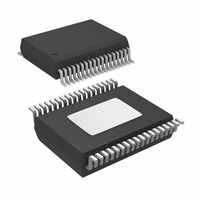


 工商网监
湘ICP备2023018690号
工商网监
湘ICP备2023018690号
