DATA SHEET
www.onsemi.com
Voltage Regulator - Dual,
Low IQ, Low Dropout
MARKING
DIAGRAM
150 mA
NCV8152
XX = Specific Device Code
M = Date Code
The NCV8152 is 150 mA, Dual Output Linear Voltage Regulator.
Device provides a very stable and accurate voltage with ultra low
noise and very high Power Supply Rejection Ratio (PSRR) suitable for
RF applications. The NCV8152 is suitable for powering RF blocks of
automotive infotainment systems and other power sensitive device.
Due to low power consumption the NCV8152 offers high efficiency
and low thermal dissipation.
• Operating Input Voltage Range: 1.9 V to 5.25 V
• Two Independent Output Voltages:
•
OUT1
1
OUT2
2
GND
3
GND
PIN CONNECTIONS
Features
•
•
•
•
•
•
•
•
•
XX M
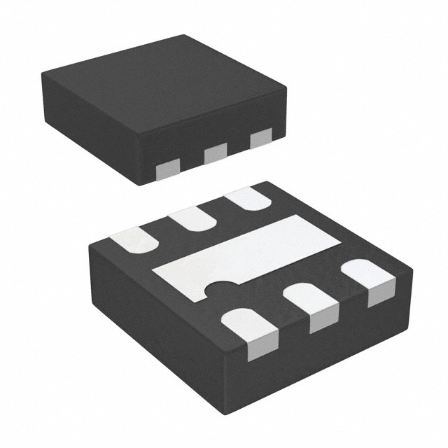
XDFN6, 1.2x1.2
CASE 711AT
6
EN1
5
IN
4
EN2
XDFN6
(Top view)
(for details please refer to the Ordering Information section)
Very Low Dropout: 150 mV Typical at 150 mA
Low IQ of typ. 50 mA per Channel
High PSRR: 75 dB at 1 kHz
Two Independent Enable Pins
Thermal Shutdown and Current Limit Protections
Stable with a 0.22 mF Ceramic Output Capacitor
Available in XDFN6 1.2 x 1.2 mm Package
Active Output Discharge for Fast Output Turn−Off
NCV Prefix for Automotive and Other Applications Requiring
Unique Site and Control Change Requirements; AEC−Q100
Qualified and PPAP Capable; Device Temperature Grade 1: −40°C to
+125°C Ambient Operating Temperature Range
These are Pb−Free Devices
ORDERING INFORMATION
See detailed ordering and shipping information on page 16 of
this data sheet.
Typical Applications
• Wireless LAN, Bluetooth®, ZigBee® Interfaces
• Parking Camera Modules
• Automotive Infotainment Systems
NCV8152
VIN1
VOUT2
IN
EN1
OUT2
EN2
OUT1
VOUT1
GND
CIN1
0.22 mF
COUT1
0.22 mF
COUT2
0.22 mF
Figure 1. Typical Application Schematic
© Semiconductor Components Industries, LLC, 2016
October, 2022 − Rev. 6
1
Publication Order Number:
NCV8152/D
�NCV8152
ENABLE
LOGIC
EN1
THERMAL
SHUTDOWN
MOSFET
DRIVER WITH
CURRENT LIMIT
OUT1
*ACTIVE
DISCHARGE
EN1
GND
EN2
*ACTIVE
DISCHARGE
BANDGAP
REFERENCE
IN
OUT2
MOSFET
DRIVER WITH
CURRENT LIMIT
THERMAL
SHUTDOWN
ENABLE
LOGIC
EN2
Figure 2. Simplified Schematic Block Diagram
PIN FUNCTION DESCRIPTION
Pin No.
XDFN6
Pin
Name
1
OUT1
Regulated output voltage of the first channel. A small 0.22 mF ceramic capacitor is needed from this pin to
ground to assure stability.
2
OUT2
Regulated output voltage of the second channel. A small 0.22 mF ceramic capacitor is needed from this pin
to ground to assure stability.
3
GND
Power supply ground. Soldered to the copper plane allows for effective heat dissipation.
4
EN2
Driving EN2 over 0.9 V turns−on OUT2. Driving EN below 0.4 V turns−off the OUT2 and activates the active
discharge.
5
IN
6
EN1
−
EP
Description
Input pin common for both channels. It is recommended to connect 0.22 mF ceramic capacitor close to the
device pin.
Driving EN1 over 0.9 V turns−on OUT1. Driving EN below 0.4 V turns−off the OUT1 and activates the active
discharge.
Exposed pad must be tied to ground. Soldered to the copper plane allows for effective thermal dissipation.
www.onsemi.com
2
�NCV8152
ABSOLUTE MAXIMUM RATINGS
Rating
Symbol
Value
Unit
VIN
−0.3 V to 6 V
V
Output Voltage
VOUT1,
VOUT2
−0.3 V to VIN + 0.3 V or 6 V
V
Enable Inputs
VEN1,
VEN2
−0.3 V to VIN + 0.3 V or 6 V
V
Input Voltage (Note 1)
Output Short Circuit Duration
tSC
Indefinite
s
Operating Ambient Temperature Range
TA
−40 to +125
°C
TJ(MAX)
150
°C
TSTG
−55 to +150
°C
ESD Capability, Human Body Model (Note 2)
ESDHBM
2000
V
ESD Capability, Machine Model (Note 2)
ESDMM
200
V
Maximum Junction Temperature
Storage Temperature Range
Stresses exceeding those listed in the Maximum Ratings table may damage the device. If any of these limits are exceeded, device functionality
should not be assumed, damage may occur and reliability may be affected.
1. Refer to ELECTRICAL CHARACTERISTICS and APPLICATION INFORMATION for Safe Operating Area.
2. This device series incorporates ESD protection and is tested by the following methods:
ESD Human Body Model tested per EIA/JESD22−A114
ESD Machine Model tested per EIA/JESD22−A115
Latchup Current Maximum Rating tested per JEDEC standard: JESD78.
THERMAL CHARACTERISTICS (Note 3)
Rating
Thermal Characteristics, XDFN6 1.2 x 1.2 mm,
Thermal Resistance, Junction−to−Air
Thermal Characterization Parameter, Junction−to−Lead (Pin 2)
Symbol
Value
qJA
qJL
170
Unit
°C/W
3. Single component mounted on 1 oz, FR4 PCB with 645mm2 Cu area.
RECOMMENDED OPERATING CONDITIONS
Parameter
Symbol
Min
Max
Unit
Input Voltage
VIN
1.9
5.25
V
Junction Temperature
TJ
−40
125
°C
Functional operation above the stresses listed in the Recommended Operating Ranges is not implied. Extended exposure to stresses beyond
the Recommended Operating Ranges limits may affect device reliability.
www.onsemi.com
3
�NCV8152
ELECTRICAL CHARACTERISTIC
−40°C ≤ TJ ≤ 125°C; VIN = VOUT(NOM) + 1 V or 2.5 V, whichever is greater; VEN = 0.9 V, IOUT = 1 mA, CIN = COUT = 0.22 mF. Typical
values are at TJ = +25°C. Min/Max values are specified for TJ = −40°C and TJ = 125°C respectively. (Note 4)
Test Conditions
Parameter
Operating Input Voltage
Output Voltage Accuracy
VOUT > 2 V
−40°C ≤ TJ ≤ 125°C
Symbol
Min
Max
Unit
VIN
1.9
5.25
V
VOUT
−2.8
+2.8
%
−80
+80
mV
VOUT ≤ 2 V
Typ
Line Regulation
VOUT + 0.5 V or 2.5 V ≤ VIN ≤ 5 V
RegLINE
0.02
0.1
%/V
Load Regulation
IOUT = 1 mA to 150 mA
RegLOAD
15
50
mV
VOUT(nom) = 1.8 V
270
420
VOUT(nom) = 3.0 V
150
240
140
240
Dropout Voltage (Note 5)
Iout = 150 mA
VDO
VOUT(nom) = 3.3 V
Output Current Limit
VOUT = 90% VOUT(nom)
ICL
Quiescent Current
IOUT = 0 mA, EN1 = VIN, EN2 = 0 V or EN2 = VIN,
EN1 = 0 V
IQ
50
100
mA
IOUT1 = IOUT2 = 0 mA, VEN1 = VEN2 = VIN
IQ
85
200
mA
IDIS
0.1
1
mA
Shutdown current (Note 6)
VEN ≤ 0.4 V, VIN = 5.25 V
EN Pin Threshold Voltage
High Threshold
Low Threshold
VEN Voltage increasing
VEN Voltage decreasing
EN Pin Input Current
VEN = VIN = 5.25 V
Power Supply Rejection Ratio
VIN = VOUT+1 V for VOUT > 2 V, VIN = 2.5 V,
for VOUT ≤ 2 V, IOUT = 10 mA
Output Noise Voltage
f = 10 Hz to 100 kHz
Active Discharge Resistance
VEN_HI
VEN_LO
150
mV
mA
V
0.9
0.4
IEN
0.3
PSRR
75
dB
VN
75
mVrms
VIN = 4 V, VEN < 0.4 V
RDIS
50
W
Thermal Shutdown Temperature
Temperature increasing from TJ = +25°C
TSD
160
°C
Thermal Shutdown Hysteresis
Temperature falling from TSD
TSDH
f = 1 kHz
−
20
1.0
−
mA
°C
Product parametric performance is indicated in the Electrical Characteristics for the listed test conditions, unless otherwise noted. Product
performance may not be indicated by the Electrical Characteristics if operated under different conditions.
4. Performance guaranteed over the indicated operating temperature range by design and/or characterization. Production tested at TJ = TA
= 25°C. Low duty cycle pulse techniques are used during testing to maintain the junction temperature as close to ambient as possible.
5. Characterized when VOUT falls 100 mV below the regulated voltage at VIN = VOUT(NOM) + 1 V.
6. Shutdown Current is the current flowing into the IN pin when the device is in the disable state.
www.onsemi.com
4
�NCV8152
1.85
2.85
1.84
2.84
VOUT, OUTPUT VOLTAGE (V)
VOUT, OUTPUT VOLTAGE (V)
TYPICAL CHARACTERISTICS
1.83
1.82
1.81
IOUT = 1 mA
1.80
1.79
IOUT = 150 mA
VIN = 2.8 V
VOUT = 1.8 V
CIN = 0.22 mF
COUT = 0.22 mF
1.78
1.77
1.76
1.75
−40 −20
400
350
300
40
60
100
120
140
2.80
IOUT = 150 mA
2.79
VIN = 3.8 V
VOUT = 2.8 V
CIN = 0.22 mF
COUT = 0.22 mF
2.78
2.77
2.76
2.75
−40 −20
0
20
40
60
80
100
120 140
Figure 4. Output Voltage vs. Temperature
VOUT = 2.8 V
750
VIN = 3.8 V
VOUT = 2.8 V
VEN1 = VEN2 = VIN
CIN = 0.22 mF
COUT = 0.22 mF
TJ = 125°C
TJ = 25°C
TJ = −40°C
150
100
0.001
0.01
0.1
1
10
100
1000
675
VEN1 = VEN2 = VIN,
OUT1−LOAD
OUT2−LOAD
600
525
450
VEN1 = VEN2 = VIN,
OUT1−LOAD
375
300
225
VEN1 = 0 V,
VEN2 = VIN,
OUT1−LOAD
150
75
0
0
15
30
45
75
60
90
VIN = 3.8 V
VOUT = 2.8 V
CIN = 0.22 mF
COUT = 0.22 mF
105 120 135 150
IOUT, OUTPUT CURRENT (mA)
IOUT, OUTPUT CURRENT (mA)
Figure 5. Ground Current vs. Output Current −
One Channel Load
Figure 6. Ground Current vs. Output Current −
Different Load Combinations
0.05
125°C
90
80
70
25°C
60
−40°C
50
40
VIN = 3.8 V
VOUT = 2.8 V
CIN = 0.22 mF
COUT = 0.22 mF
30
20
0
IOUT = 1 mA
Figure 3. Output Voltage vs. Temperature
VOUT = 1.8 V
200
10
0
2.81
TJ, JUNCTION TEMPERATURE (°C)
250
50
0
2.82
TJ, JUNCTION TEMPERATURE (°C)
100
IQ, QUIESCENT CURRENT (mA)
80
IGND, GROUND CURRENT (mA)
450
20
REGLINE, LINE REGULATION (%/V)
IGND, GROUND CURRENT (mA)
500
0
2.83
0.5
1.0 1.5 2.0 2.5
3.0 3.5 4.0 4.5 5.0
5.5
0.04
0.03
0.02
0.01
0
−0.01
VIN = 2.5 V to 5.25 V
VOUT = 1.8 V
IOUT = 1 mA
CIN = 0.22 mF
COUT = 0.22 mF
−0.02
−0.03
−0.04
−0.05
−40 −20
0
20
40
60
80
100
120 140
VIN, INPUT VOLTAGE (V)
TJ, JUNCTION TEMPERATURE (°C)
Figure 7. Quiescent Current vs. Input Voltage−
Both Outputs ON
Figure 8. Line Regulation vs. Temperature
VOUT = 1.8 V
www.onsemi.com
5
�NCV8152
TYPICAL CHARACTERISTICS
20
REGLOAD, LOAD REGULATION (mV)
0.04
0.03
0.02
0.01
0
−0.01
VIN = 3.8 V to 5.25 V
VOUT = 2.8 V
IOUT = 1 mA
CIN = 0.22 mF
COUT = 0.22 mF
−0.02
−0.03
−0.04
−0.05
−40 −20
10
0
20
40
60
80
100
120 140
8
7
6
12
10
8
VIN = 2.5 V
VOUT = 1.8 V
IOUT = 1 mA to 150 mA
CIN = 0.22 mF
COUT = 0.22 mF
6
4
2
0
−40 −20
0
20
40
60
80
100
120 140
Figure 10. Load Regulation vs. Temperature
VOUT = 1.8 V
350
4
3
2
1
0
−40 −20
0
20
40
60
80
100
120
140
315
280
245
210
TJ = 125°C
175
TJ = −40°C
140
105
VIN = 2.8 V
VOUT = 1.8 V
CIN = 0.22 mF
COUT = 0.22 mF
70
35
0
TJ = 25°C
0
15
30
45
60
75
90
105 120 135 150
TJ, JUNCTION TEMPERATURE (°C)
IOUT, OUTPUT CURRENT (mA)
Figure 11. Load Regulation vs. Temperature
VOUT = 2.8 V
Figure 12. Dropout Voltage vs. Output Current
VOUT = 1.8 V
350
VDROP, DROPOUT VOLTAGE (mV)
200
VDROP, DROPOUT VOLTAGE (mV)
14
Figure 9. Line Regulation vs. Temperature
VOUT = 2.8 V
5
180
160
140
TJ = 125°C
120
100
TJ = −40°C
80
60
40
20
0
16
TJ, JUNCTION TEMPERATURE (°C)
VIN = 2.5 V
VOUT = 1.8 V
IOUT = 1 mA to 150 mA
CIN = 0.22 mF
COUT = 0.22 mF
9
18
TJ, JUNCTION TEMPERATURE (°C)
VDROP, DROPOUT VOLTAGE (mV)
REGLOAD, LOAD REGULATION (mV)
REGLINE, LINE REGULATION (%/V)
0.05
TJ = 25°C
0
15
30
45
60
75
VIN = 3.8 V
VOUT = 2.8 V
CIN = 0.22 mF
COUT = 0.22 mF
90 105
120 135 150
300
250
VIN = 2.8 V
VOUT = 1.8 V
CIN = 0.22 mF
COUT = 0.22 mF
IOUT = 150 mA
200
IOUT = 75 mA
150
100
IOUT = 0 mA
50
0
−40 −20
0
20
40
60
80
100
120 140
IOUT, OUTPUT CURRENT (mA)
TJ, JUNCTION TEMPERATURE (°C)
Figure 13. Dropout Voltage vs. Output Current
VOUT = 2.8 V
Figure 14. Dropout Voltage vs. Temperature
VOUT = 1.8 V
www.onsemi.com
6
�NCV8152
TYPICAL CHARACTERISTICS
175
VDROP, DROPOUT VOLTAGE (mV)
200
600
VIN = 3.8 V
VOUT = 2.8 V
CIN = 0.22 mF
COUT = 0.22 mF
IOUT = 150 mA
150
125
IOUT = 75 mA
100
75
50
IOUT = 0 mA
25
0
−40 −20
0
20
40
60
80
100
500
400
300
200
100
0
120 140
0.9 1.2
1.5
1.8
2.1
2.4
2.7
3.0
3.3 3.6
TJ, JUNCTION TEMPERATURE (°C)
VOUT, OUTPUT VOLTAGE (V)
Figure 15. Dropout Voltage vs. Temperature
VOUT = 2.8 V
Figure 16. Dropout Voltage vs. Output Voltage
ISC, SHORT−CIRCUIT CURRENT (mA)
400
360
320
280
240
200
160
VIN = 3.8 V
VOUT = 0 V
CIN = 0.22 mF
COUT = 0.22 mF
120
80
40
0
−40 −20
0
20
40
60
80
100
300
270
240
210
180
150
120
90
60
0
2.4
2.8
3.2
3.6
4.0
4.4
4.8
5.2
5.6
TJ, JUNCTION TEMPERATURE (°C)
VIN, INPUT VOLTAGE (V)
Figure 17. Short−Circuit Current vs.
Temperature
Figure 18. Short−Circuit Current vs. Input
Voltage
200
1.0
180
0.9
160
140
120
100
80
VIN = 5.5 V
VOUT = 2.8 V
CIN = 0.22 mF
COUT = 0.22 mF
60
40
20
0
−40 −20
VOUT = 0 V
CIN = 0.22 mF
COUT = 0.22 mF
30
120 140
0
20
40
60
80
100
VEN, ENABLE VOLTAGE (V)
IDIS, DISABLE CURRENT (nA)
ISC, SHORT−CIRCUIT CURRENT (mA)
VDROP, DROPOUT VOLTAGE (mV)
225
0.8
0.7
OFF −> ON
0.6
ON −> OFF
0.5
0.4
0.3
VIN = 3.8 V
VOUT = 2.8 V
CIN = 0.22 mF
COUT = 0.22 mF
0.2
0.1
0
−40 −20
120 140
0
20
40
60
80
100
120 140
TJ, JUNCTION TEMPERATURE (°C)
TJ, JUNCTION TEMPERATURE (°C)
Figure 19. Disable Current vs. Temperature
Figure 20. Enable Voltage Threshold vs.
Temperature
www.onsemi.com
7
6.0
�NCV8152
TYPICAL CHARACTERISTICS
50
RDIS, DISCHARGE RESISTIVITY (W)
500
400
350
300
250
200
VIN = 3.8 V
VOUT = 2.8 V
CIN = 0.22 mF
COUT = 0.22 mF
150
100
50
0
−40 −20
0
20
40
60
80
140
RR, RIPPLE REJECTION (dB)
50
40
0
0.1
VIN = 2.5 V
VOUT = 1.2 V
CIN = none
COUT = 0.22 mF
1
10
100
5
0
−40 −20
0
20
40
60
80
100
120 140
1000
80
70
60
50
40
30
IOUT = 1 mA
IOUT = 10 mA
IOUT = 100 mA
IOUT = 150 mA
20
10
0
0.1
10000
VIN = 2.5 V
VOUT = 1.2 V
CIN = none
COUT = 1 mF
90
1
10
100
1000
10000
FREQUENCY (kHz)
100
IOUT = 1 mA
IOUT = 10 mA
IOUT = 100 mA
IOUT = 150 mA
70
60
50
40
0
0.1
10
Figure 24. Power Supply Rejection Ratio,
VOUT = 1.2 V, COUT = 1 mF
80
10
VIN = 3.8 V
VOUT = 2.8 V
CIN = 0.22 mF
COUT = 0.22 mF
15
FREQUENCY (kHz)
90
20
20
Figure 23. Power Supply Rejection Ratio,
VOUT = 1.2 V, COUT = 0.22 mF
100
30
25
100
IOUT = 1 mA
IOUT = 10 mA
IOUT = 100 mA
IOUT = 150 mA
60
10
30
TJ, JUNCTION TEMPERATURE (°C)
70
20
35
Figure 22. Discharge Resistance vs.
Temperature
80
30
40
TJ, JUNCTION TEMPERATURE (°C)
90
RR, RIPPLE REJECTION (dB)
120
45
Figure 21. Current to Enable Pin vs.
Temperature
100
RR, RIPPLE REJECTION (dB)
100
RR, RIPPLE REJECTION (dB)
IEN, ENABLE CURRENT (nA)
450
VIN = 3.8 V
VOUT = 2.8 V
CIN = none
COUT = 0.22 mF
1
10
100
1000
10000
VIN = 3.8 V
VOUT = 2.8 V
CIN = none
COUT = 1 mF
90
80
70
60
50
40
30
20
10
0
0.1
IOUT = 1 mA
IOUT = 10 mA
IOUT = 100 mA
IOUT = 150 mA
1
10
100
1000
10000
FREQUENCY (kHz)
FREQUENCY (kHz)
Figure 25. Power Supply Rejection Ratio,
VOUT = 2.8 V, COUT = 0.22 mF
Figure 26. Power Supply Rejection Ratio,
VOUT = 2.8 V, COUT = 1 mF
www.onsemi.com
8
�OUTPUT VOLTAGE NOISE (mV/rtHz)
NCV8152
10
1
IOUT = 150 mA
IOUT
0.1
0.01
1 mA
VIN = 2.8 V
VOUT = 1.8 V
CIN = 0.22 mF
COUT = 0.22 mF
MLCC, X7R,
1206 size
0.001
0.01
0.1
IOUT = 10 mA
RMS Output Noise (mV)
10 Hz − 100 kHz
100 Hz − 100 kHz
68.07
67.07
10 mA
67.30
66.31
150 mA
69.74
68.80
IOUT = 1 mA
1
100
10
1000
FREQUENCY (kHz)
Figure 27. Output Voltage Noise Spectral Density for VOUT = 1.8 V, COUT = 220 nF
OUTPUT VOLTAGE NOISE (mV/rtHz)
10
IOUT = 150 mA
1
IOUT
0.1
0.01
VIN = 2.8 V
VOUT = 1.8 V
CIN = 1 mF
COUT = 1 mF
MLCC, X7R,
1206 size
0.001
0.01
0.1
RMS Output Noise (mV)
10 Hz − 100 kHz
100 Hz − 100 kHz
75.33
1 mA
76.23
10 mA
67.12
66.12
150 mA
69.06
68.12
IOUT = 10 mA
IOUT = 1 mA
1
10
100
1000
FREQUENCY (kHz)
Figure 28. Output Voltage Noise Spectral Density for VOUT = 1.8 V, COUT = 1 mF
OUTPUT VOLTAGE NOISE (mV/rtHz)
10
1
IOUT = 150 mA
IOUT
0.1
0.01
VIN = 3.8 V
VOUT = 2.8 V
CIN = 0.22 mF
COUT = 0.22 mF
MLCC, X7R,
1206 size
0.001
0.01
0.1
IOUT = 10 mA
RMS Output Noise (mV)
10 Hz − 100 kHz
100 Hz − 100 kHz
1 mA
93.42
91.99
10 mA
92.88
91.45
150 mA
94.67
93.26
IOUT = 1 mA
1
10
100
1000
FREQUENCY (kHz)
Figure 29. Output Voltage Noise Spectral Density for VOUT = 2.8 V, COUT = 220 nF
www.onsemi.com
9
�NCV8152
IOUT = 150 mA
1
IOUT
0.1
0.01
VIN = 3.8 V
VOUT = 2.8 V
CIN = 1 mF
COUT = 1 mF
MLCC, X7R,
1206 size
0.001
0.01
0.1
RMS Output Noise (mV)
10 Hz − 100 kHz
100 Hz − 100 kHz
100.86
1 mA
102.14
10 mA
93.03
91.59
150 mA
94.74
93.12
IOUT = 10 mA
IOUT = 1 mA
1
10
100
1000
FREQUENCY (kHz)
Figure 30. Output Voltage Noise Spectral Density for VOUT = 2.8 V, COUT = 1 mF
100
VOUT = 2.8 V
10
ESR (W)
OUTPUT VOLTAGE NOISE (mV/rtHz)
10
1
UNSTABLE OPERATION
VOUT = 1.8 V
STABLE OPERATION
0.1
0.01
0
15
30
45
60
75
90
105 120 135
IOUT, OUTPUT CURRENT (mA)
Figure 31. Output Capacitor ESR vs. Output
Current
www.onsemi.com
10
150
�NCV8152
VIN = 3.8 V
VOUT1 = disable
VOUT2 = 1.2 V
IOUT1 = 10 mA
COUT1 = COUT2 = 220 nF
40 ms/div
VOUT1
VOUT2
40 ms/div
500 mV/div
Figure 33. Enable Turn−on Response −
VR1 = 10 mA, VR2 = 10 mA
50 mA/div
IIN
VOUT2
VIN = 3.8 V
VOUT1 = disable
VOUT2 = 1.2 V
IOUT2 = 150 mA
COUT1 = COUT2 = 220 nF
VOUT1
VOUT2
VIN = 3.8 V
VOUT1 = 2.8 V
VOUT2 = 1.2 V
IOUT1 = 10 mA
IOUT2 = 150 mA
COUT1 = COUT2 = 220 nF
40 ms/div
Figure 35. Enable Turn−on Response −
VR1 = 10 mA, VR2 = 150 mA
tRISE = 1 ms
VOUT2
VIN = 3.8 V to 4.8 V
IOUT2 = 10 mA
COUT1 = 220 nF
COUT2 = 220 nF
VIN
tFALL = 1 ms
VOUT1
20 mV/div
VIN
500 mV/div
40 ms/div
Figure 34. Enable Turn−on Response −
VR1 = Off, VR2 = 150 mA
VOUT1
20 mV/div
1 V/div 1 V/div
VOUT1
20 mV/div
500 mV/div
1 V/div
1 V/div
IIN
VEN
20 mV/div
500 mV/div
Figure 32. Enable Turn−on Response −
VR1 = Off, VR2 = 10 mA
VEN
VIN = 3.8 V
VOUT1 = 2.8 V
VOUT2 = 1.2 V
IOUT1 = 10 mA
IOUT2 = 10 mA
COUT1 = COUT2 = 220 nF
50 mA/div
VOUT2
1 V/div
VOUT1
IIN
1 V/div
1 V/div
1 V/div
IIN
VEN
50 mA/div
500 mV/div
VEN
50 mA/div
500 mV/div
TYPICAL CHARACTERISTICS
VOUT2
VIN = 4.8 V to 3.8 V
IOUT2 = 150 mA
COUT1 = 220 nF
COUT2 = 220 nF
2 ms/div
2 ms/div
Figure 36. Line Transient Response − Rising
Edge, VEN1 = 0 V, VEN2 = VIN, VOUT2 = 3.3 V,
IOUT2 = 10 mA
Figure 37. Line Transient Response − Falling
Edge, VEN1 = 0 V, VEN2 = VIN, VOUT2 = 3.3 V,
IOUT2 = 10 mA
www.onsemi.com
11
�NCV8152
VIN = 3.8 V to 4.8 V
IOUT2 = 10 mA
COUT1 = 220 nF
COUT2 = 220 nF
VOUT2
VOUT1
tFALL = 1 ms
VIN = 4.8 V to 3.8 V
IOUT2 = 150 mA
COUT1 = 220 nF
COUT2 = 220 nF
VOUT2
2 ms/div
Figure 39. Line Transient Response − Falling
Edge, VEN1 = 0 V, VEN2 = VIN, VOUT2 = 3.3 V,
IOUT2 = 150 mA
IOUT2
50 mA/div
2 ms/div
Figure 38. Line Transient Response − Rising
Edge, VEN1 = 0 V, VEN2 = VIN, VOUT2 = 3.3 V,
IOUT2 = 150 mA
tRISE = 1 ms
VOUT2
20 mV/div 50 mA/div
20 mV/div 50 mA/div
50 mA/div
20 mV/div
VOUT1
VIN
20 mV/div
500 mV/div
tRISE = 1 ms
20 mV/div
VIN
20 mV/div
500 mV/div
TYPICAL CHARACTERISTICS
VIN = 3.8 V
VOUT1 = 2.8 V
VOUT2 = 1.2 V
IOUT1 = 10 mA
COUT1 = 220 nF
COUT2 = 220 nF
VOUT1
IOUT2
tFALL = 1 ms
VOUT2
VIN = 3.8 V
VOUT1 = 2.8 V
VOUT2 = 1.2 V
IOUT1 = 10 mA
COUT1 = 220 nF
COUT2 = 220 nF
VOUT1
2 ms/div
10 ms/div
Figure 40. Load Transient Response − Rising
Edge, IOUT = 1 mA to 150 mA
Figure 41. Load Transient Response − Falling
Edge, IOUT = 150 mA to 1 mA
50 mA/div
IOUT2
tRISE = 500 ns
VOUT2
20 mV/div 100 mV/div
20 mV/div 100 mV/div
50 mA/div
IOUT2
VIN = 3.8 V
VOUT1 = 2.8 V
VOUT2 = 1.2 V
IOUT1 = 10 mA
COUT1 = 220 nF
COUT2 = 220 nF
VOUT1
tFALL = 500 ns
VOUT2
VIN = 3.8 V
VOUT1 = 2.8 V
VOUT2 = 1.2 V
IOUT1 = 10 mA
COUT1 = 220 nF
COUT2 = 220 nF
VOUT1
2 ms/div
10 ms/div
Figure 42. Load Transient Response − Rising
Edge, IOUT = 0.1 mA to 150 mA
Figure 43. Load Transient Response − Falling
Edge, IOUT = 150 mA to 0.1 mA
www.onsemi.com
12
�NCV8152
50 mA/div
tRISE = 500 ns
VOUT2
VIN = 3.8 V
VOUT1 = 2.8 V
VOUT2 = 1.2 V
IOUT1 = 10 mA
COUT1 = 220 nF
COUT2 = 220 nF
VOUT1
tFALL = 500 ns
50 mV/div
IOUT2
IOUT2
VIN = 3.8 V
VOUT1 = 2.8 V
VOUT2 = 1.2 V
IOUT1 = 10 mA
COUT1 = 220 nF
COUT2 = 220 nF
VOUT2
VOUT1
20 mV/div
20 mV/div
50 mV/div
50 mA/div
TYPICAL CHARACTERISTICS
2 ms/div
2 ms/div
Figure 44. Load Transient Response − Rising
Edge, IOUT = 50 mA to 150 mA
Figure 45. Load Transient Response − Falling
Edge, IOUT = 150 mA to 50 mA
VOUT2
50 mA/div
50 mV/div
VOUT1
tRISE = 500 ns
VIN = 4.3 V
VOUT1 = 3.3 V
VOUT2 = 3.0 V
IOUT1 = 10 mA
COUT1 = 220 nF
COUT2 = 220 nF
20 mV/div
50 mV/div
IOUT1
20 mV/div
50 mA/div
IOUT1
2 ms/div
VIN = 4.3 V
VOUT1 = 3.3 V
VOUT2 = 3.0 V
IOUT1 = 10 mA
COUT1 = 220 nF
COUT2 = 220 nF
VOUT2
10 ms/div
Figure 48. Load Transient Response − Falling
Edge, IOUT = 150 mA to 1 mA
tRISE = 1 ms
VOUT1
VIN = 4.3 V
VOUT1 = 3.3 V
VOUT2 = 3.0 V
IOUT1 = 10 mA
COUT1 = 220 nF
COUT2 = 220 nF
VOUT2
IOUT1
50 mA/div
IOUT1
VOUT1
tFALL = 1 ms
20 mV/div 100 mV/div
20 mV/div 100 mV/div
50 mA/div
Figure 47. Load Transient Response − Rising
Edge, IOUT = 1 mA to 150 mA
tFALL = 500 ns
VOUT1
VIN = 4.3 V
VOUT1 = 3.3 V
VOUT2 = 3.0 V
IOUT1 = 10 mA
COUT1 = 220 nF
COUT2 = 220 nF
VOUT2
2 ms/div
20 ms/div
Figure 46. Load Transient Response − Rising
Edge, IOUT = 0.1 mA to 150 mA
Figure 49. Load Transient Response − Falling
Edge, IOUT = 150 mA to 0.1 mA
www.onsemi.com
13
�NCV8152
50 mA/div
VOUT1
VIN = 4.3 V
VOUT1 = 3.3 V
VOUT2 = 3.0 V
IOUT1 = 10 mA
COUT1 = 220 nF
COUT2 = 220 nF
VOUT2
VOUT1
VOUT2
VIN = 4.3 V
VOUT1 = 3.3 V
VOUT2 = 3.0 V
IOUT1 = 10 mA
COUT1 = 220 nF
COUT2 = 220 nF
2 ms/div
2 ms/div
Figure 50. Load Transient Response − Rising
Edge, IOUT = 50 mA to 150 mA
Figure 51. Load Transient Response − Falling
Edge, IOUT = 150 mA to 50 mA
VIN = 4.3 V
VOUT1 = 2.8 V
IOUT1 = 10 mA
IOUT2 = 10 mA
CIN = COUT1 =
COUT1 = 220 nF
VIN
VOUT1
Full Load
Overheating
IOUT1
VOUT1
500 mV/div
VOUT2
VIN = 5.5 V
VOUT1 = 1.2 V
VOUT2 = 3.0 V
CIN = COUT1 =
COUT1 = 220 nF
Thermal Shutdown TSD Cycling
10 ms/div
Figure 52. Turn−on/off − Slow Rising VIN
Figure 53. Short−Circuit and Thermal
Shutdown
500 mV/div
20 ms/div
1 V/div
1 V/div
tFALL = 1 ms
50 mV/div
tRISE = 1 ms
IOUT1
20 mV/div
IOUT1
50 mA/div
20 mV/div 50 mV/div
50 mA/div
TYPICAL CHARACTERISTICS
VEN
VIN = 3.8 V
VOUT1 = 2.8 V
VOUT2 = 1.2 V
tFALL = 1 ms
VOUT1
COUT = 4.7 mF
COUT = 1 mF
COUT = 220 nF
100 ms/div
Figure 54. Enable Turn−off
www.onsemi.com
14
�NCV8152
APPLICATIONS INFORMATION
General
disable state the device consumes as low as typ. 10 nA from
the VIN.
If the EN pin voltage >0.9 V the device is guaranteed to
be enabled. The NCV8152 regulates the output voltage and
the active discharge transistor is turned−off.
The both EN pin has internal pull−down current source
with typ. value of 300 nA which assures that the device is
turned−off when the EN pin is not connected. In the case
where the EN function isn’t required the EN should be tied
directly to IN.
The NCV8152 is a dual output high performance 150 mA
Low Dropout Linear Regulator. This device delivers very
high PSRR (75 dB at 1 kHz) and excellent dynamic
performance as load/line transients. In connection with low
quiescent current this device is very suitable for various
battery powered applications such as tablets, cellular
phones, wireless and many others. Each output is fully
protected in case of output overload, output short circuit
condition and overheating, assuring a very robust design.
The NCV8152 device is housed in XDFN−6 1.2 mm x
1.2 mm package which is useful for space constrains
application.
Output Current Limit
Output Current is internally limited within the IC to a
typical 280 mA. The NCV8152 will source this amount of
current measured with a voltage drops on the 90% of the
nominal VOUT. If the Output Voltage is directly shorted to
ground (VOUT = 0 V), the short circuit protection will limit
the output current to 300 mA (typ). The current limit and
short circuit protection will work properly over whole
temperature range and also input voltage range. There is no
limitation for the short circuit duration. This protection
works separately for each channel. Short circuit on the one
channel do not influence second channel which will work
according to specification.
Input Capacitor Selection (CIN)
It is recommended to connect at least a 0.22 mF Ceramic
X5R or X7R capacitor as close as possible to the IN pin of
the device. This capacitor will provide a low impedance path
for unwanted AC signals or noise modulated onto constant
input voltage. There is no requirement for the min. or max.
ESR of the input capacitor but it is recommended to use
ceramic capacitors for their low ESR and ESL. A good input
capacitor will limit the influence of input trace inductance
and source resistance during sudden load current changes.
Larger input capacitor may be necessary if fast and large
load transients are encountered in the application.
Thermal Shutdown
When the die temperature exceeds the Thermal Shutdown
threshold (TSD − 160°C typical), Thermal Shutdown event
is detected and the affected channel is turn−off. Second
channel still working. The channel which is overheated will
remain in this state until the die temperature decreases below
the Thermal Shutdown Reset threshold (TSDU − 140°C
typical). Once the device temperature falls below the 140°C
the appropriate channel is enabled again. The thermal
shutdown feature provides the protection from a
catastrophic device failure due to accidental overheating.
This protection is not intended to be used as a substitute for
proper heat sinking. The long duration of the short circuit
condition to some output channel could cause turn−off other
output when heat sinking is not enough and temperature of
the other output reach TSD temperature.
Output Decoupling (COUT)
The NCV8152 requires an output capacitor for each
output connected as close as possible to the output pin of the
regulator. The recommended capacitor value is 0.22 mF and
X7R or X5R dielectric due to its low capacitance variations
over the specified temperature range. The NCV8152 is
designed to remain stable with minimum effective
capacitance of 0.15 mF to account for changes with
temperature, DC bias and package size. Especially for small
package size capacitors such as 0201 the effective
capacitance drops rapidly with the applied DC bias.
There is no requirement for the minimum value of
Equivalent Series Resistance (ESR) for the COUT but the
maximum value of ESR should be less than 2 W. Larger
output capacitors and lower ESR could improve the load
transient response or high frequency PSRR. It is not
recommended to use tantalum capacitors on the output due
to their large ESR. The equivalent series resistance of
tantalum capacitors is also strongly dependent on the
temperature, increasing at low temperature.
Power Dissipation
As power dissipated in the NCV8152 increases, it might
become necessary to provide some thermal relief. The
maximum power dissipation supported by the device is
dependent upon board design and layout. Mounting pad
configuration on the PCB, the board material, and the
ambient temperature affect the rate of junction temperature
rise for the part. For reliable operation, junction temperature
should be limited to +125°C.
The maximum power dissipation the NCV8152 can
handle is given by:
Enable Operation
The NCV8152 uses the dedicated EN pin for each output
channel. This feature allows driving outputs separately.
If the EN pin voltage is VIN.
Due to this fact in cases, where the extended reverse current
condition can be anticipated the device may require
additional external protection.
PCB Layout Recommendations
To obtain good transient performance and good regulation
characteristics place input and output capacitors close to the
device pins and make the PCB traces wide. In order to
minimize the solution size, use 0402 capacitors. Larger
copper area connected to the pins will also improve the
device thermal resistance. The actual power dissipation can
be calculated from the equation above (Equation 2). Expose
pad should be tied the shortest path to the GND pin.
Power Supply Rejection Ratio
The NCV8152 features very good Power Supply
Rejection ratio. If desired the PSRR at higher frequencies in
the range 100 kHz − 10 MHz can be tuned by the selection
of COUT capacitor and proper PCB layout.
Turn−On Time
The turn−on time is defined as the time period from EN
assertion to the point in which VOUT will reach 98% of its
ORDERING INFORMATION
Voltage Option
(OUT1/OUT2)
Marking
Marking
Rotation
NCV8152MX180150TCG
1.8 V/1.5 V
AN
0°
NCV8152MX180180TCG (Note 7)
1.8 V/1.8 V
AJ
0°
NCV8152MX180280TCG (Note 7)
1.8 V/2.8 V
5
180°
NCV8152MX280180TCG (Note 7)
2.8 V/1.8 V
6
270°
NCV8152MX300180TCG (Note 7)
3.0 V/1.8 V
L
90°
NCV8152MX330180TCG (Note 7)
3.3 V/1.8 V
R
90°
Device
Package
Shipping†
XDFN-6
(Pb-Free)
3000 or 5000 /
Tape & Reel
(Note 7)
†For information on tape and reel specifications, including part orientation and tape sizes, please refer to our Tape and Reel Packaging
Specifications Brochure, BRD8011/D.
7. Product processed after October 1, 2022 are shipped with quantity 5000 units / tape & reel.
ZigBee is a registered trademark of ZigBee Alliance.
Bluetooth is a registered trademark of Bluetooth SIG.
www.onsemi.com
16
�MECHANICAL CASE OUTLINE
PACKAGE DIMENSIONS
XDFN6 1.20x1.20, 0.40P
CASE 711AT
ISSUE C
SCALE 4:1
D
PIN ONE
REFERENCE
DATE 04 DEC 2015
NOTES:
1. DIMENSIONING AND TOLERANCING PER
ASME Y14.5M, 1994.
2. CONTROLLING DIMENSION: MILLIMETERS.
3. DIMENSION b APPLIES TO THE PLATED
TERMINALS.
4. COPLANARITY APPLIES TO THE PAD AS
WELL AS THE TERMINALS.
A
B
ÍÍÍ
ÍÍÍ
ÍÍÍ
E
L
TOP VIEW
DETAIL A
OPTIONAL
CONSTRUCTION
A
0.05 C
DIM
A
A1
b
D
D2
E
E2
e
L
L1
A1
GENERIC
MARKING DIAGRAM*
0.05 C
C
SIDE VIEW
NOTE 4
MILLIMETERS
TYP
MAX
0.37
0.45
0.03
0.05
0.18
0.23
1.20
1.25
0.94
1.04
1.20
1.25
0.40
0.30
0.40 BSC
0.15
0.20
0.25
0.05
0.00
0.10
MIN
0.30
0.00
0.13
1.15
0.84
1.15
0.20
SEATING
PLANE
XX M
D2
1
3
6X
L1
XX = Specific Device Code
M = Date Code
E2
6X
*This information is generic. Please refer
to device data sheet for actual part marking. Pb−Free indicator, “G” or microdot “
G”, may or may not be present.
L
6
DETAIL A
4
6X
e
b
0.10
BOTTOM VIEW
M
C A B
NOTE 3
RECOMMENDED
MOUNTING FOOTPRINT*
1.08
PACKAGE
OUTLINE
6X
0.37
1.40
0.40
1
0.40
PITCH
6X
0.24
DIMENSIONS: MILLIMETERS
*For additional information on our Pb−Free strategy and soldering
details, please download the ON Semiconductor Soldering and
Mounting Techniques Reference Manual, SOLDERRM/D.
DOCUMENT NUMBER:
DESCRIPTION:
98AON76141F
XDFN6, 1.20 X 1.20, 0.40P
Electronic versions are uncontrolled except when accessed directly from the Document Repository.
Printed versions are uncontrolled except when stamped “CONTROLLED COPY” in red.
PAGE 1 OF 1
ON Semiconductor and
are trademarks of Semiconductor Components Industries, LLC dba ON Semiconductor or its subsidiaries in the United States and/or other countries.
ON Semiconductor reserves the right to make changes without further notice to any products herein. ON Semiconductor makes no warranty, representation or guarantee regarding
the suitability of its products for any particular purpose, nor does ON Semiconductor assume any liability arising out of the application or use of any product or circuit, and specifically
disclaims any and all liability, including without limitation special, consequential or incidental damages. ON Semiconductor does not convey any license under its patent rights nor the
rights of others.
© Semiconductor Components Industries, LLC, 2019
www.onsemi.com
�onsemi,
, and other names, marks, and brands are registered and/or common law trademarks of Semiconductor Components Industries, LLC dba “onsemi” or its affiliates
and/or subsidiaries in the United States and/or other countries. onsemi owns the rights to a number of patents, trademarks, copyrights, trade secrets, and other intellectual property.
A listing of onsemi’s product/patent coverage may be accessed at www.onsemi.com/site/pdf/Patent−Marking.pdf. onsemi reserves the right to make changes at any time to any
products or information herein, without notice. The information herein is provided “as−is” and onsemi makes no warranty, representation or guarantee regarding the accuracy of the
information, product features, availability, functionality, or suitability of its products for any particular purpose, nor does onsemi assume any liability arising out of the application or use
of any product or circuit, and specifically disclaims any and all liability, including without limitation special, consequential or incidental damages. Buyer is responsible for its products
and applications using onsemi products, including compliance with all laws, regulations and safety requirements or standards, regardless of any support or applications information
provided by onsemi. “Typical” parameters which may be provided in onsemi data sheets and/or specifications can and do vary in different applications and actual performance may
vary over time. All operating parameters, including “Typicals” must be validated for each customer application by customer’s technical experts. onsemi does not convey any license
under any of its intellectual property rights nor the rights of others. onsemi products are not designed, intended, or authorized for use as a critical component in life support systems
or any FDA Class 3 medical devices or medical devices with a same or similar classification in a foreign jurisdiction or any devices intended for implantation in the human body. Should
Buyer purchase or use onsemi products for any such unintended or unauthorized application, Buyer shall indemnify and hold onsemi and its officers, employees, subsidiaries, affiliates,
and distributors harmless against all claims, costs, damages, and expenses, and reasonable attorney fees arising out of, directly or indirectly, any claim of personal injury or death
associated with such unintended or unauthorized use, even if such claim alleges that onsemi was negligent regarding the design or manufacture of the part. onsemi is an Equal
Opportunity/Affirmative Action Employer. This literature is subject to all applicable copyright laws and is not for resale in any manner.
PUBLICATION ORDERING INFORMATION
LITERATURE FULFILLMENT:
Email Requests to: orderlit@onsemi.com
onsemi Website: www.onsemi.com
◊
TECHNICAL SUPPORT
North American Technical Support:
Voice Mail: 1 800−282−9855 Toll Free USA/Canada
Phone: 011 421 33 790 2910
Europe, Middle East and Africa Technical Support:
Phone: 00421 33 790 2910
For additional information, please contact your local Sales Representative
�


 工商网监
湘ICP备2023018690号
工商网监
湘ICP备2023018690号
