DATA SHEET
www.onsemi.com
LDO Regulator Ultra‐Low IQ, CMOS
6
1
150 mA
NCV8170
The NCV8170 series of CMOS low dropout regulators are designed
specifically for continuous on battery-powered applications which
require ultra-low quiescent current. The ultra-low consumption of typ.
500 nA ensures long battery life and dynamic transient boost feature
improves device transient response for wireless communication
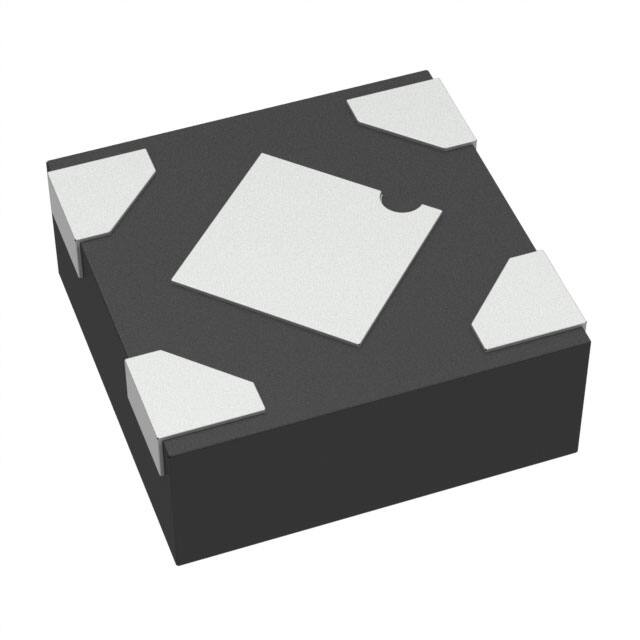
applications. The device is available in small 1 × 1 mm xDFN4 and
SOT−563 packages.
Features
•
•
•
•
•
•
•
•
•
•
•
•
1
SOT−563
XV SUFFIX
CASE 463A
XDFN4
MX SUFFIX
CASE 711AJ
Operating Input Voltage Range: 2.2 V to 5.5 V
Output Voltage Range: 1.2 V to 3.6 V (0.1 V Steps)
Ultra-Low Quiescent Current Typ. 0.5 mA
Low Dropout: 170 mV Typ. at 150 mA
High Output Voltage Accuracy ±1%
Stable with Ceramic Capacitors 1 mF
Over-Current Protection
Thermal Shutdown Protection
NCV8170A for Active Discharge Option
Available in Small 1 × 1 mm xDFN4 and SOT−563 Packages
NCV Prefix for Automotive and Other Applications Requiring
Unique Site and Control Change Requirements; AEC−Q100
Qualified and PPAP Capable
These Devices are Pb−Free, Halogen Free/BFR Free and are RoHS
Compliant
MARKING DIAGRAMS
XDFN4
XX M
1
XX = Specific Device Code
M = Date Code
SOT−563
XX MG
1
XX = Specific Device Code
M = Month Code
G
= Pb−Free Package
ORDERING INFORMATION
See detailed ordering, marking and shipping information on
page 19 of this data sheet.
Typical Applications
•
•
•
•
Telematics and Infotainment Systems
Automotive Keyless Entry Systems
ADAS Camera Modules
Navigation Systems
VIN
CIN
IN
1 mF
NCV8170
VOUT
OUT
COUT
EN
1 mF
GND
Figure 1. Typical Application Schematic
© Semiconductor Components Industries, LLC, 2015
September, 2022 − Rev. 7
1
Publication Order Number:
NCV8170/D
�NCV8170
PIN FUNCTION DESCRIPTION
Pin No.
XDFN4
Pin No.
SOT−563
Pin Name
4
1
IN
2
2
GND
3
6
EN
1
3
OUT
Output Pin
EPAD
Internally Connected to GND
EPAD
Description
Power Supply Input Voltage
Power Supply Ground
Chip Enable Pin (Active “H”)
4
NC
No Connect
5
GND
Power Supply Ground
ABSOLUTE MAXIMUM RATINGS
Symbol
VIN
Rating
Input Voltage (Note 1)
VOUT
Output Voltage
VCE
Chip Enable Input
TJ(MAX)
TSTG
Maximum Junction Temperature
Storage Temperature
Value
Unit
6.0
V
−0.3 to VIN + 0.3
V
−0.3 to 6.0
V
125
°C
−55 to 150
°C
ESDHBM
ESD Capability, Human Body Model (Note 2)
2000
V
ESDMM
ESD Capability, Machine Model (Note 2)
200
V
Stresses exceeding those listed in the Maximum Ratings table may damage the device. If any of these limits are exceeded, device functionality
should not be assumed, damage may occur and reliability may be affected.
1. Refer to ELECTRICAL CHARACTERISTICS and APPLICATION INFORMATION for Safe Operating Area.
2. This device series incorporates ESD protection and is tested by the following methods:
ESD Human Body Model tested per AEC-Q100-002 (EIA/JESD22-A114)
ESD Machine Model tested per AEC-Q100-003 (EIA/JESD22-A115)
Latchup Current Maximum Rating tested per JEDEC standard: JESD78
THERMAL CHARACTERISTICS
Symbol
RqJA
Rating
Value
Thermal Characteristics, Thermal Resistance, Junction-to-Air
XDFN4 1 × 1 mm
SOT−563
Figure 2. Simplified Block Diagram
www.onsemi.com
2
250
200
Unit
°C/W
�NCV8170
ELECTRICAL CHARACTERISTICS − VOLTAGE VERSION 1.2 V
(−40°C ≤ TJ ≤ 125°C; VIN = 2.5 V; IOUT = 1 mA, CIN = COUT = 1.0 mF, unless otherwise noted. Typical values are at TA = +25°C.) (Note 3)
Symbol
VIN
VOUT
Parameter
Test Conditions
Min
Typ
Max
Unit
2.2
−
5.5
V
TA = +25°C
1.188
1.2
1.212
V
−40°C ≤ TJ ≤ 125°C
1.176
1.2
1.224
Operating Input Voltage
Output Voltage
LineReg
Line Regulation
2.5 V < VIN ≤ 5.5 V, IOUT = 1 mA
LoadReg
Load Regulation
0 mA < IOUT ≤ 150 mA, VIN = 2.5 V
−
0.05
0.20
%/V
−20
1
20
mV
VDO
Dropout Voltage
(Note 4)
−
−
−
mV
IOUT
Output Current
(Note 5)
150
−
−
mA
ISC
Short Circuit Current Limit
VOUT = 0 V
−
225
−
mA
IQ
Quiescent Current
IOUT = 0 mA
−
0.5
0.9
mA
ISTB
Standby Current
VEN = 0 V, TJ = 25°C
−
0.1
0.5
mA
VENH
EN Pin Threshold Voltage
EN Input Voltage “H”
1.2
−
−
V
VENL
EN Pin Threshold Voltage
EN Input Voltage “L”
−
−
0.4
V
EN Pin Current
VEN ≤ VIN ≤ 5.5 V (Note 6)
−
10
−
nA
PSRR
Power Supply Rejection Ratio
f = 1 kHz, VIN = 2.2 V + 200 mVpp Modulation
IOUT = 150 mA
IOUT = 10 mA
−
−
57
63
−
−
VNOISE
Output Noise Voltage
VIN = 5.5 V, IOUT = 1 mA,
f = 100 Hz to 1 MHz, COUT = 1 mF
−
85
−
mVrms
Active Output Discharge
Resistance (A option only)
VIN = 5.5 V, VEN = 0 V (Note 6)
−
100
−
W
TSD
Thermal Shutdown Temperature
Temperature Increasing from TJ = +25°C
(Note 6)
−
175
−
°C
TSDH
Thermal Shutdown Hysteresis
Temperature Falling from TSD (Note 6)
−
25
−
°C
IEN
RLOW
dB
Product parametric performance is indicated in the Electrical Characteristics for the listed test conditions, unless otherwise noted. Product
performance may not be indicated by the Electrical Characteristics if operated under different conditions.
3. Performance guaranteed over the indicated operating temperature range by design and/or characterization production tested at
TJ = TA = 25°C. Low duty cycle pulse techniques are used during testing to maintain the junction temperature as close to ambient as possible.
4. Not Characterized at VIN = 2.2 V, VOUT = 1.2 V, IOUT = 150 mA.
5. Respect SOA.
6. Guaranteed by design and characterization.
www.onsemi.com
3
�NCV8170
ELECTRICAL CHARACTERISTICS − VOLTAGE VERSION 1.5 V
(−40°C ≤ TJ ≤ 125°C; VIN = 2.5 V; IOUT = 1 mA, CIN = COUT = 1.0 mF, unless otherwise noted. Typical values are at TA = +25°C.) (Note 7)
Symbol
VIN
VOUT
Parameter
Test Conditions
Min
Typ
Max
Unit
2.2
−
5.5
V
TA = +25°C
1.485
1.5
1.515
V
−40°C ≤ TJ ≤ 125°C
1.470
1.5
1.530
Operating Input Voltage
Output Voltage
LineReg
Line Regulation
4.3 V < VIN ≤ 5.5 V, IOUT = 1 mA
LoadReg
Load Regulation
0 mA < IOUT ≤ 150 mA, VIN = 4.3 V
−
0.05
0.20
%/V
−20
−
20
mV
VDO
Dropout Voltage
IOUT = 150 mA (Note 8)
−
−
−
mV
IOUT
Output Current
(Note 9)
150
−
−
mA
ISC
Short Circuit Current Limit
VOUT = 0 V
−
225
−
mA
IQ
Quiescent Current
IOUT = 0 mA
−
0.5
0.9
mA
ISTB
Standby Current
VEN = 0 V, TJ = 25°C
−
0.1
0.5
mA
VENH
EN Pin Threshold Voltage
EN Input Voltage “H”
1.2
−
−
V
VENL
EN Pin Threshold Voltage
EN Input Voltage “L”
−
−
0.4
V
EN Pin Current
VEN ≤ VIN ≤ 5.5 V (Note 10)
−
10
−
nA
PSRR
Power Supply Rejection Ratio
f = 1 kHz, VIN = 2.5 V + 200 mVpp Modulation
IOUT = 150 mA
−
57
−
VNOISE
Output Noise Voltage
VIN = 5.5 V, IOUT = 1 mA,
f = 100 Hz to 1 MHz, COUT = 1 mF
−
90
−
mVrms
Active Output Discharge
Resistance (A option only)
VIN = 5.5 V, VEN = 0 V (Note 10)
−
100
−
W
TSD
Thermal Shutdown Temperature
Temperature Increasing from TJ = +25°C
(Note 10)
−
175
−
°C
TSDH
Thermal Shutdown Hysteresis
Temperature Falling from TSD (Note 10)
−
25
−
°C
IEN
RLOW
dB
Product parametric performance is indicated in the Electrical Characteristics for the listed test conditions, unless otherwise noted. Product
performance may not be indicated by the Electrical Characteristics if operated under different conditions.
7. Performance guaranteed over the indicated operating temperature range by design and/or characterization production tested at
TJ = TA = 25°C. Low duty cycle pulse techniques are used during testing to maintain the junction temperature as close to ambient as possible.
8. Not Characterized at VIN = 2.2 V, VOUT = 1.5 V, IOUT = 150 mA.
9. Respect SOA.
10. Guaranteed by design and characterization.
www.onsemi.com
4
�NCV8170
ELECTRICAL CHARACTERISTICS − VOLTAGE VERSION 1.8 V
(−40°C ≤ TJ ≤ 125°C; VIN = 2.8 V; IOUT = 1 mA, CIN = COUT = 1.0 mF, unless otherwise noted. Typical values are at TA = +25°C.) (Note 11)
Symbol
VIN
VOUT
Parameter
Test Conditions
Min
Typ
Max
Unit
2.2
−
5.5
V
TA = +25°C
1.782
1.8
1.818
V
−40°C ≤ TJ ≤ 125°C
1.764
1.8
1.836
Operating Input Voltage
Output Voltage
LineReg
Line Regulation
2.8 V < VIN ≤ 5.5 V, IOUT = 1 mA
LoadReg
Load Regulation
0 mA < IOUT ≤ 150 mA, VIN = 2.8 V
−
0.05
0.20
%/V
−20
1
20
mV
VDO
Dropout Voltage
IOUT = 150 mA (Note 12)
−
350
500
mV
IOUT
Output Current
(Note 13)
150
−
−
mA
ISC
Short Circuit Current Limit
VOUT = 0 V
−
225
−
mA
IQ
Quiescent Current
IOUT = 0 mA
−
0.5
0.9
mA
ISTB
Standby Current
VEN = 0 V, TJ = 25°C
−
0.1
0.5
mA
VENH
EN Pin Threshold Voltage
EN Input Voltage “H”
1.2
−
−
V
VENL
EN Pin Threshold Voltage
EN Input Voltage “L”
−
−
0.4
V
EN Pull Down Current
VEN ≤ VIN ≤ 5.5 V (Note 14)
−
10
−
nA
PSRR
Power Supply Rejection Ratio
f = 1 kHz, VIN = 2.8 V + 200 mVpp Modulation
IOUT = 150 mA
−
57
−
dB
VNOISE
Output Noise Voltage
VIN = 5.5 V, IOUT = 1 mA
f = 100 Hz to 1 MHz, COUT = 1 mF
−
95
−
mVrms
Active Output Discharge
Resistance (A option only)
VIN = 5.5 V, VEN = 0 V (Note 14)
−
100
−
W
TSD
Thermal Shutdown Temperature
Temperature Increasing from TJ = +25°C
(Note 14)
−
175
−
°C
TSDH
Thermal Shutdown Hysteresis
Temperature Falling from TSD (Note 14)
−
25
−
°C
IEN
RLOW
Product parametric performance is indicated in the Electrical Characteristics for the listed test conditions, unless otherwise noted. Product
performance may not be indicated by the Electrical Characteristics if operated under different conditions.
11. Performance guaranteed over the indicated operating temperature range by design and/or characterization production tested at
TJ = TA = 25°C. Low duty cycle pulse techniques are used during testing to maintain the junction temperature as close to ambient as possible.
12. Characterized when VOUT falls 54 mV below the regulated voltage and only for devices with VOUT = 1.8 V.
13. Respect SOA.
14. Guaranteed by design and characterization.
www.onsemi.com
5
�NCV8170
ELECTRICAL CHARACTERISTICS − VOLTAGE VERSION 2.5 V
(−40°C ≤ TJ ≤ 125°C; VIN = 3.5 V; IOUT = 1 mA, CIN = COUT = 1.0 mF, unless otherwise noted. Typical values are at TA = +25°C.) (Note 15)
Symbol
VIN
VOUT
Parameter
Test Conditions
Min
Typ
Max
Unit
2.2
−
5.5
V
TA = +25°C
2.475
2.5
2.525
V
−40°C ≤ TJ ≤ 125°C
2.450
2.5
2.550
Operating Input Voltage
Output Voltage
LineReg
Line Regulation
3.5 V < VIN ≤ 5.5 V, IOUT = 1 mA
LoadReg
Load Regulation
0 mA < IOUT ≤ 150 mA, VIN = 3.5 V
−
0.05
0.20
%/V
−20
1
20
mV
VDO
Dropout Voltage
IOUT = 150 mA (Note 16)
−
240
350
mV
IOUT
Output Current
(Note 17)
150
−
−
mA
ISC
Short Circuit Current Limit
VOUT = 0 V
−
225
−
mA
IQ
Quiescent Current
IOUT = 0 mA
−
0.5
0.9
mA
ISTB
Standby Current
VEN = 0 V, TJ = 25°C
−
0.1
0.5
mA
VENH
EN Pin Threshold Voltage
EN Input Voltage “H”
1.2
−
−
V
VENL
EN Pin Threshold Voltage
EN Input Voltage “L”
−
−
0.4
V
EN Pull Down Current
VEN ≤ VIN ≤ 5.5 V (Note 18)
−
10
−
nA
PSRR
Power Supply Rejection Ratio
f = 1 kHz, VIN = 3.5 V + 200 mVpp Modulation
IOUT = 150 mA
−
57
−
dB
VNOISE
Output Noise Voltage
VIN = 5.5 V, IOUT = 1 mA
f = 100 Hz to 1 MHz, COUT = 1 mF
−
125
−
mVrms
Active Output Discharge
Resistance (A option only)
VIN = 5.5 V, VEN = 0 V (Note 18)
−
100
−
W
TSD
Thermal Shutdown Temperature
Temperature Increasing from TJ = +25°C
(Note 18)
−
175
−
°C
TSDH
Thermal Shutdown Hysteresis
Temperature Falling from TSD (Note 18)
−
25
−
°C
IEN
RLOW
Product parametric performance is indicated in the Electrical Characteristics for the listed test conditions, unless otherwise noted. Product
performance may not be indicated by the Electrical Characteristics if operated under different conditions.
15. Performance guaranteed over the indicated operating temperature range by design and/or characterization production tested at
TJ = TA = 25°C. Low duty cycle pulse techniques are used during testing to maintain the junction temperature as close to ambient as possible.
16. Characterized when VOUT falls 75 mV below the regulated voltage and only for devices with VOUT = 2.5 V.
17. Respect SOA.
18. Guaranteed by design and characterization.
www.onsemi.com
6
�NCV8170
ELECTRICAL CHARACTERISTICS − VOLTAGE VERSION 2.8 V
(−40°C ≤ TJ ≤ 125°C; VIN = 3.8 V; IOUT = 1 mA, CIN = COUT = 1.0 mF, unless otherwise noted. Typical values are at TA = +25°C.) (Note 19)
Symbol
VIN
VOUT
Parameter
Test Conditions
Min
Typ
Max
Unit
2.2
−
5.5
V
TA = +25°C
2.772
2.8
2.828
V
−40°C ≤ TJ ≤ 125°C
2.744
2.8
2.856
Operating Input Voltage
Output Voltage
LineReg
Line Regulation
3.8 V < VIN ≤ 5.5 V, IOUT = 1 mA
LoadReg
Load Regulation
0 mA < IOUT ≤ 150 mA, VIN = 3.8 V
−
0.05
0.20
%/V
−20
1
20
mV
VDO
Dropout Voltage
IOUT = 150 mA (Note 20)
−
210
315
mV
IOUT
Output Current
(Note 21)
150
−
−
mA
ISC
Short Circuit Current Limit
VOUT = 0 V
−
195
−
mA
IQ
Quiescent Current
IOUT = 0 mA
−
0.5
0.9
mA
ISTB
Standby Current
VEN = 0 V, TJ = 25°C
−
0.1
0.5
mA
VENH
EN Pin Threshold Voltage
EN Input Voltage “H”
1.2
−
−
V
VENL
EN Pin Threshold Voltage
EN Input Voltage “L”
−
−
0.4
V
EN Pull Down Current
VEN ≤ VIN ≤ 5.5 V (Note 22)
−
10
−
nA
PSRR
Power Supply Rejection Ratio
f = 1 kHz, VIN = 3.8 V + 200 mVpp Modulation
IOUT = 150 mA
−
40
−
dB
VNOISE
Output Noise Voltage
VIN = 5.5 V, IOUT = 1 mA
f = 100 Hz to 1 MHz, COUT = 1 mF
−
125
−
mVrms
Active Output Discharge
Resistance (A option only)
VIN = 5.5 V, VEN = 0 V (Note 22)
−
100
−
W
TSD
Thermal Shutdown Temperature
Temperature Increasing from TJ = +25°C
(Note 22)
−
175
−
°C
TSDH
Thermal Shutdown Hysteresis
Temperature Falling from TSD (Note 22)
−
25
−
°C
IEN
RLOW
Product parametric performance is indicated in the Electrical Characteristics for the listed test conditions, unless otherwise noted. Product
performance may not be indicated by the Electrical Characteristics if operated under different conditions.
19. Performance guaranteed over the indicated operating temperature range by design and/or characterization production tested at
TJ = TA = 25°C. Low duty cycle pulse techniques are used during testing to maintain the junction temperature as close to ambient as possible.
20. Characterized when VOUT falls 84 mV below the regulated voltage and only for devices with VOUT = 2.8 V.
21. Respect SOA.
22. Guaranteed by design and characterization.
www.onsemi.com
7
�NCV8170
ELECTRICAL CHARACTERISTICS − VOLTAGE VERSION 3.0 V
(−40°C ≤ TJ ≤ 125°C; VIN = 4.0 V; IOUT = 1 mA, CIN = COUT = 1.0 mF, unless otherwise noted. Typical values are at TA = +25°C.) (Note 23)
Symbol
VIN
VOUT
Parameter
Test Conditions
Min
Typ
Max
Unit
2.2
−
5.5
V
TA = +25°C
2.97
3.0
3.03
V
−40°C ≤ TJ ≤ 125°C
2.94
3.0
3.06
Operating Input Voltage
Output Voltage
LineReg
Line Regulation
4.0 V < VIN ≤ 5.5 V, IOUT = 1 mA
−
0.05
0.20
%/V
LoadReg
Load Regulation
0 mA < IOUT ≤ 150 mA, VIN = 4 V
−20
1
20
mV
VDO
Dropout Voltage
IOUT = 150 mA (Note 24)
−
190
260
mV
IOUT
Output Current
(Note 25)
150
−
−
mA
ISC
Short Circuit Current Limit
VOUT = 0 V
−
195
−
mA
IQ
Quiescent Current
IOUT = 0 mA
−
0.5
0.9
mA
ISTB
Standby Current
VEN = 0 V, TJ = 25°C
−
0.1
0.5
mA
VENH
EN Pin Threshold Voltage
EN Input Voltage “H”
1.2
−
−
V
VENL
EN Pin Threshold Voltage
EN Input Voltage “L”
−
−
0.4
V
EN Pull Down Current
VEN ≤ VIN ≤ 5.5 V (Note 26)
−
10
−
nA
PSRR
Power Supply Rejection Ratio
f = 1 kHz, VIN = 4.0 V + 200 mVpp Modulation
IOUT = 150 mA
−
47
−
dB
VNOISE
Output Noise Voltage
VIN = 5.5 V, IOUT = 1 mA
f = 100 Hz to 1 MHz, COUT = 1 mF
−
120
−
mVrms
Active Output Discharge
Resistance (A option only)
VIN = 5.5 V, VEN = 0 V (Note 26)
−
100
−
W
TSD
Thermal Shutdown Temperature
Temperature Increasing from TJ = +25°C
(Note 26)
−
175
−
°C
TSDH
Thermal Shutdown Hysteresis
Temperature Falling from TSD (Note 26)
−
25
−
°C
IEN
RLOW
Product parametric performance is indicated in the Electrical Characteristics for the listed test conditions, unless otherwise noted. Product
performance may not be indicated by the Electrical Characteristics if operated under different conditions.
23. Performance guaranteed over the indicated operating temperature range by design and/or characterization production tested at
TJ = TA = 25°C. Low duty cycle pulse techniques are used during testing to maintain the junction temperature as close to ambient as possible.
24. Characterized when VOUT falls 90 mV below the regulated voltage and only for devices with VOUT = 3.0 V.
25. Respect SOA.
26. Guaranteed by design and characterization.
www.onsemi.com
8
�NCV8170
ELECTRICAL CHARACTERISTICS − VOLTAGE VERSION 3.3 V
(−40°C ≤ TJ ≤ 125°C; VIN = 4.3 V; IOUT = 1 mA, CIN = COUT = 1.0 mF, unless otherwise noted. Typical values are at TA = +25°C.) (Note 27)
Symbol
VIN
VOUT
Parameter
Test Conditions
Min
Typ
Max
Unit
2.2
−
5.5
V
TA = +25°C
3.267
3.3
3.333
V
−40°C ≤ TJ ≤ 125°C
3.234
3.3
3.366
Operating Input Voltage
Output Voltage
LineReg
Line Regulation
4.3 V < VIN ≤ 5.5 V, IOUT = 1 mA
LoadReg
Load Regulation
0 mA < IOUT ≤ 150 mA, VIN = 4.3 V
−
0.05
0.20
%/V
−20
1
20
mV
VDO
Dropout Voltage
IOUT = 150 mA (Note 28)
−
180
250
mV
IOUT
Output Current
(Note 29)
150
−
−
mA
ISC
Short Circuit Current Limit
VOUT = 0 V
−
195
−
mA
IQ
Quiescent Current
IOUT = 0 mA
−
0.5
0.9
mA
ISTB
Standby Current
VEN = 0 V, TJ = 25°C
−
0.1
0.5
mA
VENH
EN Pin Threshold Voltage
EN Input Voltage “H”
1.2
−
−
V
VENL
EN Pin Threshold Voltage
EN Input Voltage “L”
−
−
0.4
V
EN Pull Down Current
VEN ≤ VIN ≤ 5.5 V (Note 30)
−
10
−
nA
PSRR
Power Supply Rejection Ratio
f = 1 kHz, VIN = 4.3 V + 200 mVpp Modulation
IOUT = 150 mA
−
41
−
dB
VNOISE
Output Noise Voltage
VIN = 5.5 V, IOUT = 1 mA
f = 100 Hz to 1 MHz, COUT = 1 mF
−
125
−
mVrms
Active Output Discharge
Resistance (A option only)
VIN = 5.5 V, VEN = 0 V (Note 30)
−
100
−
W
TSD
Thermal Shutdown Temperature
Temperature Increasing from TJ = +25°C
(Note 30)
−
175
−
°C
TSDH
Thermal Shutdown Hysteresis
Temperature Falling from TSD (Note 30)
−
25
−
°C
IEN
RLOW
Product parametric performance is indicated in the Electrical Characteristics for the listed test conditions, unless otherwise noted. Product
performance may not be indicated by the Electrical Characteristics if operated under different conditions.
27. Performance guaranteed over the indicated operating temperature range by design and/or characterization production tested at
TJ = TA = 25°C. Low duty cycle pulse techniques are used during testing to maintain the junction temperature as close to ambient as possible.
28. Characterized when VOUT falls 99 mV below the regulated voltage and only for devices with VOUT = 3.3 V.
29. Respect SOA.
30. Guaranteed by design and characterization.
www.onsemi.com
9
�NCV8170
ELECTRICAL CHARACTERISTICS − VOLTAGE VERSION 3.6 V
(−40°C ≤ TJ ≤ 125°C; VIN = 4.6 V; IOUT = 1 mA, CIN = COUT = 1.0 mF, unless otherwise noted. Typical values are at TA = +25°C.) (Note 31)
Symbol
Parameter
VIN
Test Conditions
Min
Typ
Max
Unit
2.2
−
5.5
V
TA = +25°C
3.564
3.6
3.636
V
−40°C ≤ TJ ≤ 125°C
3.528
3.6
3.672
Operating Input Voltage
VOUT
Output Voltage
LineReg
Line Regulation
4.6 V < VIN ≤ 5.5 V, IOUT = 1 mA
LoadReg
Load Regulation
0 mA < IOUT ≤ 150 mA, VIN = 4.6 V
−
0.05
0.20
%/V
−20
1
20
mV
VDO
Dropout Voltage
IOUT = 150 mA (Note 32)
−
170
240
mV
IOUT
Output Current
(Note 33)
150
−
−
mA
ISC
Short Circuit Current Limit
VOUT = 0 V
−
195
−
mA
IQ
Quiescent Current
IOUT = 0 mA
−
0.5
0.9
mA
ISTB
Standby Current
VEN = 0 V, TJ = 25°C
−
0.1
0.5
mA
VENH
EN Pin Threshold Voltage
EN Input Voltage “H”
1.2
−
−
V
VENL
EN Pin Threshold Voltage
EN Input Voltage “L”
−
−
0.4
V
EN Pull Down Current
VEN ≤ VIN ≤ 5.5 V (Note 34)
−
10
−
nA
PSRR
Power Supply Rejection Ratio
f = 1 kHz, VIN = 4.6 V + 200 mVpp Modulation
IOUT = 150 mA
−
30
−
dB
VNOISE
Output Noise Voltage
VIN = 5.5 V, IOUT = 1 mA
f = 100 Hz to 1 MHz, COUT = 1 mF
−
130
−
mVrms
Active Output Discharge
Resistance (A option only)
VIN = 5.5 V, VEN = 0 V (Note 34)
−
100
−
W
TSD
Thermal Shutdown Temperature
Temperature Increasing from TJ = +25°C
(Note 34)
−
175
−
°C
TSDH
Thermal Shutdown Hysteresis
Temperature Falling from TSD (Note 34)
−
25
−
°C
IEN
RLOW
Product parametric performance is indicated in the Electrical Characteristics for the listed test conditions, unless otherwise noted. Product
performance may not be indicated by the Electrical Characteristics if operated under different conditions.
31. Performance guaranteed over the indicated operating temperature range by design and/or characterization production tested at
TJ = TA = 25°C. Low duty cycle pulse techniques are used during testing to maintain the junction temperature as close to ambient as possible.
32. Characterized when VOUT falls 108 mV below the regulated voltage and only for devices with VOUT = 3.6 V.
33. Respect SOA.
34. Guaranteed by design and characterization.
TYPICAL CHARACTERISTICS
1.202
1.802
OUTPUT VOLTAGE (V)
Vin = 5.5 V
1.198
Vin = 3.0 V
Vin = 2.2 V
1.196
1.194
NCV8170xxx120TyG
Cin = Cout = 1 mF
Iout = 1 mA
1.192
1.190
−40
−20
0
20
40
60
80
100
1.800
OUTPUT VOLTAGE (V)
1.200
Vin = 5.5 V
1.798
Vin = 2.8 V
1.796
Vin = 3.5 V
1.794
NCV8170xxx180TyG
Cin = Cout = 1 mF
Iout = 1 mA
1.792
1.790
−40 −20
120
0
20
40
60
80
100
TEMPERATURE (°C)
TEMPERATURE (°C)
Figure 3. Output Voltage vs. Temperature,
Vout = 1.2 V
Figure 4. Output Voltage vs. Temperature,
Vout = 1.8 V
www.onsemi.com
10
120
�NCV8170
TYPICAL CHARACTERISTICS
3.008
3.604
3.600
Vin = 5.5 V
3.000
2.996
Vin = 5.0 V
Vin = 3.3 − 4.5 V
2.992
NCV8170xxx300TyG
Cin = Cout = 1 mF
Iout = 1 mA
2.988
2.984
−40
−20
0
20
40
80
60
OUTPUT VOLTAGE (V)
OUTPUT VOLTAGE (V)
3.004
NCV8170xxx360TyG
Cin = Cout = 1 mF
Iout = 1 mA
−20
0
20
40
60
100
80
TEMPERATURE (°C)
Figure 5. Output Voltage vs. Temperature,
Vout = 3.0 V
Figure 6. Output Voltage vs. Temperature,
Vout = 3.6 V
120
1.802
1.800
Vin = 3.0 V
1.197
Vin = 4.0 V
1.196
NCV8170xxx120TyG
Cin = Cout = 1 mF
TA = 25°C
1.195
0
20
40
60
Vin = 5.5 V
80
100
120
OUTPUT VOLTAGE (V)
OUTPUT VOLTAGE (V)
Vin = 2.5 V
1.198
Vin = 2.8 V
1.798
Vin = 4.0 V
1.796
Vin = 4.5 V
1.794
NCV8170xxx180TyG
Cin = Cout = 1 mF
TA = 25°C
1.792
1.790
140
0
20
40
60
Vin = 5.5 V
80
100
120
140
OUTPUT CURRENT (mA)
OUTPUT CURRENT (mA)
Figure 7. Output Voltage vs. Output Current,
Vout = 1.2 V
Figure 8. Output Voltage vs. Output Current,
Vout = 1.8 V
3.002
3.599
Vin = 4.0 V
3.000
Vin = 4.5 V
2.999
Vin = 5.0 V
2.998
NCV8170xxx300TyG
Cin = Cout = 1 mF
TA = 25°C
2.997
0
20
40
60
3.598
OUTPUT VOLTAGE (V)
3.001
OUTPUT VOLTAGE (V)
Vin = 3.8 − 4.5 V
TEMPERATURE (°C)
1.199
2.996
Vin = 5.0 V
3.588
3.580
−40
1.200
1.194
3.592
3.584
120
100
Vin = 5.5 V
3.596
3.597
Vin = 4.3 V
3.596
Vin = 4.6 V
3.595
NCV8170xxx360TyG
Cin = Cout = 1 mF
TA = 25°C
3.594
Vin = 5.5 V
80
100
120
3.593
140
0
20
40
60
Vin = 5.0 V
Vin = 5.5 V
80
100
120
140
OUTPUT CURRENT (mA)
OUTPUT CURRENT (mA)
Figure 9. Output Voltage vs. Output Current,
Vout = 3.0 V
Figure 10. Output Voltage vs. Output Current,
Vout = 3.6 V
www.onsemi.com
11
�NCV8170
TYPICAL CHARACTERISTICS
350
NCV8170xxx180TyG
Cin = Cout = 1 mF
400
TA = 125°C
TA = 25°C
300
TA = −40°C
200
100
0
0
20
40
60
80
100
120
DROPOUT VOLTAGE (mV)
DROPOUT VOLTAGE (mV)
500
150
TA = −40°C
100
50
0
20
40
60
80
100
120
140
Figure 11. Dropout Voltage vs. Output Current,
Vout = 1.8 V
Figure 12. Dropout Voltage vs. Output Current,
Vout = 2.5 V
NCV8170xxx300TyG
Cin = Cout = 1 mF
250
TA = 125°C
TA = 25°C
200
150
TA = −40°C
100
50
0
20
40
60
80
100
120
DROPOUT VOLTAGE (mV)
250
TA = 125°C
NCV8170xxx360TyG
Cin = Cout = 1 mF
200
TA = 25°C
150
100
TA = −40°C
50
0
140
0
20
40
60
80
100
120
140
OUTPUT CURRENT (mA)
OUTPUT CURRENT (mA)
Figure 13. Dropout Voltage vs. Output Current,
Vout = 3.0 V
Figure 14. Dropout Voltage vs. Output Current,
Vout = 3.6 V
0.65
NCV8170xxx120TyG
Cin = Cout = 1 mF
Iout = 0
Vout = 1.2 V
0.60
0.55
0.50
Vin = 2.5 − 4.0 V
0.45
Vin = 5.0 V
0.40
0.35
−40
−20
0
20
40
60
80
100
0.60
0.55
Vin = 3.5 − 4.0 V
0.50
0.45
Vin = 5.0 V
0.40
0.35
−40
120
Vin = 5.5 V
NCV8170xxx250TyG
Cin = Cout = 1 mF
Iout = 0
Vout = 2.5 V
Vin = 5.5 V
QUIESCENT CURRENT (mA)
DROPOUT VOLTAGE (mV)
200
OUTPUT CURRENT (mA)
0.65
QUIESCENT CURRENT (mA)
TA = 25°C
OUTPUT CURRENT (mA)
300
0
TA = 125°C
250
0
140
NCV8170xxx250TyG
Cin = Cout = 1 mF
300
−20
0
20
40
60
80
100
120
TEMPERATURE (°C)
TEMPERATURE (°C)
Figure 15. Quiescent Current vs. Temperature,
Vout = 1.2 V
Figure 16. Quiescent Current vs. Temperature,
Vout = 2.5 V
www.onsemi.com
12
�NCV8170
TYPICAL CHARACTERISTICS
70
NCV8170xxx360TyG
Cin = Cout = 1 mF
Iout = 0
Vout = 3.6 V
0.60
0.55
Vin = 5.5 V
GROUND CURRENT (mA)
QUIESCENT CURRENT (mA)
0.65
Vin = 4.0 V
0.50
0.45
Vin = 5.0 V
0.40
0.35
−40
−20
0
20
40
60
80
100
20
10
0.01
80
NCV8170xxx250TyG
Cin = Cout = 1 mF
TA = 25°C
Vout = 2.5 V
0.1
1
NCV8170xxx360TyG
Cin = Cout = 1 mF
TA = 25°C
Vout = 3.6 V
70
Vin = 3.5 V
Vin = 4.5 V
Vin = 5.5 V
30
20
10
100
1000
60
Vin = 4.6 V
Vin = 5.0 V
50
Vin = 5.5 V
40
30
20
10
10
0.01
0.1
1
10
100
0
1000
0.01
0.1
1
10
100
1000
OUTPUT CURRENT (mA)
OUTPUT CURRENT (mA)
Figure 19. Ground Current vs. Output Current,
Vout = 2.5 V
Figure 20. Ground Current vs. Output Current,
Vout = 3.6 V
80
80
70
70
Iout = 1 mA
Iout = 1 mA
60
60
10 mA
100 mA
PSRR (dB)
PSRR (dB)
30
Figure 18. Ground Current vs. Output Current,
Vout = 1.2 V
40
50
Vin = 5.5 V
40
Figure 17. Quiescent Current vs. Temperature,
Vout = 3.6 V
50
0
Vin = 3.5 V
OUTPUT CURRENT (mA)
GROUND CURRENT (mA)
GROUND CURRENT (mA)
60
Vin = 2.5 V
TEMPERATURE (°C)
80
70
50
0
120
NCV8170xxx120TyG
Cin = Cout = 1 mF
TA = 25°C
Vout = 1.2 V
60
40
30
NCV8170xxx120TyG
20 Cout = 1 mF
Vin = 2.2 V+ 200 mVpp modulation
10 TA = 25°C
Vout = 1.2 V
0
100
1k
10k
150 mA
100k
1M
50
10 mA
100 mA
40
30
NCV8170xxx180TyG
20 Cout = 1 mF
Vin = 2.8 V+ 200 mVpp modulation
10 TA = 25°C
Vout = 1.8 V
0
100
1k
10k
150 mA
100k
FREQUENCY (Hz)
FREQUENCY (Hz)
Figure 21. PSRR vs. Frequency, Vout = 1.2 V
Figure 22. PSRR vs. Frequency, Vout = 1.8 V
www.onsemi.com
13
1M
�NCV8170
TYPICAL CHARACTERISTICS
70
70
Iout = 1 mA
60
60
PSRR (dB)
50
40
30
NCV8170xxx300TyG
Cout = 1 mF
Vin = 4.0 V+ 200 mVpp modulation
TA = 25°C
Vout = 3.0 V
10
100
1k
10k
OUTPUT VOLTAGE NOISE
SPECTRAL DENSITY (mV/√Hz)
100k
1M
30
NCV8170xxx360TyG
20 Cout = 1 mF
Vin = 4.6 V+ 200 mVpp modulation
10 TA = 25°C
Vout = 3.6 V
0
100
1k
10k
150 mA
100k
Figure 23. PSRR vs. Frequency, Vout = 3.0 V
Figure 24. PSRR vs. Frequency, Vout = 3.6 V
2.0
NCV8170xxx120TyG
Cin = Cout = 1 mF
Vin = 5.5 V
Vout = 1.2 V
Iout = 1 mA
TA = 25°C
1.0
0.8
0.6
0.4
0.2
10
100
1k
10k
100k
1M
1.4
1.2
1.0
0.8
0.6
0.4
0.2
0
10
100
1k
10k
100k
Figure 25. Output Voltage Noise Spectral
Density, Vout = 1.2 V
Figure 26. Output Voltage Noise Spectral
Density, Vout = 1.8 V
3.0
2.5
2.0
4.0
1.5
1.0
0.5
10
1.6
FREQUENCY (Hz)
NCV8170xxx300TyG
Cin = Cout = 1 mF
Vin = 5.5 V
Vout = 3.0 V
Iout = 1 mA
TA = 25°C
100
1k
10k
100k
1M
1M
NCV8170xxx360TyG
Cin = Cout = 1 mF
Vin = 5.5 V
Vout = 3.6 V
Iout = 1 mA
TA = 25°C
3.5
3.0
2.5
2.0
1.5
1.0
0.5
0
10
100
1k
10k
100k
FREQUENCY (Hz)
FREQUENCY (Hz)
Figure 27. Output Voltage Noise Spectral
Density, Vout = 3.0 V
Figure 28. Output Voltage Noise Spectral
Density, Vout = 3.6 V
www.onsemi.com
14
1M
NCV8170xxx180TyG
Cin = Cout = 1 mF
Vin = 5.5 V
Vout = 1.8 V
Iout = 1 mA
TA = 25°C
1.8
FREQUENCY (Hz)
3.5
0
40
FREQUENCY (Hz)
1.2
0
10 mA
100 mA
FREQUENCY (Hz)
1.4
OUTPUT VOLTAGE NOISE
SPECTRAL DENSITY (mV/√Hz)
150 mA
OUTPUT VOLTAGE NOISE
SPECTRAL DENSITY (mV/√Hz)
20
OUTPUT VOLTAGE NOISE
SPECTRAL DENSITY (mV/√Hz)
PSRR (dB)
10 mA
100 mA
50
0
Iout = 1 mA
1M
�NCV8170
TYPICAL CHARACTERISTICS
Figure 29. Load Transient Response at Load
Step from 1 mA to 50 mA, Vout = 1.2 V
Figure 30. Load Transient Response at Load
Step from 0.1 mA to 50 mA, Vout = 1.2 V
Figure 31. Load Transient Response at Load
Step from 1 mA to 50 mA, Vout = 2.5 V
Figure 32. Load Transient Response at Load
Step from 0.1 mA to 50 mA, Vout = 2.5 V
Figure 33. Load Transient Response at Load
Step from 1 mA to 50 mA, Vout = 3.0 V
Figure 34. Load Transient Response at Load
Step from 0.1 mA to 50 mA, Vout = 3.0 V
www.onsemi.com
15
�NCV8170
TYPICAL CHARACTERISTICS
Figure 35. Load Transient Response at Load
Step from 1mA to 50 mA, Vout= 3.6 V
Figure 36. Load Transient Response at Load
Step from 0.1 mA to 50 mA, Vout = 3.6 V
Figure 37. Output Voltage With and Without
Active Discharge Feature, Vout = 1.2 V
Figure 38. Output Voltage With and Without
Active Discharge Feature, Vout = 2.5 V
Figure 39. Output Voltage With and Without
Active Discharge Feature, Vout = 3.0 V
Figure 40. Output Voltage With and Without
Active Discharge Feature, Vout = 3.6 V
www.onsemi.com
16
�NCV8170
TYPICAL CHARACTERISTICS
Figure 41. Enable Turn−on Response at
Vout = 1.2 V
Figure 42. Enable Turn−on Response at
Vout = 2.5 V
Figure 43. Enable Turn−on Response at
Vout = 3.6 V
www.onsemi.com
17
�NCV8170
APPLICATIONS INFORMATION
General
circuitry is switched off and the desired output voltage is
available at output pin. In case the Enable function is not
required the EN pin should be connected directly to input
pin.
The NCV8170 is a high performance 150 mA Linear
Regulator with Ultra Low IQ. This device delivers low
Noise and high Power Supply Rejection Ratio with excellent
dynamic performance due to employing the Dynamic
Quiescent Current adjustment which assure ultra low IQ
consumption at no – load state. These parameters make this
device very suitable for various battery powered
applications.
Thermal Shutdown
When the die temperature exceeds the Thermal Shutdown
point (TSD = 175°C typical) the device goes to disabled state
and the output voltage is not delivered until the die
temperature decreases to 150°C. The Thermal Shutdown
feature provides a protection from a catastrophic device
failure at accidental overheating. This protection is not
intended to be used as a substitute for proper heat sinking.
Input Decoupling (CIN)
It is recommended to connect at least a 1 mF Ceramic X5R
or X7R capacitor between IN and GND pins of the device.
This capacitor will provide a low impedance path for any
unwanted AC signals or Noise superimposed onto constant
Input Voltage. The good input capacitor will limit the
influence of input trace inductances and source resistance
during sudden load current changes.
Higher capacitance and lower ESR Capacitors will
improve the overall line transient response.
Power Dissipation and Heat sinking
The maximum power dissipation supported by the device
is dependent upon board design and layout. Mounting pad
configuration on the PCB, the board material, and the
ambient temperature affect the rate of junction temperature
rise for the part. The maximum power dissipation the
NCV8170 device can handle is given by:
Output Decoupling (COUT)
The NCV8170 does not require a minimum Equivalent
Series Resistance (ESR) for the output capacitor. The device
is designed to be stable with standard ceramics capacitors
with values of 1.0 mF or greater up to 10 mF. The X5R and
X7R types have the lowest capacitance variations over
temperature thus they are recommended. There is
recommended connect the output capacitor as close as
possible to the output pin of the regulator.
P D(MAX) +
ƪTJ(MAX) * TAƫ
R qJA
(eq. 1)
The power dissipated by the NCV8170 device for given
application conditions can be calculated from the following
equations:
P D [ V INǒI GND(I OUT)Ǔ ) I OUTǒV IN * V OUTǓ
(eq. 2)
or
Enable Operation
The NCV8170 uses the EN pin to enable /disable its
device and to activate /deactivate the active discharge
function at devices with this feature. If the EN pin voltage
is pulled below 0.4 V the device is guaranteed to be disable.
The active discharge transistor at the devices with Active
Discharge Feature is activated and the output voltage VOUT
is pulled to GND through an internal circuitry with effective
resistance about 100 ohms.
If the EN pin voltage is higher than 1.2 V the device is
guaranteed to be enabled. The internal active discharge
V IN(MAX) [
P D(MAX) ) ǒV OUT
I OUT ) I GND
I OUTǓ
(eq. 3)
Hints
VIN and GND printed circuit board traces should be as
wide as possible. When the impedance of these traces is
high, there is a chance to pick up noise or cause the regulator
to malfunction. Place external components, especially the
output capacitor, as close as possible to the NCV8170, and
make traces as short as possible.
www.onsemi.com
18
�NCV8170
ORDERING INFORMATION
Nominal Output
Voltage
Marking
NCV8170AMX120TCG (Note 35)
1.2
CC
NCV8170AMX150TCG (Note 35)
1.5
CJ
NCV8170AMX180TCG (Note 35)
1.8
CD
NCV8170AMX250TCG (Note 35)
2.5
CE
NCV8170AMX280TCG (Note 35)
2.8
CF
NCV8170AMX300TCG (Note 35)
3.0
CA
NCV8170AMX310TCG
3.1
CN
NCV8170AMX330TCG (Note 35)
3.3
CG
NCV8170AMX360TCG (Note 35)
3.6
CM
NCV8170BMX120TCG (Note 35)
1.2
3C
NCV8170BMX150TCG (Note 35)
1.5
3J
NCV8170BMX180TCG (Note 35)
1.8
3D
NCV8170BMX250TCG (Note 35)
2.5
3E
NCV8170BMX280TCG (Note 35)
2.8
3F
NCV8170BMX300TCG
3.0
3A
NCV8170BMX310TCG (Note 35)
3.1
3Y
NCV8170BMX330TCG (Note 35)
3.3
3G
NCV8170BMX360TCG (Note 35)
3.6
3M
NCV8170AXV120T2G
1.2
CC
NCV8170AXV150T2G
1.5
CJ
NCV8170AXV180T2G
1.8
CD
NCV8170AXV250T2G
2.5
CE
NCV8170AXV280T2G
2.8
CF
NCV8170AXV300T2G
3.0
CA
NCV8170AXV310T2G
3.1
CN
NCV8170AXV330T2G
3.3
CG
NCV8170AXV360T2G
3.6
CM
NCV8170BXV120T2G
1.2
3C
NCV8170BXV150T2G
1.5
3J
NCV8170BXV180T2G
1.8
3D
NCV8170BXV250T2G
2.5
3E
NCV8170BXV280T2G
2.8
3F
NCV8170BXV300T2G
3.0
3A
NCV8170BXV310T2G
3.1
3Y
NCV8170BXV330T2G
3.3
3G
NCV8170BXV360T2G
3.6
3N
Device
Active Discharge
Package
Shipping†
XDFN4 1.0 x 1.0
(Pb−Free)
3000 or 5000 /
Tape & Reel
(Note 35)
SOT − 563
(Pb−Free)
4000 / Tape &
Reel
Yes
No
Yes
No
†For information on tape and reel specifications, including part orientation and tape sizes, please refer to our Tape and Reel Packaging
Specifications Brochure, BRD8011/D.
35. Products processed after October 1, 2022 are shipped with quantity 5000 units / tape & reel.
www.onsemi.com
19
�MECHANICAL CASE OUTLINE
PACKAGE DIMENSIONS
SOT−563, 6 LEAD
CASE 463A
ISSUE H
6
1
SCALE 4:1
DOCUMENT NUMBER:
DESCRIPTION:
98AON11126D
SOT−563, 6 LEAD
DATE 26 JAN 2021
Electronic versions are uncontrolled except when accessed directly from the Document Repository.
Printed versions are uncontrolled except when stamped “CONTROLLED COPY” in red.
PAGE 1 OF 2
ON Semiconductor and
are trademarks of Semiconductor Components Industries, LLC dba ON Semiconductor or its subsidiaries in the United States and/or other countries.
ON Semiconductor reserves the right to make changes without further notice to any products herein. ON Semiconductor makes no warranty, representation or guarantee regarding
the suitability of its products for any particular purpose, nor does ON Semiconductor assume any liability arising out of the application or use of any product or circuit, and specifically
disclaims any and all liability, including without limitation special, consequential or incidental damages. ON Semiconductor does not convey any license under its patent rights nor the
rights of others.
© Semiconductor Components Industries, LLC, 2019
www.onsemi.com
�SOT−563, 6 LEAD
CASE 463A
ISSUE H
DATE 26 JAN 2021
GENERIC
MARKING DIAGRAM*
XX MG
1
XX = Specific Device Code
M = Month Code
G
= Pb−Free Package
*This information is generic. Please refer to
device data sheet for actual part marking.
Pb−Free indicator, “G” or microdot “G”, may
or may not be present. Some products may
not follow the Generic Marking.
DOCUMENT NUMBER:
DESCRIPTION:
98AON11126D
SOT−563, 6 LEAD
Electronic versions are uncontrolled except when accessed directly from the Document Repository.
Printed versions are uncontrolled except when stamped “CONTROLLED COPY” in red.
PAGE 2 OF 2
ON Semiconductor and
are trademarks of Semiconductor Components Industries, LLC dba ON Semiconductor or its subsidiaries in the United States and/or other countries.
ON Semiconductor reserves the right to make changes without further notice to any products herein. ON Semiconductor makes no warranty, representation or guarantee regarding
the suitability of its products for any particular purpose, nor does ON Semiconductor assume any liability arising out of the application or use of any product or circuit, and specifically
disclaims any and all liability, including without limitation special, consequential or incidental damages. ON Semiconductor does not convey any license under its patent rights nor the
rights of others.
© Semiconductor Components Industries, LLC, 2019
www.onsemi.com
�MECHANICAL CASE OUTLINE
PACKAGE DIMENSIONS
XDFN4 1.0x1.0, 0.65P
CASE 711AJ
ISSUE C
GENERIC
MARKING DIAGRAM*
XX M
1
DOCUMENT NUMBER:
DESCRIPTION:
XX = Specific Device Code
M = Date Code
98AON67179E
XDFN4, 1.0X1.0, 0.65P
DATE 08 MAR 2022
*This information is generic. Please refer to
device data sheet for actual part marking.
Pb−Free indicator, “G” or microdot “G”, may
or may not be present. Some products may
not follow the Generic Marking.
Electronic versions are uncontrolled except when accessed directly from the Document Repository.
Printed versions are uncontrolled except when stamped “CONTROLLED COPY” in red.
PAGE 1 OF 1
onsemi and
are trademarks of Semiconductor Components Industries, LLC dba onsemi or its subsidiaries in the United States and/or other countries. onsemi reserves
the right to make changes without further notice to any products herein. onsemi makes no warranty, representation or guarantee regarding the suitability of its products for any particular
purpose, nor does onsemi assume any liability arising out of the application or use of any product or circuit, and specifically disclaims any and all liability, including without limitation
special, consequential or incidental damages. onsemi does not convey any license under its patent rights nor the rights of others.
© Semiconductor Components Industries, LLC, 2019
www.onsemi.com
�onsemi,
, and other names, marks, and brands are registered and/or common law trademarks of Semiconductor Components Industries, LLC dba “onsemi” or its affiliates
and/or subsidiaries in the United States and/or other countries. onsemi owns the rights to a number of patents, trademarks, copyrights, trade secrets, and other intellectual property.
A listing of onsemi’s product/patent coverage may be accessed at www.onsemi.com/site/pdf/Patent−Marking.pdf. onsemi reserves the right to make changes at any time to any
products or information herein, without notice. The information herein is provided “as−is” and onsemi makes no warranty, representation or guarantee regarding the accuracy of the
information, product features, availability, functionality, or suitability of its products for any particular purpose, nor does onsemi assume any liability arising out of the application or use
of any product or circuit, and specifically disclaims any and all liability, including without limitation special, consequential or incidental damages. Buyer is responsible for its products
and applications using onsemi products, including compliance with all laws, regulations and safety requirements or standards, regardless of any support or applications information
provided by onsemi. “Typical” parameters which may be provided in onsemi data sheets and/or specifications can and do vary in different applications and actual performance may
vary over time. All operating parameters, including “Typicals” must be validated for each customer application by customer’s technical experts. onsemi does not convey any license
under any of its intellectual property rights nor the rights of others. onsemi products are not designed, intended, or authorized for use as a critical component in life support systems
or any FDA Class 3 medical devices or medical devices with a same or similar classification in a foreign jurisdiction or any devices intended for implantation in the human body. Should
Buyer purchase or use onsemi products for any such unintended or unauthorized application, Buyer shall indemnify and hold onsemi and its officers, employees, subsidiaries, affiliates,
and distributors harmless against all claims, costs, damages, and expenses, and reasonable attorney fees arising out of, directly or indirectly, any claim of personal injury or death
associated with such unintended or unauthorized use, even if such claim alleges that onsemi was negligent regarding the design or manufacture of the part. onsemi is an Equal
Opportunity/Affirmative Action Employer. This literature is subject to all applicable copyright laws and is not for resale in any manner.
PUBLICATION ORDERING INFORMATION
LITERATURE FULFILLMENT:
Email Requests to: orderlit@onsemi.com
onsemi Website: www.onsemi.com
◊
TECHNICAL SUPPORT
North American Technical Support:
Voice Mail: 1 800−282−9855 Toll Free USA/Canada
Phone: 011 421 33 790 2910
Europe, Middle East and Africa Technical Support:
Phone: 00421 33 790 2910
For additional information, please contact your local Sales Representative
�