Self Protected Very Low Iq
High Side Driver with
Analog Current Sense
NCV84140
The NCV84140 is a fully protected single channel high side driver
that can be used to switch a wide variety of loads, such as bulbs,
solenoids, and other actuators. The device incorporates advanced
protection features such as active inrush current management,
over−temperature shutdown with automatic restart and an overvoltage
active clamp. A dedicated Current Sense pin provides precision analog
current monitoring of the output as well as fault indication of short to
VD, short circuit to ground and OFF state open load detection. An
active high Current Sense Enable pin allows all diagnostic and current
sense features to be enabled.
www.onsemi.com
8
1
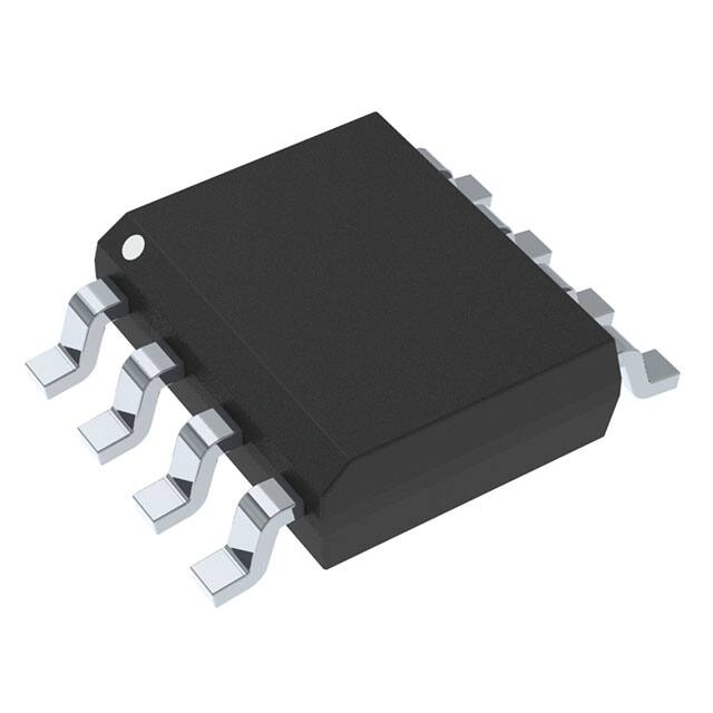
SOIC−8
CASE 751−07
STYLE 11
Features
•
•
•
•
•
•
•
•
•
•
•
•
•
•
•
•
•
Short Circuit Protection with Inrush Current Management
CMOS (3 V / 5 V) Compatible Control Input
Very Low Standby Current
Very Low Current Sense Leakage
Proportional Load Current Sense
Current Sense Enable
Off State Open Load Detection
Output Short to VD Detection
Overload and Short to Ground Indication
Thermal Shutdown with Automatic Restart
Undervoltage Shutdown
Integrated Clamp for Inductive Switching
Loss of Ground and Loss of VD Protection
ESD Protection
Reverse Battery Protection with External Components
AEC−Q100 Qualified
This is a Pb−Free Device
MARKING DIAGRAM
8
84140
ALYWG
G
1
84140
A
L
Y
W
G
(Note: Microdot may be in either location)
PIN CONNECTIONS
IN
Typical Applications
• Switch a Variety of Resistive, Inductive and Capacitive Loads
• Can Replace Electromechanical Relays and Discrete Circuits
• Automotive / Industrial
FEATURE SUMMARY
1
VD
CS_EN
OUT
GND
OUT
CS
VD
(Top View)
ORDERING INFORMATION
RDSon (typical) TJ = 25°C
RON
Output Current Limit (typical)
OFF−state Supply Current (max)
= Specific Device Code
= Assembly Location
= Wafer Lot
= Year
= Work Week
= Pb−Free Package
140
mW
Device
Package
Shipping†
NCV84140DR2G
SOIC−8
(Pb−Free)
2500 / Tape &
Reel
Ilim
12
A
ID(off)
0.5
mA
†For information on tape and reel specifications,
including part orientation and tape sizes, please
refer to our Tape and Reel Packaging Specification
Brochure, BRD8011/D.
© Semiconductor Components Industries, LLC, 2019
January, 2020 − Rev. 1
1
Publication Order Number:
NCV84140/D
�NCV84140
BLOCK DIAGRAM & PIN CONFIGURATION
VD
Overvoltage
Protection
Undervoltage
Protection
IN
Output
Clamping
Regulated
Charge Pump
í
CS_
EN
Current Limit
Overtemperature
and
Power Protection
OFF State Open
Load Detection
Analog Fault
OUT
Control
CS
Logic
Current
Sense
Figure 1. Block Diagram
Table 1. SO8 PACKAGE PIN DESCRIPTION
Pin #
Symbol
Description
1
IN
2
CS_EN
3
GND
4
CS
Analog Current Sense Output
5
VD
Supply Voltage
6
OUT
Output
7
OUT
Output
8
VD
Logic Level Input
Current Sense Enable
Ground
Supply Voltage
www.onsemi.com
2
GND
�NCV84140
ID
VDS
IIN
VD
IN
IOUT
OUT
ICS
CS
ICS_EN
CS_EN
VD
VIN
VOUT
GND
VCS
VCS_ EN
IGND
Figure 2. Voltage and Current Conventions
Table 2. Connection suggestions for unused and or unconnected pins
Connection
Input
Output
Current Sense
Current Sense Enable
Floating
X
X
Not Allowed
X
To Ground
Through 10 kW resistor
Not Allowed
Through 1 kW Resistor
Through 10 kW resistor
IN
1
2
GND
3
CS
NCV84140
CS _ EN
4
Figure 3. Pin Configuration (Top View)
www.onsemi.com
3
8
VD
7
OUT
6
OUT
5
VD
�NCV84140
ELECTRICAL SPECIFICATIONS
Table 3. MAXIMUM RATINGS
Rating
Symbol
Value
Unit
DC Supply Voltage
VD
−0.3
38
V
Max Transient Supply Voltage (Note 1)
Load Dump − Suppresses
US *
−
45
V
Input Voltage
VIN
−10
10
V
Input Current
IIN
−5
5
mA
Reverse Ground Pin Current
IGND
−
−200
mA
Output Current (Note 2)
IOUT
−6
Internally Limited
A
Reverse CS Current
ICS
−
−200
mA
CS Voltage
VCS
VD − 41
VD
V
CS_EN Voltage
VCS_EN
−10
10
V
CS_EN Current
ICS_EN
−5
5
mA
Power Dissipation Tc = 25°C (Note 5)
Ptot
Electrostatic Discharge (Note 3)
(HBM Model 100 pF / 1500 W)
Input
Current Sense
Current Sense Enable
Output
VD
Charged Device Model
CDM−AEC−Q100−011
VESD
Single Pulse Inductive Load Switching Energy
(L = 5 mH, IL = 3.84 A, TJstart = 150°C, VD tied to GND
during inductive discharge)
W
DC
4
4
4
4
4
−
−
−
−
−
kV
kV
kV
kV
kV
750
−
V
EAS
−
36.8
mJ
TJ
−40
+150
°C
Tstorage
−55
+150
°C
Operating Junction Temperature
Storage Temperature
1.17
Stresses exceeding those listed in the Maximum Ratings table may damage the device. If any of these limits are exceeded, device functionality
should not be assumed, damage may occur and reliability may be affected.
1. Load Dump Test B (with centralized load dump suppression) according to ISO16750−2 standard. Guaranteed by design. Not tested in
production. Passed Class C (or A, B) according to ISO16750−1.
2. Reverse Output current has to be limited by the load to stay within absolute maximum ratings and thermal performance.
3. This device series incorporates ESD protection and is tested by the following methods:
ESD Human Body Model tested per AEC−Q100−002 (JS−001−2017)
Field Induced Charge Device Model ESD characterization is not performed on plastic molded packages with body sizes smaller than
2 x 2 mm due to the inability of a small package body to acquire and retain enough charge to meet the minimum CDM discharge current
waveform characteristic defined in JEDEC JS−002−2018
Table 4. THERMAL RESISTANCE RATINGS
Parameter
Thermal Resistance
Junction−to−Lead (Note 4)
Junction−to−Ambient (Note 4)
Junction−to−Ambient (Note 5)
Symbol
Max. Value
RqJL
RqJA
RqJA
29
65
106
Units
°C/W
4. 645 mm2 pad size, mounted on four−layer 1s2p PCB − FR4, 2 oz. Cu thickness for top layer and 1 oz. Cu thickness for inner layers (planes
not electrically connected)
5. 2 cm2 pad size, mounted on single−layer 1s0p PCB − FR4, 2 oz. Cu thickness
www.onsemi.com
4
�NCV84140
ELECTRICAL CHARACTERISTICS (7 V ≤ VD ≤ 28 V; −40°C ≤ TJ ≤ 150°C unless otherwise specified)
Table 5. POWER
Value
Min
Typ
Max
Unit
Operating Supply Voltage
VD
4
−
28
V
Undervoltage Shutdown
VUV
−
3.5
4
V
Undervoltage Shutdown
Hysteresis
VUV_hyst
−
0.4
−
V
IOUT = 1 A, TJ = 25°C
−
140
−
mW
IOUT = 1 A, TJ = 150°C
−
−
295
IOUT = 1 A, VD = 4.5 V, TJ = 25°C
−
−
210
OFF−state: VD = 13 V,
VIN = VOUT = 0 V, Tj = 25°C
−
0.2
0.5
mA
OFF−state: VD = 13 V,
VIN = VOUT = 0 V, Tj = 85°C
−
0.2
0.5
mA
OFF−state: VD = 13 V,
VIN = VOUT = 0 V, Tj = 125°C
−
−
3
mA
ON−state: VD = 13 V,
VIN = 5 V, IOUT = 0 A
−
1.9
3.5
mA
Rating
On Resistance
Supply Current (Note 6)
Symbol
RON
ID
Conditions
On State Ground Current
IGND(ON)
VD = 13 V, VCS_EN = 5 V
VIN = 5 V, IOUT = 1 A
−
−
6
mA
Output Leakage Current
IL
VIN = VOUT = 0 V, VD = 13 V, Tj = 25°C
0
−
0.5
mA
VIN = VOUT = 0 V, VD = 13 V, Tj = 125°C
0
−
3
Product parametric performance is indicated in the Electrical Characteristics for the listed test conditions, unless otherwise noted. Product
performance may not be indicated by the Electrical Characteristics if operated under different conditions.
6. Includes PowerMOS leakage current.
Table 6. LOGIC INPUTS (VD = 13.5 V; −40°C ≤ TJ ≤ 150°C)
Value
Rating
Symbol
Input Voltage − Low
VIN_low
Input Current − Low
IIN_low
Input Voltage − High
VIN_high
Input Current − High
IIN_high
Input Hysteresis Voltage
VIN_hyst
Input Clamp Voltage
VIN_cl
CS_EN Voltage − Low
VCSE_low
CS_EN Current − Low
ICSE_low
CS_EN Voltage − High
VCSE_high
CS_EN Current − High
ICSE_high
CS_EN Hysteresis Voltage
VCSE_hyst
CS_EN Clamp Voltage
VCSE_cl
Min
Typ
Max
Unit
−
−
0.9
V
1
−
−
mA
2.1
−
−
V
−
−
10
mA
−
0.2
−
V
IIN = 1 mA
12
13
14
V
IIN = −1 mA
−14
−13
−12
−
−
0.9
V
1
−
−
mA
2.1
−
−
V
−
−
10
mA
−
0.2
−
V
ICS_EN = 1 mA
12
13
14
V
ICS_EN = −1 mA
−14
−13
−12
Conditions
VIN = 0.9 V
VIN = 2.1 V
VCS_EN = 0.9 V
VCS_EN = 2.1 V
www.onsemi.com
5
�NCV84140
Table 7. SWITCHING CHARACTERISTICS (VD = 13 V, −40°C ≤ TJ ≤ 150°C)
Value
Rating
Symbol
Conditions
Min
Typ
Max
Unit
td_on
VIN high to 20% VOUT, RL = 13 W, TJ = 25°C
5
70
120
ms
Turn−On Delay Time
Turn−Off Delay Time
td_off
VIN low to 80% VOUT, RL = 13 W, TJ = 25°C
5
40
100
ms
Slew Rate On
dVout/dton
20% to 80% VOUT, RL = 13 W, TJ = 25°C
0.1
0.27
0.7
V / ms
Slew Rate Off
dVout/dtoff
80% to 20% VOUT, RL = 13 W, TJ = 25°C
0.1
0.35
0.7
V / ms
Turn−On Switching Loss
(Note 7)
Eon
RL = 13 W
−
0.15
0.18
mJ
Turn−Off Switching Loss
(Note 7)
Eoff
RL = 13 W
−
0.1
0.18
mJ
Differential Pulse Skew, (t(OFF)
− t(ON)) see Figure 4 (Switching
Characteristics)
tskew
RL = 13 W
−50
−
50
ms
7. Not subjected to production testing.
Table 8. OUTPUT DIODE CHARACTERISTICS
Value
Rating
Forward Voltage
Symbol
Conditions
Min
Typ
Max
Unit
VF
IOUT = −1 A, TJ = 150°C
−
−
0.7
V
Table 9. PROTECTION FUNCTIONS (Note 8) (7 V ≤ VD ≤ 18 V, −40°C ≤ TJ ≤ 150°C)
Value
Min
Typ
Max
Unit
TSD
150
175
200
°C
TSD_hyst
−
7
−
°C
Reset Temperature (Note 9)
TR
TRS+1
TRS+7
−
°C
Thermal Reset of Status (Note 9)
TRS
135
−
−
°C
Rating
Temperature Shutdown (Note 9)
Temperature Shutdown
Hysteresis (TSD − TR) (Note 9)
Delta T Temperature Limit (Note 9)
DC Output Current Limit
Symbol
Conditions
TDELTA
TJ = −40°C, VD = 13 V
−
60
−
°C
IlimH
VD = 13 V
8
12
16
A
4 V < VD < 18 V
−
−
16
A
Short Circuit Current Limit during
Thermal Cycling (Note 9)
IlimTCycling
VD = 13 V
TR < Tj < TTSD
−
4
−
A
Switch Off Output Clamp Voltage
VOUT_clamp
IOUT = 0.2 A, VIN = 0 V, L = 20 mH
VD − 41
VD − 46
VD − 52
V
VOV
VIN = 0 V, ID = 20 mA
41
46
52
V
VDS_ON
IOUT = 0.07 A
−
20
−
mV
Overvoltage Protection
Output Voltage Drop Limitation
8. To ensure long term reliability during overload or short circuit conditions, protection and related diagnostic signals must be used together
with a fitting hardware & software strategy. If the device operates under abnormal conditions, this hardware & software solution must limit
the duration and number of activation cycles.
9. Not subjected to production testing.
Table 10. OPEN−LOAD DETECTION (7 V ≤ VD ≤ 18 V, −40°C ≤ TJ ≤ 150°C)
Value
Symbol
Conditions
Min
Typ
Max
Unit
Open−load Off State
Detection Threshold
VOL
VIN = 0 V, VCS_EN = 5 V
2
−
4
V
Open−load Detection
Delay at Turn Off
td_OL_off
100
350
700
ms
Off State Output Current
IOLOFF1
VIN = 0 V, VOUT = VOL
−3
−
3
mA
td_OL
VOUT = 4 V, VIN = 0 V
VCS = 90% of VCS_High
−
5
30
ms
Rating
Output rising edge to CS rising
edge during open load
www.onsemi.com
6
�NCV84140
Table 11. CURRENT SENSE CHARACTERISTICS (7 V ≤ VD ≤ 18 V, −40°C ≤ TJ ≤ 150°C)
Value
Symbol
Conditions
Min
Typ
Max
Current Sense Ratio
K0
IOUT = 0.010 A, VCS = 0.5 V, VCS_EN = 5 V
260
−
800
Current Sense Ratio
K1
IOUT = 0.025 A, VCS = 0.5 V, VCS_EN = 5 V
265
490
720
DK1 / K1
IOUT = 0.025 A, VCS = 0.5 V, VCS_EN = 5 V
−25
−
25
K2
IOUT = 0.07 A, VCS = 4 V, VCS_EN = 5 V
270
475
675
DK2 / K2
IOUT = 0.07 A, VCS_EN = 5 V
−20
−
20
K3
IOUT = 0.15 A, VCS = 4V, VCS_EN = 5 V
275
475
625
DK3 / K3
IOUT = 0.15 A, VCS_EN = 5 V
−15
−
15
K4
IOUT = 0.7 A, VCS = 4 V, VCS_EN = 5 V
375
475
540
DK4 / K4
IOUT = 0.7 A, VCS_EN = 5 V
−10
−
10
K5
IOUT = 2 A, VCS = 4 V, VCS_EN = 5 V
420
450
480
DK5 / K5
IOUT = 2 A, VCS_EN = 5 V
−5
−
5
%
CSIlkg
IOUT = 0 A, VCS = 0 V
VCS_EN = 5 V, VIN = 0 V
−
−
1
mA
IOUT = 0 A, VCS = 0 V
VCS_EN = 5 V, VIN = 5 V
−
−
2
IOUT = 1 A, VCS = 0 V
VCS_EN = 0 V, VIN = 5 V,
−
−
0.5
CSMax
VD = 7 V, VIN = 5 V, RCS = 2.7 kW,
IOUT = 2 A, TJ = 150°C, VCS_EN = 5 V
5
−
7
V
Current Sense Voltage in Fault Condition (Note 10)
VCS_fault
VD = 13 V, VIN = 0 V, RCS = 1 k,
VOUT = 4 V, VCS_EN = 5 V
−
10
−
V
Current Sense Current in Fault Condition (Note 10)
ICS_fault
VD = 13 V, VCS= 5 V, VIN = 0 V,
VOUT = 4 V, VCS_EN = 5 V
7
20
30
mA
Output Saturation Current (Note 10)
IOUT_sat
VD = 7 V, VCS= 4 V, VIN = 5 V,
TJ = 150°C, VCS_EN = 5 V
2
−
−
A
CS_EN High to CS High Delay Time
tCS_High1
VIN = 5 V, VCS_EN = 0 to 5 V,
RCS = 1 kW, RL = 13 W
−
−
100
ms
CS_EN Low to CS Low Delay Time
tCS_Low1
VIN = 5 V, VCS_EN = 5 to 0 V,
RCS = 1 kW, RL = 13 W
−
5
25
ms
Vin High to CS High Delay Time
tCS_High2
VIN = 0 to 5 V, VCS_EN = 5 V,
RCS = 1 kW, RL = 13 W
−
100
250
ms
Vin Low to CS Low Delay Time
tCS_Low2
VIN = 5 to 0 V, VCS_EN = 5 V,
RCS = 1 kW, RL = 13 W
−
50
250
ms
DtCS_High2
VIN = 5 V, VCS_EN = 5 V
RCS = 1 kW, ICS = 90% of ICS Max
−
−
100
ms
Rating
Current Sense Ratio Drift (Note 11)
Current Sense Ratio
Current Sense Ratio Drift (Note 11)
Current Sense Ratio
Current Sense Ratio Drift (Note 11)
Current Sense Ratio
Current Sense Ratio Drift (Note 11)
Current Sense Ratio
Current Sense Ratio Drift (Note 11)
Current Sense Leakage Current
CS Max Voltage
Delay Time ID Rising Edge to Rising
Edge of CS
10. The following fault conditions included are: Over−temperature, Power Limitation, and OFF State Open−Load Detection.
11. Not subjected to production testing.
www.onsemi.com
7
Unit
%
%
%
%
�NCV84140
Table 12. TRUTH TABLE
Conditions
Input
Output
CS (VCS_EN = 5 V) (Note 12)
Normal Operation
L
H
L
H
0
ICS = IOUT/KNOMINAL
Overtemperature
L
H
L
L
0
VCS_fault
Undervoltage
L
H
L
L
0
0
Overload
H
H
H (no active current mgmt)
Cycling (active current mgmt)
ICS = IOUT/KNOMINAL
VCS_fault
Short circuit to Ground
L
H
L
L
0
VCS_fault
OFF State Open Load
L
H
VCS_fault
12. If VCS_EN is low, the Current Sense output is at a high impedance, its potential depends on leakage currents and external circuitry.
www.onsemi.com
8
�NCV84140
WAVEFORMS AND GRAPHS
Resistive Switching Characteristics
V OUT
80%
80%
dVOUT / dt (off)
dVOUT / dt (on)
20%
20%
td (on)
td (off)
V IN
t (on)
t (off)
Figure 4. Switching Characteristics
VIN
Normal Operation
t
IOUT
tOFF
tON
tON
t
VCS_EN
ICS
tCS_High2
tCS_Low1
tCS_High1
ΔtCS_High2
t
t
Figure 5. Normal Operation with Current Sense Timing Characteristics
www.onsemi.com
9
�NCV84140
V IN
D t CS_ High2
t
I OUT
I OUTMAX
90% I OUTMAX
t
ICS
I CSMAX
90% ICSMAX
t
Figure 6. Delay Response from Rising Edge of IOUT and Rising Edge of CS (for VCS_EN = 5 V)
Off−State Open − Load Delay Timing
V IN
t
VOUT
VOL
t
VCS
VCS_FAULT
t d_OL_off
Figure 7. OFF−State Open−Load Flag Delay Timing
www.onsemi.com
10
t
�NCV84140
VIN
VOUT
VOL
I OUT
VCS
VCS_Fault
t d_OL_off
t CS_Low 1
VCS_EN
Figure 8. Off−State Open−Load with Added External Components
VD − VOUT
TJ = 150°C
TJ = 25°C
TJ = −40°C
VDS_ON
VDS_ON/RDS_ON(T)
IOUT
Figure 9. Voltage Drop Limitation for VDS_ON
www.onsemi.com
11
�850
800
750
700
650
600
550
500
450
400
350
300
250
200
30
25
20
15
A. Max, −40°C ≤ TJ ≤ 150°C
10
DK/K (%)
IOUT/ICS
NCV84140
A. Max, −40°C ≤ TJ ≤ 150°C
B. Typ, −40°C ≤ TJ ≤ 150°C
C. Min, −40°C ≤ TJ ≤ 150°C
0
0.2 0.4
0.6 0.8 1.0 1.2
1.4 1.6 1.8 2.0
2.2
5
0
−5
−10
−15
−20
−25
−30
B. Min, −40°C ≤ TJ ≤ 150°C
0
0.2 0.4
0.6 0.8 1.0 1.2 1.4 1.6 1.8 2.0 2.2
IOUT (A)
IOUT (A)
Figure 10. IOUT/ICS vs. IOUT
Figure 11. Maximum Current Sense Ratio Drift
vs. Load Current
VIN
IOUT
IlimH
IlimTCycling
ICS
ICS_Fault
VCS_EN
Figure 12. Short to GND or Overload
www.onsemi.com
12
�NCV84140
VIN
t
Overload
IOUT
Current Limit during
thermal cycling
DC Output Current Limit
ILIMH
ILIMTCycling
t
TJ
TTSD
TR
TRS
ΔTJ
ΔTJ_RST
TJ_Start
t
Figure 13. How TJ progresses During Short to GND or Overload
VIN
IOUT
Overload
INOMINAL
IlimH
IlimTCycling
ICS
ICS_Fault
INOM/K
VCS_EN
Figure 14. Discontinuous Overload or Short to GND
www.onsemi.com
13
�NCV84140
Resistive short
from OUT to VD
Short from OUT
to VD
VOUT
VOL
IOUT
VCS
VCS_Fault
td_OL_off
td_OL_off
VCS_EN
Figure 15. Short Circuit from OUT to VD
www.onsemi.com
14
�NCV84140
TYPICAL CHARACTERISTICS
4.5
3.5
7.0
TJ = 150°C
6.0
3.0
2.0
TJ = 25°C
1.5
6
10
14
18
22
26
34
30
VIN = 2.1 V
10
30
50
70
90
110 130 150
VD (V)
TEMPERATURE (°C)
Figure 16. Output Leakage Current vs. VD
Voltage & Temperature, VOUT = 0 V
Figure 17. Input Current vs. Temperature
−11.0
−11.5
VIN_CLAMP (V)
13.5
VIN_CLAMP (V)
VIN = 0.9 V
3.0
2.5
2.0
−50 −30 −10
14.0
IIN = 1 mA
12.5
12.0
−12.0
−12.5
IIN = −1 mA
−13.0
−13.5
11.5
−50 −30 −10
10
30
50
70
90
−14.0
−50 −30 −10
110 130 150
10
30
50
70
90
110 130 150
TEMPERATURE (°C)
TEMPERATURE (°C)
Figure 18. Input Clamp Voltage (Positive) vs.
Temperature
Figure 19. Input Clamp Voltage (Negative) vs.
Temperature
2.1
1.7
2.0
VD = 13 V
1.6
1.9
VD = 13 V
1.5
1.8
VIN_LOW (V)
VIN_HIGH (V)
4.5
3.5
TJ = −40°C
0.5
2
5.0
4.0
1.0
0
−0.5
−2
VD = 13 V
5.5
TJ = 125°C
2.5
13.0
VIN = 5 V
6.5
IIN (mA)
IOUT_LEAKAGE (mA)
7.5
VIN = 0 V
VOUT = 0 V
4.0
1.7
1.6
1.5
1.4
1.3
1.2
1.4
1.1
1.3
1.2
−50 −30 −10
10
30
50
70
90
1.0
−50 −30 −10
110 130 150
10
30
50
70
90
110 130 150
TEMPERATURE (°C)
TEMPERATURE (°C)
Figure 20. VIN Threshold High vs. Temperature
Figure 21. VIN Threshold Low vs. Temperature
www.onsemi.com
15
�NCV84140
0.40
400
0.35
350
0.30
300
0.25
250
RON (mW)
VIN_HYSTERESIS (V)
TYPICAL CHARACTERISTICS
0.20
0.15
0.05
50
10
30
50
70
90
0
−50 −30 −10
110 130 150
50
70
90
110 130 150
Figure 22. Hysteresis Input Voltage vs.
Temperature
Figure 23. RON vs. Temperature
3.50
IOUT = 1 A
3.45
3.40
UUV (V)
300
TJ = 150°C
250
3
5
7
9
3.35
3.30
TJ = 125°C
TJ = 25°C
TJ = −40°C
3.25
3.20
−50 −30 −10
11 13 15 17 19 21 23 25 27 29
10
30
50
70
90
110 130 150
VD (V)
TEMPERATURE (°C)
Figure 24. RON vs. VD Voltage
Figure 25. Undervoltage Shutdown vs.
Temperature
0.7
0.6
30
TEMPERATURE (°C)
400
350
200
150
100
50
10
TEMPERATURE (°C)
500
450
RON (mW)
150
100
650
600
550
0.8
VD = 13 V
RLOAD = 13 W
VD = 13 V
RLOAD = 13 W
0.7
0.5
dVOUT/dtoff (V/ms)
dVOUT/dton (V/ms)
200
0.10
0
−50 −30 −10
VD = 13.5 V
IOUT = 1 A
0.4
0.3
0.2
0.6
0.5
0.4
0.3
0.2
0.1
0.1
0
−50 −30 −10
10
30
50
70
90
0
−50 −30 −10
110 130 150
10
30
50
70
90
110 130 150
TEMPERATURE (°C)
TEMPERATURE (°C)
Figure 26. Slew Rate ON vs. Temperature
Figure 27. Slew Rate OFF vs. Temperature
www.onsemi.com
16
�NCV84140
TYPICAL CHARACTERISTICS
16
2.2
VD = 13 V
15
2.1
2.0
1.9
VCS_EN_HIGH (V)
ILIM (A)
14
13
12
11
1.8
1.7
1.6
1.5
10
1.4
9
1.3
8
−50 −30 −10
10
30
50
70
90
1.2
−50 −30 −10
110 130 150
10
30
50
70
90
110 130 150
TEMPERATURE (°C)
TEMPERATURE (°C)
Figure 28. Current Limit vs. Temperature
Figure 29. CS_EN Threshold High vs.
Temperature
14.0
1.8
VD = 13 V
1.7
13.5
1.6
VCS_EN_CLAMP (V)
1.5
1.4
1.3
1.2
1.1
1.0
0.9
0.8
−50 −30 −10
13.0
ICS_EN = 1 mA
12.5
12.0
11.5
10
30
50
70
90
11.0
−50 −30 −10
110 130 150
10
30
50
70
90
110 130 150
TEMPERATURE (°C)
TEMPERATURE (°C)
Figure 30. CS_EN Threshold Low vs.
Temperature
Figure 31. CS_EN Clamp Voltage (Positive) vs.
Temperature
−11.0
−11.5
VCS_EN_CLAMP (V)
VCS_EN_LOW (V)
VD = 13 V
−12.0
−12.5
ICS_EN = −1 mA
−13.0
−13.5
−14.0
−50 −30 −10
10
30
50
70
90
110 130 150
TEMPERATURE (°C)
Figure 32. CS_EN Clamp Voltage (Negative)
vs. Temperature
www.onsemi.com
17
�NCV84140
Table 13. ISO 7637−2: 2011(E) PULSE TEST RESULTS
ISO
7637−2:2011
Test Pulse
Test Severity Levels
III
IV
Delays and Impedance
# of Pulses or Test Time
Pulse / Burst Rep. Time
1
−112
−150
2 ms, 10 W
500 pulses
0.5 s
2a
55
112
0.05 ms, 2 W
500 pulses
0.5 s
3a
−165
−220
0.1 ms, 50 W
1h
100 ms
3b
112
150
0.1 ms, 50 W
1h
100 ms
ISO
7637−2:2011
Test Pulse
Test Results
III
1
2a
IV
A
C
E
3a
A
3b
A
Class
Functional Status
A
All functions of a device perform as designed during and after exposure to disturbance.
B
All functions of a device perform as designed during exposure. However, one or more of them can go beyond speci−
fied tolerance. All functions return automatically to within normal limits after exposure is removed. Memory functions
shall remain class A.
C
One or more functions of a device do not perform as designed during exposure but return automatically to normal operation after exposure is removed.
D
One or more functions of a device do not perform as designed during exposure and do not return to normal operation
until exposure is removed and the device is reset by simple “operator/use” action.
E
One or more functions of a device do not perform as designed during and after exposure and cannot be returned to
proper operation without replacing the device.
www.onsemi.com
18
�NCV84140
APPLICATION INFORMATION
+5 V
VD
RμC
CS
RμC
ZCS
Output
Clamping
IN
ZVD
Micro
Controller
RμC
Dld
Control
Logic
CS_EN
V BAT
ZBody
OUT
Cexternal
RCS
ZESD
GND
RGND
Figure 33. Application Schematic
www.onsemi.com
19
ZL
�NCV84140
Loss of Ground Protection
When device or ECU ground connection is lost and load
is still connected to ground, the device will turn the output
OFF. In loss of ground state, the output stage is held OFF
independent of the state of the input. Input resistors are
recommended between the device and microcontroller.
* I GND +
* VD
R GND
(eq. 1)
Since this resistor can be used amongst multiple
High−Side devices, please take note the sum of the
maximum active GND currents (IGND(On)max) for each
device when sizing the resistor. Please note that if the
microprocessor GND is not shared by the device GND, then
RGND produces a shift of (IGND(On)max × RGND) in the input
thresholds and CS output values. If the calculated power
dissipation leads to too large of a resistor size or several
devices have to share the same resistor, please look at the
second solution for Reverse Battery Protection. Refer to
Figure 35 for selecting the proper RGND.
Reverse Battery Protection
Solution 1: Resistor in the GND line only
(no parallel Diode)
The following calculations are true for any type of load.
In the case for no diode in parallel with RGND, the
calculations below explain how to size the resistor.
Consider the following parameters:
–IGND Maximum = 200 mA for up to −VD = 32 V.
Where –IGND is the DC reverse current through the GND
pin and –VD is the DC reverse battery voltage.
Figure 34. Reverse Battery RGND Considerations
the input threshold and current sense values if the micro
controller ground is not common to the device ground. This
shift will not vary even in the case of multiple high−side
devices using the same resistor/diode network.
Solution 2: Diode (DGND ) in parallel with RGND in the
ground line.
A resistor value of RGND = 1 kOhm should be selected and
placed in parallel to DGND if the device drives an inductive
load. The diode (DGND) provides a ~600−700 mV shift in
www.onsemi.com
20
�NCV84140
Undervoltage Protection
The device has two under−voltage threshold levels,
VD_MIN and VUV. Switching function (ON/OFF) requires
supply voltage to be at least VD_MIN. The device features a
lower supply threshold VUV, above which the output can
remain in ON state. While all protection functions are
guaranteed when the switch is ON, diagnostic functions are
operational only within nominal supply voltage range VD.
VOUT
VUV
VD_MIN
VD
Figure 35. Undervoltage Behavior
Overvoltage Protection
automatic recovery after the supply voltage comes back to
the normal operating range. The specified parameters as
well as short circuit robustness and energy capability cannot
be guaranteed during overvoltage exposure.
The NCV84140 has two Zener diodes ZVD and ZCS,
which provide integrated overvoltage protection. ZVD
protects the logic block by clamping the voltage between
supply pin VD and ground pin GND to VZVD. ZCS limits
voltage at current sense pin CS to VD – VZCS. The output
power MOSFET’s output clamping diodes provide
protection by clamping the voltage across the MOSFET
(between VD pin and OUT pin) to VCLAMP. During
overvoltage protection, current flowing through ZVD, ZCS
and the output clamp must be limited. Load impedance ZL
limits the current in the body diode ZBody. In order to limit
the current in ZVD a resistor, RGND (150 W), is required in
the GND path. External resistors RCS and RSENSE limit the
current flowing through ZCS and out of the CS pin into the
micro−controller I/O pin. With RGND, the GND pin voltage
is elevated to VD – VZVD when the supply voltage VD rises
above VZVD. ESD diodes ZESD pull up the voltage at logic
pins IN, CS_EN close to the GND pin voltage VD – VZVD.
External resistors RIN, and RCS_EN are required to limit the
current flowing out of the logic pins into the
micro−controller I/O pins. During overvoltage exposure, the
device transitions into a self−protection state, with
Overload Protection
Current limitation as well as overtemperature shutdown
mechanisms are integrated into NCV84140 to provide
protection from overload conditions such as bulb inrush or
short to ground.
Current Limitation
In case of overload, NCV84140 limits the current in the
output power MOSFET to a safe value. Due to high power
dissipation during current limitation, the device’s junction
temperature increases rapidly. In order to protect the device,
the output driver is shut down by one of the two
overtemperature protection mechanisms. The output current
limit is dependent on the device temperature, and will fold
back once the die reaches thermal shutdown. If the input
remains active during the shutdown, the output power
MOSFET will automatically be re−activated after a
minimum OFF time or when the junction temperature
returns to a safe level.
www.onsemi.com
21
�NCV84140
Output Clamping with Inductive Load Switch Off
relative to the supply voltage VBAT. During output clamping
with inductive load switch off, the energy stored in the
inductance is rapidly dissipated in the device resulting in
high power dissipation. This is a stressful condition for the
device and the maximum energy allowed for a given load
inductance should not be exceeded in any application.
The output voltage VOUT drops below GND potential
when switching off inductive loads. This is because the
inductance develops a negative voltage across the load in
response to a decaying current. The integrated clamp of the
device clamps the negative output voltage to a certain level
VIN
t
IOUT
t
VOUT
VBAT
t
VCLAMP
VBAT − VCLAMP
Figure 36. Inductive Load Switching
10
VD = 13.5 V
RL = 0 W
TJSTART = 150°C,
Single Pulse
IL (A)
TJSTART = 100°C,
Repetitive Pulse
TJSTART = 125°C,
Repetitive Pulse
1
1
10
L (mH)
Figure 37. Maximum Switch−Off Current vs. Load Inductance, VD = 13.5 V, RL = 0 W
www.onsemi.com
22
100
�NCV84140
Open Load Detection in OFF State
Open load diagnosis in OFF state can be performed by
activating an external resistive pull−up path (RPU) to VBAT.
To calculate the pull−up resistance, external leakage
currents (designed pull−down resistance, humidity−induced
leakage etc) as well as the open load threshold voltage VOL
have to be taken into account.
VBAT
VD
VOL_OFF
IN
ZBODY
ICS_FAULT
RPU
OUT
CS
RPD
GND
RCS
RLEAK
ZL
RGND
Figure 38. Open Load Detection in Off State
Current Sense in PWM Mode
When operating in PWM mode, the current sense
functionality can be used, but the timing of the input signal
and the response time of the current sense need to be
considered. When operating in PWM mode, the following
performance is to be expected. The CS_EN pin should be
held high to eliminate any unnecessary delay time to the
circuit. When VIN switches from low to high, there will be
a typical delay (tCS_High2) before the current sense responds.
Once this timing delay has passed, the rise time of the current
sense output (DtCS_High2) also needs to be considered. When
VIN switches from high to low a delay time (tCS_Low1) needs
to be considered. As long as these timing delays are allowed,
the current sense pin can be operated in PWM mode.
EMC Performance
If better EMC performance is needed, connect a C1 =
100 nF, C2 = C3 = 10 nF ceramic capacitors to the pins as
close to the device as possible according to Figure 39.
C1
VD
CS_EN
+
OUT
IN
CS
C2
GND
C3
R CS
Figure 39. EMC Capacitors Placement
www.onsemi.com
23
RL
�NCV84140
PACKAGE AND PCB THERMAL DATA
1000
R(t) (°C/W)
100
10
1
0.1
0.01
Duty Cycle = 0.5
0.2
0.1
0.05
0.02
NCV84140, 8−SOIC, PCB Copper
Area = 2 cm2, PCB:80x80x1.6 mm,
FR4, single−layer 1s0p
0.01
Single Pulse
0.000001
0.00001
0.0001
0.001
0.01
0.1
1
10
100
1000
TIME (s)
Figure 40. Junction to Ambient Transient Thermal Impedance (2 cm2 Cu Area)
100
R(t) (°C/W)
10
1
0.1
Duty Cycle = 0.5
0.2
0.1
0.05
0.02
0.01
NCV84140, 8−SOIC, PCB Copper
Area = 645 mm2, PCB:80x80x1.6 mm,
FR4, four−layer 1s2p
Single Pulse
0.01
0.001
0.000001
0.00001
0.0001
0.001
0.01
0.1
1
10
TIME (s)
Figure 41. Junction to Ambient Transient Thermal Impedance (645 mm2 Cu Area)
www.onsemi.com
24
100
1000
�MECHANICAL CASE OUTLINE
PACKAGE DIMENSIONS
SOIC−8 NB
CASE 751−07
ISSUE AK
8
1
SCALE 1:1
−X−
DATE 16 FEB 2011
NOTES:
1. DIMENSIONING AND TOLERANCING PER
ANSI Y14.5M, 1982.
2. CONTROLLING DIMENSION: MILLIMETER.
3. DIMENSION A AND B DO NOT INCLUDE
MOLD PROTRUSION.
4. MAXIMUM MOLD PROTRUSION 0.15 (0.006)
PER SIDE.
5. DIMENSION D DOES NOT INCLUDE DAMBAR
PROTRUSION. ALLOWABLE DAMBAR
PROTRUSION SHALL BE 0.127 (0.005) TOTAL
IN EXCESS OF THE D DIMENSION AT
MAXIMUM MATERIAL CONDITION.
6. 751−01 THRU 751−06 ARE OBSOLETE. NEW
STANDARD IS 751−07.
A
8
5
S
B
0.25 (0.010)
M
Y
M
1
4
−Y−
K
G
C
N
X 45 _
SEATING
PLANE
−Z−
0.10 (0.004)
H
M
D
0.25 (0.010)
M
Z Y
S
X
J
S
8
8
1
1
IC
4.0
0.155
XXXXX
A
L
Y
W
G
IC
(Pb−Free)
= Specific Device Code
= Assembly Location
= Wafer Lot
= Year
= Work Week
= Pb−Free Package
XXXXXX
AYWW
1
1
Discrete
XXXXXX
AYWW
G
Discrete
(Pb−Free)
XXXXXX = Specific Device Code
A
= Assembly Location
Y
= Year
WW
= Work Week
G
= Pb−Free Package
*This information is generic. Please refer to
device data sheet for actual part marking.
Pb−Free indicator, “G” or microdot “G”, may
or may not be present. Some products may
not follow the Generic Marking.
1.270
0.050
SCALE 6:1
INCHES
MIN
MAX
0.189
0.197
0.150
0.157
0.053
0.069
0.013
0.020
0.050 BSC
0.004
0.010
0.007
0.010
0.016
0.050
0 _
8 _
0.010
0.020
0.228
0.244
8
8
XXXXX
ALYWX
G
XXXXX
ALYWX
1.52
0.060
0.6
0.024
MILLIMETERS
MIN
MAX
4.80
5.00
3.80
4.00
1.35
1.75
0.33
0.51
1.27 BSC
0.10
0.25
0.19
0.25
0.40
1.27
0_
8_
0.25
0.50
5.80
6.20
GENERIC
MARKING DIAGRAM*
SOLDERING FOOTPRINT*
7.0
0.275
DIM
A
B
C
D
G
H
J
K
M
N
S
mm Ǔ
ǒinches
*For additional information on our Pb−Free strategy and soldering
details, please download the ON Semiconductor Soldering and
Mounting Techniques Reference Manual, SOLDERRM/D.
STYLES ON PAGE 2
DOCUMENT NUMBER:
DESCRIPTION:
98ASB42564B
SOIC−8 NB
Electronic versions are uncontrolled except when accessed directly from the Document Repository.
Printed versions are uncontrolled except when stamped “CONTROLLED COPY” in red.
PAGE 1 OF 2
ON Semiconductor and
are trademarks of Semiconductor Components Industries, LLC dba ON Semiconductor or its subsidiaries in the United States and/or other countries.
ON Semiconductor reserves the right to make changes without further notice to any products herein. ON Semiconductor makes no warranty, representation or guarantee regarding
the suitability of its products for any particular purpose, nor does ON Semiconductor assume any liability arising out of the application or use of any product or circuit, and specifically
disclaims any and all liability, including without limitation special, consequential or incidental damages. ON Semiconductor does not convey any license under its patent rights nor the
rights of others.
© Semiconductor Components Industries, LLC, 2019
www.onsemi.com
�SOIC−8 NB
CASE 751−07
ISSUE AK
DATE 16 FEB 2011
STYLE 1:
PIN 1. EMITTER
2. COLLECTOR
3. COLLECTOR
4. EMITTER
5. EMITTER
6. BASE
7. BASE
8. EMITTER
STYLE 2:
PIN 1. COLLECTOR, DIE, #1
2. COLLECTOR, #1
3. COLLECTOR, #2
4. COLLECTOR, #2
5. BASE, #2
6. EMITTER, #2
7. BASE, #1
8. EMITTER, #1
STYLE 3:
PIN 1. DRAIN, DIE #1
2. DRAIN, #1
3. DRAIN, #2
4. DRAIN, #2
5. GATE, #2
6. SOURCE, #2
7. GATE, #1
8. SOURCE, #1
STYLE 4:
PIN 1. ANODE
2. ANODE
3. ANODE
4. ANODE
5. ANODE
6. ANODE
7. ANODE
8. COMMON CATHODE
STYLE 5:
PIN 1. DRAIN
2. DRAIN
3. DRAIN
4. DRAIN
5. GATE
6. GATE
7. SOURCE
8. SOURCE
STYLE 6:
PIN 1. SOURCE
2. DRAIN
3. DRAIN
4. SOURCE
5. SOURCE
6. GATE
7. GATE
8. SOURCE
STYLE 7:
PIN 1. INPUT
2. EXTERNAL BYPASS
3. THIRD STAGE SOURCE
4. GROUND
5. DRAIN
6. GATE 3
7. SECOND STAGE Vd
8. FIRST STAGE Vd
STYLE 8:
PIN 1. COLLECTOR, DIE #1
2. BASE, #1
3. BASE, #2
4. COLLECTOR, #2
5. COLLECTOR, #2
6. EMITTER, #2
7. EMITTER, #1
8. COLLECTOR, #1
STYLE 9:
PIN 1. EMITTER, COMMON
2. COLLECTOR, DIE #1
3. COLLECTOR, DIE #2
4. EMITTER, COMMON
5. EMITTER, COMMON
6. BASE, DIE #2
7. BASE, DIE #1
8. EMITTER, COMMON
STYLE 10:
PIN 1. GROUND
2. BIAS 1
3. OUTPUT
4. GROUND
5. GROUND
6. BIAS 2
7. INPUT
8. GROUND
STYLE 11:
PIN 1. SOURCE 1
2. GATE 1
3. SOURCE 2
4. GATE 2
5. DRAIN 2
6. DRAIN 2
7. DRAIN 1
8. DRAIN 1
STYLE 12:
PIN 1. SOURCE
2. SOURCE
3. SOURCE
4. GATE
5. DRAIN
6. DRAIN
7. DRAIN
8. DRAIN
STYLE 13:
PIN 1. N.C.
2. SOURCE
3. SOURCE
4. GATE
5. DRAIN
6. DRAIN
7. DRAIN
8. DRAIN
STYLE 14:
PIN 1. N−SOURCE
2. N−GATE
3. P−SOURCE
4. P−GATE
5. P−DRAIN
6. P−DRAIN
7. N−DRAIN
8. N−DRAIN
STYLE 15:
PIN 1. ANODE 1
2. ANODE 1
3. ANODE 1
4. ANODE 1
5. CATHODE, COMMON
6. CATHODE, COMMON
7. CATHODE, COMMON
8. CATHODE, COMMON
STYLE 16:
PIN 1. EMITTER, DIE #1
2. BASE, DIE #1
3. EMITTER, DIE #2
4. BASE, DIE #2
5. COLLECTOR, DIE #2
6. COLLECTOR, DIE #2
7. COLLECTOR, DIE #1
8. COLLECTOR, DIE #1
STYLE 17:
PIN 1. VCC
2. V2OUT
3. V1OUT
4. TXE
5. RXE
6. VEE
7. GND
8. ACC
STYLE 18:
PIN 1. ANODE
2. ANODE
3. SOURCE
4. GATE
5. DRAIN
6. DRAIN
7. CATHODE
8. CATHODE
STYLE 19:
PIN 1. SOURCE 1
2. GATE 1
3. SOURCE 2
4. GATE 2
5. DRAIN 2
6. MIRROR 2
7. DRAIN 1
8. MIRROR 1
STYLE 20:
PIN 1. SOURCE (N)
2. GATE (N)
3. SOURCE (P)
4. GATE (P)
5. DRAIN
6. DRAIN
7. DRAIN
8. DRAIN
STYLE 21:
PIN 1. CATHODE 1
2. CATHODE 2
3. CATHODE 3
4. CATHODE 4
5. CATHODE 5
6. COMMON ANODE
7. COMMON ANODE
8. CATHODE 6
STYLE 22:
PIN 1. I/O LINE 1
2. COMMON CATHODE/VCC
3. COMMON CATHODE/VCC
4. I/O LINE 3
5. COMMON ANODE/GND
6. I/O LINE 4
7. I/O LINE 5
8. COMMON ANODE/GND
STYLE 23:
PIN 1. LINE 1 IN
2. COMMON ANODE/GND
3. COMMON ANODE/GND
4. LINE 2 IN
5. LINE 2 OUT
6. COMMON ANODE/GND
7. COMMON ANODE/GND
8. LINE 1 OUT
STYLE 24:
PIN 1. BASE
2. EMITTER
3. COLLECTOR/ANODE
4. COLLECTOR/ANODE
5. CATHODE
6. CATHODE
7. COLLECTOR/ANODE
8. COLLECTOR/ANODE
STYLE 25:
PIN 1. VIN
2. N/C
3. REXT
4. GND
5. IOUT
6. IOUT
7. IOUT
8. IOUT
STYLE 26:
PIN 1. GND
2. dv/dt
3. ENABLE
4. ILIMIT
5. SOURCE
6. SOURCE
7. SOURCE
8. VCC
STYLE 29:
PIN 1. BASE, DIE #1
2. EMITTER, #1
3. BASE, #2
4. EMITTER, #2
5. COLLECTOR, #2
6. COLLECTOR, #2
7. COLLECTOR, #1
8. COLLECTOR, #1
STYLE 30:
PIN 1. DRAIN 1
2. DRAIN 1
3. GATE 2
4. SOURCE 2
5. SOURCE 1/DRAIN 2
6. SOURCE 1/DRAIN 2
7. SOURCE 1/DRAIN 2
8. GATE 1
DOCUMENT NUMBER:
DESCRIPTION:
98ASB42564B
SOIC−8 NB
STYLE 27:
PIN 1. ILIMIT
2. OVLO
3. UVLO
4. INPUT+
5. SOURCE
6. SOURCE
7. SOURCE
8. DRAIN
STYLE 28:
PIN 1. SW_TO_GND
2. DASIC_OFF
3. DASIC_SW_DET
4. GND
5. V_MON
6. VBULK
7. VBULK
8. VIN
Electronic versions are uncontrolled except when accessed directly from the Document Repository.
Printed versions are uncontrolled except when stamped “CONTROLLED COPY” in red.
PAGE 2 OF 2
ON Semiconductor and
are trademarks of Semiconductor Components Industries, LLC dba ON Semiconductor or its subsidiaries in the United States and/or other countries.
ON Semiconductor reserves the right to make changes without further notice to any products herein. ON Semiconductor makes no warranty, representation or guarantee regarding
the suitability of its products for any particular purpose, nor does ON Semiconductor assume any liability arising out of the application or use of any product or circuit, and specifically
disclaims any and all liability, including without limitation special, consequential or incidental damages. ON Semiconductor does not convey any license under its patent rights nor the
rights of others.
© Semiconductor Components Industries, LLC, 2019
www.onsemi.com
�onsemi,
, and other names, marks, and brands are registered and/or common law trademarks of Semiconductor Components Industries, LLC dba “onsemi” or its affiliates
and/or subsidiaries in the United States and/or other countries. onsemi owns the rights to a number of patents, trademarks, copyrights, trade secrets, and other intellectual property.
A listing of onsemi’s product/patent coverage may be accessed at www.onsemi.com/site/pdf/Patent−Marking.pdf. onsemi reserves the right to make changes at any time to any
products or information herein, without notice. The information herein is provided “as−is” and onsemi makes no warranty, representation or guarantee regarding the accuracy of the
information, product features, availability, functionality, or suitability of its products for any particular purpose, nor does onsemi assume any liability arising out of the application or use
of any product or circuit, and specifically disclaims any and all liability, including without limitation special, consequential or incidental damages. Buyer is responsible for its products
and applications using onsemi products, including compliance with all laws, regulations and safety requirements or standards, regardless of any support or applications information
provided by onsemi. “Typical” parameters which may be provided in onsemi data sheets and/or specifications can and do vary in different applications and actual performance may
vary over time. All operating parameters, including “Typicals” must be validated for each customer application by customer’s technical experts. onsemi does not convey any license
under any of its intellectual property rights nor the rights of others. onsemi products are not designed, intended, or authorized for use as a critical component in life support systems
or any FDA Class 3 medical devices or medical devices with a same or similar classification in a foreign jurisdiction or any devices intended for implantation in the human body. Should
Buyer purchase or use onsemi products for any such unintended or unauthorized application, Buyer shall indemnify and hold onsemi and its officers, employees, subsidiaries, affiliates,
and distributors harmless against all claims, costs, damages, and expenses, and reasonable attorney fees arising out of, directly or indirectly, any claim of personal injury or death
associated with such unintended or unauthorized use, even if such claim alleges that onsemi was negligent regarding the design or manufacture of the part. onsemi is an Equal
Opportunity/Affirmative Action Employer. This literature is subject to all applicable copyright laws and is not for resale in any manner.
PUBLICATION ORDERING INFORMATION
LITERATURE FULFILLMENT:
Email Requests to: orderlit@onsemi.com
onsemi Website: www.onsemi.com
◊
TECHNICAL SUPPORT
North American Technical Support:
Voice Mail: 1 800−282−9855 Toll Free USA/Canada
Phone: 011 421 33 790 2910
Europe, Middle East and Africa Technical Support:
Phone: 00421 33 790 2910
For additional information, please contact your local Sales Representative
�