NCV8452
Self Protected High Side
Driver with Temperature
Shutdown and Current Limit
The NCV8452 is a fully protected High−Side driver that can be used
to switch a wide variety of loads, such as bulbs, solenoids and other
activators. The device is internally protected from an overload
condition by an active current limit and thermal shutdown.
www.onsemi.com
MARKING
DIAGRAM
Features
•
•
•
•
•
•
•
•
•
•
•
•
Short Circuit Protection
Thermal Shutdown with Automatic Restart
CMOS (3 V/5 V) Compatible Control Input
Overvoltage Protection and Shutdown
Output Voltage Clamp for Inductive Switching
Under Voltage Shutdown
Loss of Ground Protection
ESD Protection
Reverse Battery Protection (with external resistor)
Very Low Standby Current
NCV Prefix for Automotive and Other Applications Requiring
Unique Site and Control Change Requirements; AEC−Q101
Qualified and PPAP Capable
These Devices are Pb−Free, Halogen Free/BFR Free and are RoHS
Compliant
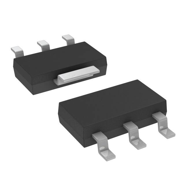
SOT−223
(TO−261)
CASE 318E
V8452
A
Y
W
G
AYW
V8452G
G
1
= Device Code
= Assembly Location
= Year
= Work Week
= Pb−Free Package
(Note: Microdot may be in either location)
ORDERING INFORMATION
See detailed ordering and shipping information in the package
dimensions section on page 12 of this data sheet.
Typical Applications
• Switch a Variety of Resistive, Inductive and Capacitive Loads
• Can Replace Electromechanical Relays and Discrete Circuits
• Automotive / Industrial
PRODUCT SUMMARY
Symbol
Characteristics
VOV
Overvoltage Protection
VD
Operation Voltage
RON
IILIM
Value
Unit
41
V
5 − 34
V
On−State Resistance
200
mW
Output Current Limit
1.0
A
© Semiconductor Components Industries, LLC, 2016
October, 2018 − Rev. 6
1
Publication Order Number:
NCV8452/D
�NCV8452
VD (Pin 4)
Overvoltage
Shutdown
Overvoltage
Protection
Undervoltage
Shutdown
Regulated
Chargepump
ESD
IN
(Pin 3)
Output
Clamping
Input
Buffer
Control
Logic
Pre
Driver
Temperature
Sensor
OUT
(Pin 1)
Current
Limitation
GND
(Pin 2)
Overtemperature
Shutdown
Figure 1. Block Diagram
PACKAGE PIN DESCRIPTION
Pin #
Symbol
Description
1
OUT
Output
2
GND
Ground
3
IN
Logic Level Input
4
VD
Supply Voltage
ID
VD
IIN
IOUT
VD
OUT
IN
GND
VIN
VOUT
IGND
Figure 2. Voltage and Current Definition
www.onsemi.com
2
�NCV8452
MAXIMUM RATINGS
Rating
Symbol
Value
Unit
VD
40
V
Vpeak
51
V
Input Voltage
VIN
−5 to VD
V
Input Current
IIN
±5
mA
IOUT
Internally Limited
A
DC Supply Voltage
Peak Transient Input Voltage
(Load Dump 37.5 V, VD = 13.5 V, ISO7637−2 pulse5) (Note 1)
Output Current
Power Dissipation
@TA = 25°C (Note 3)
@TA = 25°C (Note 4)
PD
Electrostatic Discharge (Note 1)
(HBM Model 100 pF / 1500 W)
Input
Output
VD
1.19
1.76
W
kV
±1
±5
±5
Single Pulse Inductive Load Switch Off Energy (Note 1)
(L = 4.55 H, VD = 13.5 V; IL = 0.5 A, TJstart = 25°C)
Operating Junction Temperature
Storage Temperature
EAS
0.8
J
TJ
−40 to +150
°C
Tstorage
−55 to +150
°C
Stresses exceeding those listed in the Maximum Ratings table may damage the device. If any of these limits are exceeded, device functionality
should not be assumed, damage may occur and reliability may be affected.
1. Not subjected to production testing
2. Reverse Output current has to be limited by the load to stay within absolute maximum ratings and thermal performance.
3. Minimum pad.
4. 1 in square pad size, FR−4, 1 oz Cu.
THERMAL RESISTANCE RATINGS
Parameter
Thermal Resistance (Note 5)
Junction−to−Soldering Point
Junction−to−Ambient (Note 6)
Junction−to−Ambient (Note 7)
Symbol
Max Value
Unit
RthJS
RthJA
RthJA
10
105
71
°C/W
°C/W
°C/W
5. Reverse Output current has to be limited by the load to stay within absolute maximum ratings and thermal performance.
6. Minimum pad.
7. 1 in square pad size, FR−4, 1 oz Cu.
www.onsemi.com
3
�NCV8452
ELECTRICAL CHARACTERISTICS (VD = 13.5 V; −40°C < TJ < 150°C unless otherwise specified)
Value
Rating
Symbol
Conditions
Min
Typ
Max
Unit
−
34
V
5.5
V
6.0
V
42
V
Operating Supply Voltage
VD
5
Undervoltage Shutdown
VUV
2.5
Undervoltage Restart
VUV(res)
Undervoltage Hysteresis
VUV(hyst)
Overvoltage Shutdown
0.3
VOV
34
Overvoltage Restart
VOV(res)
33
On−state Resistance
RON
IOUT = 0.5 A, VIN = 5 V, TJ = 25°C
IOUT = 0.5 A, VIN = 5 V, TJ = 150°C
160
−
200
400
mW
Standby Current
ID(off)
VIN = VOUT = 0 V
12
25
mA
Active Ground Current
IGND(on)
VIN = 5 V
1
1.8
mA
Output Leakage Current
IOUT(off)
VIN = 0 V
2
mA
0.8
V
INPUT CHARACTERISTICS
Input Voltage − Low
VIN(low)
Input Voltage − High
VIN(high)
2.2
V
Off State Input Current
IIN(off)
VIN = 0.7 V
10
mA
On State Input Current
IIN(on)
VIN = 5.0 V
10
mA
Input Threshold Hysteresis
Input Resistance
VIN(hyst)
0.3
RI
1.5
V
2.8
3.5
kW
ms
SWITCHING CHARACTERISTICS
Turn−On Time
ton
to 90% VOUT, RL = 24 W
60
120
Turn−Off Time
toff
to 10% VOUT, RL = 24 W
60
120
ms
Slew Rate On
dVOUT/dton
10% to 30% VOUT, RL = 24 W
1
4
V / ms
Slew Rate Off
dVOUT/dtoff
70% to 40% VOUT, RL = 24 W
1
4
V / ms
Reverse Battery
−VD
Requires a 150 W
Resistor in GND Connection
32
V
Forward Voltage
VF
TJ = 150°C
REVERSE BATTERY (Note 8)
0.6
V
PROTECTION FUNCTIONS (Note 9)
Temperature Shutdown (Note 8)
Temperature Shutdown Hysteresis
(Note 8)
Overvoltage Protection
TSD
150
TSD(hyst)
175
200
10
VOV
ID = 4 mA
41
Switch Off Output Clamp Voltage
VCLAMP
ID = 4 mA, VIN = 0 V
VD −
41
VD −
47
Output Current Limit Initial Peak
ILIM
VD = 20 V, TJ = 25°C
TJ = −40°C to150°C
1.0
1.8
−
°C
°C
V
V
3
A
8. Not subjected to production testing
9. To ensure long term reliability under heavy overload or short circuit conditions, protection and related diagnostic signals must be used
together with a proper hardware/software strategy. If the devices operates under abnormal conditions this hardware/software solutions must
limit the duration and number of activation cycles.
www.onsemi.com
4
�NCV8452
VBAT
VDD
VDD
Micro Controller
VD
OUT
NCV8452
IN
OUT
GND
VSS
Load
RGND
Figure 3. Application Diagram
VIN
t
ton
VOUT
toff
90%
70%
dVOUT/dtoff
dVOUT/dton
40%
30%
10%
10%
Figure 4. Resistive Load Switching Waveform
www.onsemi.com
5
t
�NCV8452
TYPICAL CHARACTERISTIC CURVES
20
18
25°C
16
14
150°C
−40°C
12
VD = 13.5 V
12
ID(off) (mA)
ID(off) (mA)
100°C
VD = 35 V
16
8
10
8
VD = 5 V
6
4
0
4
2
VIN = VOUT = 0 V
5
0
10
15
20
25
30
25
50
75
100
125
150 175
Figure 6. Standby Current vs. Junction
Temperature
1.2
VIN = VOUT = 0 V
150°C
IOUT(off) (mA)
−40°C
0.4
25°C
0.2
0
100
5
10
0.8
VD = 35 V
0.6
0.4
VD = 13.5 V
0.2
15
20
25
30
35
0
−50
40
−25
0
25
50
75
100
125
150 175
VD (V)
TJ (°C)
Figure 7. Output Leakage Current vs. Supply
Voltage
Figure 8. Output Leakage Current vs. Junction
Temperature
6
VD = 13.5 V
90
VIN = VOUT = 0 V
1
100°C
0.6
IIN(on)
5
80
IIN(off), IIN(on) (mA)
150°C
70
60
50
100°C
40
25°C
30
20
0
2
4
6
8
VIN (V)
10
12
4
3
0
−50
14
IIN(off)
2
1
−40°C
10
0
0
Figure 5. Standby Current vs. Supply Voltage
0.8
0
−25
TJ (°C)
1
IOUT(off) (mA)
40
VD (V)
1.2
IIN (mA)
35
VIN = VOUT = 0 V
0
−50
Figure 9. Input Current vs. Input Voltage
VD = 13.5 V
VIN(off) = 0.7 V
VIN(on) = 5 V
−25
0
25
50
75
TJ (°C)
100
125
150 175
Figure 10. Input Current vs. Junction
Temperature
www.onsemi.com
6
�NCV8452
TYPICAL CHARACTERISTIC CURVES
2.0
1.8
2.0
−40°C
VIN = 5 V
1.6
25°C
IGND(on) (mA)
IGND(on) (mA)
1.4
1.2
1.0
100°C
0.8
0.6
150°C
0.4
1.2
VD = 13.5 V
1.0
0.8
0.6
0.4
0.2
VD = 5 V
0.2
0
5
10
15
20
25
30
35
0
−50
40
0
25
50
75
100
125
150 175
VD (V)
Figure 11. Active Ground Current vs. Supply
Voltage
Figure 12. Active Ground Current vs. Junction
Temperature
0.3
0.25
2
VIN(hyst) (V)
Turn On
1.5
Turn Off
1
0.5
0.2
0.15
0.1
0.05
VD = 13.5 V
−25
0
25
50
75
100
125
0
−50
150 175
−25
0
25
50
75
100
125
150 175
TJ (°C)
TJ (°C)
Figure 13. Input Threshold Voltage vs.
Junction Temperature
Figure 14. Input Threshold Hysteresis vs.
Junction Temperature
2
VIN(th) (V)
0
−50
−25
TJ (°C)
2.5
VIN(th) (V)
VD = 35 V
1.6
1.4
0
VIN = 5 V
1.8
1.75
Turn ON
1.5
Turn OFF
1.25
1
0.75
0.5
0.25
0
0
5
10
15
20
25
30
35
VD (V)
Figure 15. Input Threshold Voltage vs. Supply
Voltage
www.onsemi.com
7
40
�NCV8452
TYPICAL CHARACTERISTIC CURVES
5
0.35
VUV(res)
4.5
0.3
VUV
3.5
0.25
VUV(hyst) (V)
VUV, VUV(res) (V)
4
3
2.5
2
1.5
0.2
0.15
0.1
1
0.05
0.5
0
−50
VIN = 5 V
−25
0
25
50
75
TJ (°C)
100
125
0
−50
150 175
Figure 16. Under Voltage Shutdown and
Restart vs. Junction Temperature
−25
0
25
50
75
TJ (°C)
100
125
150 175
Figure 17. Under Voltage Shutdown Hysteresis
vs. Junction Temperature
45
1
VOV
40
0.9
VOV(res)
35
0.8
0.7
30
VOV(hyst) (V)
VOV, VOV(res) (V)
VIN = 5 V
25
20
15
10
0.6
0.5
0.4
0.3
0.2
5
0
−50
0.1
VIN = 5 V
−25
0
25
50
75
TJ (°C)
100
125
VIN = 5 V
0
−50 −25
0
150 175
Figure 18. Over Voltage Shutdown vs.
Junction Temperature
50
48
VIN = 0 V
ID = 4 mA
100°C
150°C
50
75
TJ (°C)
100
125
150 175
Figure 19. Over Voltage Shutdown Hysteresis
vs. Junction Temperature
50
VIN = 0 V
ID = 4 mA
25
48
VD = 13.5 V
46
25°C
VCLAMP (V)
VCLAMP (V)
VD = 35 V
−40°C
44
42
40
46
VD = 5 V
44
42
0
5
10
15
20
25
30
35
40
−50
40
VD (V)
50
75
TJ (°C)
Figure 20. Output Clamp Voltage vs. Supply
Voltage
Figure 21. Output Clamp Voltage vs. Junction
Temperature
www.onsemi.com
8
−25
0
25
100
125
150 175
�NCV8452
TYPICAL CHARACTERISTIC CURVES
450
350
VIN = 5 V
IOUT = 0.5 A
400
350
250
RON (mW)
RON (mW)
250
150°C
300
100°C
200
25°C
150
5
10
15
20
25
30
35
0
−50
40
150°C
ILIM (A)
RON (mW)
100
125
150 175
1.5
100°C
0.5
VIN = 5 V
VD = 13.5 V
0.75
1
1.25
150°C
1.0
−40°C
0.5
25°C
2.0
25°C
0.25
−40°C
2.5
100°C
100
1.5
0
1.75
VIN = 5 V
VOUT = 0 V
0
5
10
15
20
25
30
35
OUTPUT CURRENT (A)
VD (V)
Figure 24. On−state Resistance vs. Output
Current
Figure 25. Current Limit vs. Supply Voltage
140
3.0
VD = 35 V
40
RL = 24 W
−40°C
120
VD = 13.5 V
100
ton (ms)
2.0
ILIM (A)
75
3.0
150
1.5
VD = 5 V
1.0
0
−50
50
TJ (°C)
200
0.5
25
Figure 23. On−state Resistance vs. Junction
Temperature
250
2.5
0
VD (V)
300
0
0
−25
Figure 22. On−state Resistance vs. Supply
Voltage
350
50
150
50
50
0
0
200
100
−40°C
100
VIN = 5 V
VD = 13.5 V
IOUT = 0.5 A
300
100°C
80
150°C
60
40
−25
0
25°C
20
VIN = 5 V
VOUT = 0 V
25
50
75
100
125
0
150 175
0
5
10
15
20
25
30
35
TJ (°C)
VD (V)
Figure 26. Current Limit vs. Junction
Temperature
Figure 27. Turn−On Time vs. Supply Voltage
www.onsemi.com
9
40
�NCV8452
TYPICAL CHARACTERISTIC CURVES
80
70
60
dVOUT / dton (V/ms)
25°C
40
30
100°C
150°C
20
0
3
5
10
15
20
25
30
35
0.8
100°C
0.6
0.4
0
40
0
5
10
15
20
25
30
35
VD (V)
Figure 29. Slew Rate On vs. Supply Voltage
40
140
RL = 24 W
150°C
100
100°C
2
VD = 5 V
120
1.5
ton (ms)
−dVOUT / dtoff (V/ms)
150°C
1
VD (V)
−40°C
1
80
VD = 35 V
60
VD = 13.5 V
40
25°C
0.5
20
0
5
10
15
20
25
70
30
35
40
25
50
75
100
125
150 175
Figure 31. Turn−On vs. Junction Temperature
1.6
RL = 24 W
VD = 13.5 V
VD = 35 V
VD = 5 V
30
20
0
25
50
75
TJ (°C)
100
125
1
0.8
0.6
VD = 13.5 V
0.4
0
−50
150 175
VD = 35 V
1.2
0.2
−25
RL = 24 W
1.4
10
0
−50
0
Figure 30. Slew Rate Off vs. Supply Voltage
dVOUT / dton (V/ms)
40
−25
TJ (°C)
60
50
RL = 24 W
0
−50
VD (V)
80
toff (ms)
1.2
Figure 28. Turn−Off Time vs. Supply Voltage
2.5
0
25°C
−40°C
0.2
10
0
RL = 24 W
1.4
−40°C
50
toff (ms)
1.6
RL = 24 W
Figure 32. Turn−Off Time vs. Junction
Temperature
VD = 5 V
−25
0
25
50
75
TJ (°C)
100
125
150 175
Figure 33. Slew Rate On vs. Junction
Temperature
www.onsemi.com
10
�NCV8452
TYPICAL CHARACTERISTIC CURVES
3
1.0
RL = 24 W
0.8
100°C
2
−IGND (A)
−dVOUT / dtoff (V/ms)
150°C
VD = 35 V
2.5
1.5
VD = 13.5 V
1
0
−50
−25
0
25
50
75
100
125
0.4
25°C
−40°C
VD = 5 V
0.5
0.6
0.2
0
150 175
0
0.2
0.4
0.6
0.8
1.0
TJ (°C)
−VD (V)
Figure 34. Slew Rate Off vs. Junction
Temperature
Figure 35. Supply−to−Ground Reverse
Characteristics
1.2
10
5.0
VD = 13.5 V,
RL = 0 W
4.5
150°C
4.0
3.0
IL (A)
−IOUT (A)
3.5
100°C
2.5
2.0
1.5
TJstart = 25°C
1
TJstart = 150°C
−40°C
25°C
1.0
0.5
0
0
0.2
0.4
0.6
0.8
VOUT − VD (V)
1.0
0.1
10
1.2
1000
TJstart = 25°C
100
EAS (mJ)
TJstart = 150°C
10
1
1
10
100
10000
Figure 37. Single Pulse Maximum Switch Off
Current vs. Load Inductance
SHUTDOWN TIME (ms)
VD = 13.5 V,
RL = 0 W
1000
L (mH)
Figure 36. Power FET Body Forward
Characteristics
1000
100
1000
100
TJstart = −40°C
10
1
0.1
10000
RL = 0 W
No heatsink attached
TJstart = 25°C
TJstart = 150°C
TJstart = 100°C
0
5
10
15
20
VD (V)
L (mH)
Figure 38. Single Pulse Maximum Switch Off
Energy vs. Load Inductance
25
30
35
Figure 39. Initial Short−Circuit Shutdown Time
vs. Supply Voltage
www.onsemi.com
11
40
�NCV8452
140
RL = 0 W
No heatsink attached
100
120
VD = 13.5 V
10
VD = 24 V
1
1.0 oz
100
RthJA (°C/W)
SHUTDOWN TIME (ms)
1000
80
2.0 oz
60
40
VD = 34 V
20
0.1
−50
−25
0
25
50
75
100
125
0
150 175
0
TJstart (°C)
100
200
300
400
500
600
COPPER HEAT SPREADER AREA (mm2)
700
Figure 41. Junction−to−Ambient Thermal
Resistance vs. Copper Area
Figure 40. Initial Short−Circuit Shutdown Time
vs. Starting Junction Temperature
1000
Z(t)JA (°C/W)
100
10
1
Duty Cycle = 0.5
0.2
0.1
0.02
0.05
0.01
0.1
Single Pulse
0.01
0.000001
0.00001
0.0001
0.001
0.01
0.1
1
10
100
1000
PULSE TIME (sec)
Figure 42. Junction−to−Ambient Transient Thermal Impedance (minimum pad size)
ORDERING INFORMATION
Package
Shipping†
NCV8452STT1G
SOT−223
(Pb−Free)
1000 / Tape & Reel
NCV8452STT3G
SOT−223
(Pb−Free)
4000 / Tape & Reel
Device
†For information on tape and reel specifications, including part orientation and tape sizes, please refer to our Tape and Reel Packaging
Specifications Brochure, BRD8011/D.
www.onsemi.com
12
�onsemi,
, and other names, marks, and brands are registered and/or common law trademarks of Semiconductor Components Industries, LLC dba “onsemi” or its affiliates
and/or subsidiaries in the United States and/or other countries. onsemi owns the rights to a number of patents, trademarks, copyrights, trade secrets, and other intellectual property.
A listing of onsemi’s product/patent coverage may be accessed at www.onsemi.com/site/pdf/Patent−Marking.pdf. onsemi reserves the right to make changes at any time to any
products or information herein, without notice. The information herein is provided “as−is” and onsemi makes no warranty, representation or guarantee regarding the accuracy of the
information, product features, availability, functionality, or suitability of its products for any particular purpose, nor does onsemi assume any liability arising out of the application or use
of any product or circuit, and specifically disclaims any and all liability, including without limitation special, consequential or incidental damages. Buyer is responsible for its products
and applications using onsemi products, including compliance with all laws, regulations and safety requirements or standards, regardless of any support or applications information
provided by onsemi. “Typical” parameters which may be provided in onsemi data sheets and/or specifications can and do vary in different applications and actual performance may
vary over time. All operating parameters, including “Typicals” must be validated for each customer application by customer’s technical experts. onsemi does not convey any license
under any of its intellectual property rights nor the rights of others. onsemi products are not designed, intended, or authorized for use as a critical component in life support systems
or any FDA Class 3 medical devices or medical devices with a same or similar classification in a foreign jurisdiction or any devices intended for implantation in the human body. Should
Buyer purchase or use onsemi products for any such unintended or unauthorized application, Buyer shall indemnify and hold onsemi and its officers, employees, subsidiaries, affiliates,
and distributors harmless against all claims, costs, damages, and expenses, and reasonable attorney fees arising out of, directly or indirectly, any claim of personal injury or death
associated with such unintended or unauthorized use, even if such claim alleges that onsemi was negligent regarding the design or manufacture of the part. onsemi is an Equal
Opportunity/Affirmative Action Employer. This literature is subject to all applicable copyright laws and is not for resale in any manner.
PUBLICATION ORDERING INFORMATION
LITERATURE FULFILLMENT:
Email Requests to: orderlit@onsemi.com
onsemi Website: www.onsemi.com
◊
TECHNICAL SUPPORT
North American Technical Support:
Voice Mail: 1 800−282−9855 Toll Free USA/Canada
Phone: 011 421 33 790 2910
Europe, Middle East and Africa Technical Support:
Phone: 00421 33 790 2910
For additional information, please contact your local Sales Representative
�