NCV8509 Series
Voltage Regulator Sequenced Linear, Dual
The NCV8509 Series are dual voltage regulators whose output
voltages power up in such a manner as to protect the integrity of
modern day microcontroller I/O and ESD input structures. Newer
generation microcontrollers require two power supplies. One voltage
is used for powering the core, while the other powers the I/O.
http://onsemi.com
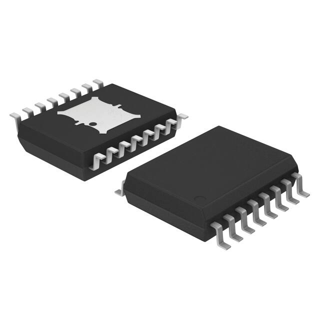
SOIC 16 LEAD
WIDE BODY
EXPOSED PAD
PDW SUFFIX
CASE 751AG
Features
• Power−Up Sequence
• Output Voltage Options:
16
VOUT1 5 V (±2%) 115 mA, VOUT2 2.6 V (2%) 100 mA
♦ VOUT1 5 V (±2%) 115 mA, VOUT2 2.5 V (2%) 100 mA
♦ VOUT1 3.3 V (±2%) 115 mA, VOUT2 1.8 V (2%) 100 mA
Low 175 mA Quiescent Current
Power Shunt
Programmable RESET Time
Dual Drive RESET Valid
Programmable SLEW Rate Control
Thermal Shutdown
16 Lead SOW Exposed Pad
NCV Prefix, for Automotive and Other Applications Requiring Site
and Change Control
AEC Qualified
PPAP Capable
These are Pb−Free Devices
1
♦
•
•
•
•
•
•
•
•
•
•
•
Typical Applications
• Automotive Powertrain
• Telematics
VBAT
CIN2
0.1 μF
VIN2
VOUT1
VOUT2
NCV8509
SLEW
CVOUT1
10 μF
CVOUT2
10 μF
RRESET
10 k
CSLEW
33 nF
Microprocessor
VIN1
REX
138 Ω
16
NCV8509xx
AWLYYWWG
1
xx
Below:
A
WL
YY
WW
G
= Voltage Ratings as Indicated
26 = 5 V/2.6 V
25 = 5 V/2.5 V
18 = 3.3 V/1.8 V
= Assembly Location
= Wafer Lot
= Year
= Work Week
= Pb−Free Device
PIN CONNECTIONS
MRA4004T3
CIN1
10 μF
MARKING DIAGRAM
GND
1
16
NC
VOUT1
NC
VIN1
VIN2
NC
VOUT2
NC
ORDERING INFORMATION
RESET
Delay
SLEW
Delay
GND
NC
NC
RESET
NC
NC
See detailed ordering and shipping information in the package
dimensions section on page 17 of this data sheet.
CDelay
33 nF
Figure 1. Application Diagram
© Semiconductor Components Industries, LLC, 2008
October, 2019 − Rev. 25
1
Publication Order Number:
NCV8509/D
�NCV8509 Series
MAXIMUM RATINGS
Rating
Value
Unit
−0.3 to 50
V
VIN1 Peak Transient Voltage
50
V
VIN2 (dc)
50
V
VIN2 (Current out of pin)
10
mA
Operating Voltage
50
V
−0.3 to 10
V
VOUT1
10
V
VOUT2
10
V
Electrostatic Discharge (Human Body Model)
(Machine Model)
4.0
400
kV
V
16
57
°C/W
°C/W
240 peak (Note 2)
°C
VIN1 (dc)
Input Voltage Range (SLEW, RESET, Delay)
Package Thermal Resistance, SOW−16 E Pad:
Junction−to−Case, RθJC
Junction−to−Ambient, RθJA
Lead Temperature Soldering:
Reflow: (SMD styles only) (Note 1)
Stresses exceeding Maximum Ratings may damage the device. Maximum Ratings are stress ratings only. Functional operation above the
Recommended Operating Conditions is not implied. Extended exposure to stresses above the Recommended Operating Conditions may affect
device reliability.
1. 60 second maximum above 183°C.
2. −5°C/+0°C allowable conditions.
ELECTRICAL CHARACTERISTICS (6.0 V < VIN1 < 18 V, IVOUT1 = 5.0 mA, IVOUT2 = 5.0 mA, −40°C < TJ < 125°C,
CVOUT1 = CVOUT2 = 10 mF; unless otherwise noted.)
Test Conditions
Characteristic
Min
Typ
Max
Unit
4.9
3.234
5.0
3.3
5.1
3.366
V
V
VOUT1
Output Voltage
5 V Option
3.3 V Option
1.0 mA < IVOUT1 < 100 mA
1.0 mA < IVOUT1 < 100 mA
Dropout Voltage (VIN1 − VOUT1)
IOUT = 100 mA
IOUT = 100 μA
−
−
400
100
600
200
mV
mV
Load Regulation
1.0 mA < IVOUT1 < 100 mA
−
10
50
mV
Line Regulation
6.0 V < VIN1 < 18 V
−
10
50
mV
Current Limit
VOUT1 = VOUT1 (typ) − 500 mV
VOUT1 = 0 V
115
−
305
105
610
300
mA
mA
VOUT2
Output Voltage
2.6 V Option
2.5 V Option
1.8 V Option
1.0 mA < IVOUT2 < 100 mA
1.0 mA < IVOUT2 < 100 mA
1.0 mA < IVOUT2 < 100 mA
2.548
2.450
1.764
2.6
2.5
1.8
2.652
2.550
1.836
V
V
V
Load Regulation
1.0 mA < IVOUT2 < 100 mA
−
5.0
50
mV
Line Regulation
6.0 V < VIN1 = VIN2 < 18 V
Current Limit
VOUT2 = VOUT2 (typ) − 500 mV
VOUT2 = 0 V
−
10
50
mV
105
−
305
105
610
300
mA
mA
−
−
125
5.0
175
10
μA
mA
150
180
210
°C
General
Quiescent Current
IOUT1 = IOUT2 = 100 μA, VIN1 = 12 V
IOUT1 = IOUT2 = 50 mA, VIN1 = 14 V
Thermal Shutdown (Note 3)
(Guaranteed by Design)
3. Both outputs will turn off.
http://onsemi.com
2
�NCV8509 Series
ELECTRICAL CHARACTERISTICS (continued) (6.0 V < VIN1 < 18 V, IVOUT1 = 5.0 mA, IVOUT2 = 5.0 mA, −40°C < TJ < 125°C,
CVOUT1 = CVOUT2 = 10 mF; unless otherwise noted.)
Test Conditions
Characteristic
Min
Typ
Max
Unit
4.0
6.0
8.0
μA
−
−
710
469
−
−
V/s
V/s
−
−
−
370
355
256
−
−
−
V/s
V/s
V/s
1.5
1.8
2.1
V
94.5
96.5
98.5
%
4.5
2.97
2.34
2.25
1.62
4.73
3.12
2.46
2.36
1.70
0.965 × VOUT
0.965 × VOUT
0.965 × VOUT
0.965 × VOUT
0.965 × VOUT
V
V
V
V
V
SLEW
SLEW Charging Current
SLEW = 1.0 V
VOUT1 SLEW Rate (Note 4)
5 V Option
3.3 V Option
CSLEW = 33 nF
VOUT2 SLEW Rate
2.6 V Option
2.5 V Option
1.8 V Option
CSLEW = 33 nF
SLEW Control Threshold
(See Figure 53)
RESET
RESET Threshold Increasing
(Note 5)
−
RESET Threshold Decreasing
−
5 V Option
3.3 V Option
2.6 V Option
2.5 V Option
1.8 V Option
RESET Output Low
IRESET = 1.0 mA
−
0.1
0.4
V
RESET Output Peak
Power Down (See Figure 41)
−
0.6
1.0
V
50
33
26
25
18
100
66
52
50
36
150
99
78
75
54
mV
mV
mV
mV
mV
1.125
1.5
1.875
V
4.0
6.0
8.0
μA
RESET Threshold Hysteresis
5 V Option
3.3 V Option
2.6 V Option
2.5 V Option
1.8 V Option
−
Delay
Delay Switching Threshold
−
Delay Charge Current
Delay = 1.0 V
Delay Saturation Voltage
VOUT1 Out of Regulation
−
−
0.1
V
Delay Discharge Current
Delay = 5.0 V VOUT1 out of Regulation
10
−
−
mA
COUT1 = COUT2 , IOUT1 = IOUT2
COUT1 = COUT2 , IOUT1 = IOUT2
−
−
−
−
3.2
2.8
V
V
COUT1 = COUT2 , IOUT1 = IOUT2
−
−
100
mV
Output Tracking
Delta 1 [VOUT1 − VOUT2]
5 V Option
3.3 V Option
Delta 2 [VOUT2 − VOUT1]
Power Shunt
Shunt Voltage 1 (VIN2)
VIN1 = 6.0 V, IOUT2 = 100 mA, No REX
3.3
−
4.6
V
Shunt Voltage 2 (VIN2)
VIN1 = 12 V, 1.0 mA < IOUT2 < 100 mA, No REX
3.25
4.5
5.75
V
4. Not a tested parameter.
5. RESET signal sensitive to VOUT1 and VOUT2.
http://onsemi.com
3
�NCV8509 Series
PIN DESCRIPTION
ÁÁÁÁÁÁÁÁÁÁÁÁÁÁÁÁÁÁÁÁÁÁÁÁÁÁÁÁÁÁÁÁÁÁÁ
ÁÁÁÁÁÁÁÁÁÁÁÁÁÁÁÁÁÁÁÁÁÁÁÁÁÁÁÁÁÁÁÁÁÁÁ
ÁÁÁÁÁÁÁÁÁÁÁÁÁÁÁÁÁÁÁÁÁÁÁÁÁÁÁÁÁÁÁÁÁÁÁ
ÁÁÁÁÁÁÁÁÁÁÁÁÁÁÁÁÁÁÁÁÁÁÁÁÁÁÁÁÁÁÁÁÁÁÁ
ÁÁÁÁÁÁÁÁÁÁÁÁÁÁÁÁÁÁÁÁÁÁÁÁÁÁÁÁÁÁÁÁÁÁÁ
ÁÁÁÁÁÁÁÁÁÁÁÁÁÁÁÁÁÁÁÁÁÁÁÁÁÁÁÁÁÁÁÁÁÁÁ
ÁÁÁÁÁÁÁÁÁÁÁÁÁÁÁÁÁÁÁÁÁÁÁÁÁÁÁÁÁÁÁÁÁÁÁ
ÁÁÁÁÁÁÁÁÁÁÁÁÁÁÁÁÁÁÁÁÁÁÁÁÁÁÁÁÁÁÁÁÁÁÁ
ÁÁÁÁÁÁÁÁ
ÁÁÁÁÁ
ÁÁÁÁÁÁÁÁÁÁÁÁÁÁÁÁÁÁÁÁÁÁ
ÁÁÁÁÁÁÁÁÁÁÁÁÁÁÁÁÁÁÁÁÁÁÁÁÁÁÁÁÁÁÁÁÁÁÁ
Pin No.
Symbol
Description
1
SLEW
Control for output rise time during power up. Requires capacitor to ground.
2
Delay
Timing capacitor for RESET function.
3
GND
Ground.
4, 5, 7−9, 11, 14, 16
NC
6
RESET
No connection.
Active reset (accurate to VOUT > 1.0 V).
10
VOUT2
100 mA output (±2% output voltage) for powering microprocessor core.
12
VIN2
Input voltage for VOUT2.
13
VIN1
Input voltage for VOUT1, and internal circuitry.
15
VOUT1
100 mA output (±2% output voltage) for powering microprocessor I/O.
VIN1
VREF
CIN1
SLEW
SLEW
Control
REX
VIN2
CIN2
Bandgap
& Bias
Power Shunt
CSLEW
VIN1
VBG
+
+
+
−
VREF
VOUT1
Error Amp
VREF
COUT1
Start−Up
Current
+
−
GND
+
+
+
−
−
+
VOUT1
VIN1
VBG
RESET Comp
Delay
VOUT2
Error Amp
VREF
COUT2
Start−Up
Current
VOUT1
−
+
RESET
VREF
VIN2
Thermal
Shutdown
Delay
Discharge
Latch
CDelay
Figure 2. Block Diagram
http://onsemi.com
4
�NCV8509 Series
TYPICAL PERFORMANCE CHARACTERISTICS
2.65
2.64
2.63
Voltage (V)
Voltage (V)
2.62
2.61
2.60
2.59
2.58
IVOUT1 = 5 mA
IVOUT2 = 5 mA
2.57
2.56
2.55
−40 −20
0
20
40
60
80
Temperature (°C)
100
120
140
3.37
3.36
3.35
3.34
3.33
3.32
3.31
3.30
3.29
3.28
3.27
3.26
3.25
3.24
3.23
−40 −20
Figure 3. 2.6 V Output Voltage
2.55
1.84
2.54
1.83
20
40
60
80
Temperature (°C)
100
120
140
1.82
Voltage (V)
2.52
Voltage (V)
0
Figure 4. 3.3 V Output Voltage
2.53
2.51
2.50
2.49
2.48
2.46
2.45
−40 −20
0
20
40
60
80
Temperature (°C)
100
120
1.81
1.80
1.79
1.78
IVOUT1 = 5 mA
IVOUT2 = 5 mA
2.47
IVOUT1 = 5 mA
IVOUT2 = 5 mA
1.77
1.76
−40 −20
140
Figure 5. 2.5 V Output Voltage
5.10
5.0
5.08
4.5
5.06
4.0
5.04
3.5
5.02
5.00
4.98
4.96
4.92
0
20
40
60
80
Temperature (°C)
100
40
60
80
Temperature (°C)
100
120
140
2.5
2.0
2.5 V
1.0 1.8 V
2.6 V
0.5
4.90
−40 −20
20
3.0
1.5
IVOUT1 = 5 mA
IVOUT2 = 5 mA
4.94
0
Figure 6. 1.8 V Output Voltage
VIN2 (VOLTS)
Voltage (V)
IVOUT1 = 5 mA
IVOUT2 = 5 mA
120
0
140
0
Figure 7. 5.0 V Output Voltage
2
4
Rex = ∞
6
8
10
VIN1 (VOLTS)
Figure 8. VIN2 versus VIN1
http://onsemi.com
5
12
14
16
�NCV8509 Series
TYPICAL PERFORMANCE CHARACTERISTICS
1.8
12
1.6
125°C
1.4
25°C
1.0
0.8
0.6
6
−40°C
4
0.4
2
0.2
0
25°C
8
−40°C
IQ (mA)
IQ (mA)
1.2
125°C
10
5
0
10
15
IOUT1 (mA)
0
25
20
0
10
20
Figure 9. IQ versus IOUT1
70
80
90
100
3.0
−40°C
−40°C
1.0
2.5
25°C
0.8
0.6
1.0
0.2
0.5
5
10
15
IOUT2 (mA)
20
0
25
125°C
1.5
0.4
0
25°C
2.0
125°C
IQ (mA)
IQ (mA)
40 50 60
IOUT1 (mA)
Figure 10. IQ versus IOUT1
1.2
0
30
0
10
20
Figure 11. IQ versus IOUT2
30
40 50 60
IOUT2 (mA)
70
80
90
100
Figure 12. IQ versus IOUT2
14
2.5
12
2.0
25°C
125°C
1.5
IQ (mA)
IQ (mA)
10
1.0
0
0
6
4
−40°C
0.5
125°C
−40°C
8
2
25°C
5
10
15
IOUT1, IOUT2 (mA)
20
0
25
0
Figure 13. IQ versus IOUT
(VOUT1 & VOUT2)
10
20
30
40 50 60 70
IOUT1, IOUT2 (mA)
Figure 14. IQ versus IOUT
(VOUT1 & VOUT2)
http://onsemi.com
6
80
90 100
�NCV8509 Series
TYPICAL PERFORMANCE CHARACTERISTICS
6
4.0
3.5
5
3.0
VOUT1 (V)
VOUT1 (V)
4
3
2
125°C
1
0
25°C
2.5
2.0
1.5
1.0
−40°C
0.5
0
1
2
3
5
4
7
6
0
10
9
8
125°C
0
1
25°C
2
3
−40°C
4
VIN1 (V)
2.5
2.5
2.0
2.0
VOUT2 (V)
3.0
1.5
1.0
0.5
0.5
25°C
125°C
0
1
2
3
−40°C
5
4
7
6
9
8
0
10
125°C
0
1
25°C
2
3
Figure 17. VOUT2 (2.6 V) versus VIN1
1.8
1.6
1.4
1.2
1.0
0.8
0.6
0.4
125°C
0
1
25°C
2
3
5
6
VIN1 (V)
7
8
Figure 18. VOUT2 (2.5 V) versus VIN1
2.0
0
9
10
9
10
−40°C
4
VIN1 (V)
0.2
8
1.5
1.0
0
7
Figure 16. VOUT1 (3.3 V) versus VIN1
3.0
VOUT2 (V)
VOUT2 (V)
Figure 15. VOUT1 (5 V) versus VIN1
5
6
VIN1 (V)
−40°C
4
5
6
VIN1 (V)
7
8
Figure 19. VOUT2 (1.8 V) versus VIN1
http://onsemi.com
7
9
10
�NCV8509 Series
TYPICAL PERFORMANCE CHARACTERISTICS
10
40
30
9.0
TIME (mS)
RESET DELAY TIME (mS)
35
9.5
8.5
25
20
15
10
8.0
5
7.5
−40 −20
0
80
20
40
60
TEMPERATURE (°C)
100
0
120
20
0
Figure 20. Reset Delay Time versus
Temperature
800
5V
120
140
160
5V
600
3.3 V
VOLTS/SEC
VOLTS/SEC
80
100
CDelay (nF)
700
2000
2.6 V
1000 2.5 V
500
60
Figure 21. Reset Delay Time versus CDelay
2500
1500
40
1.8 V
3.3 V
500
2.6 V
400
300 2.5 V
200 1.8 V
100
0
0
10
20
30
40 50 60
CSLEW (nF)
70
80
90
0
100
30
40
Figure 22. Slew Rate versus CSlew
450
QUIESCENT CURRENT (mA)
DROPOUT VOLTAGE (mV)
300
5 V/2.6 V
250
200
150
100
50
0
0
25
50
75
OUTPUT CURRENT (mA)
80
90
100
16
3.3 V/1.8 V
350
60
70
CSlew (nF)
Figure 23. Slew Rate versus CSlew
5 V/2.5 V
400
50
100
14
12
10
5 V/2.6 V
6
4
3.3 V/1.8 V
2
0
125
5 V/2.5 V
8
Iout1 = Iout2 = 50 mA
0
Figure 24. VOUT1 Dropout Voltage
2
4
6
8
10
12
14
OUTPUT CURRENT (mA)
Figure 25. Quiescent Current vs. VIN1
http://onsemi.com
8
16
18
�NCV8509 Series
TYPICAL PERFORMANCE CHARACTERISTICS
1000
UNSTABLE
REGION
5.0 V
2.5 V
10
2.6 V
1.8 V
10
ESR (W)
ESR (W)
100
100
3.3 V
UNSTABLE
REGION
STABLE
REGION
1
1
STABLE
REGION
0.1
0.1
CVOUT1 = 10 mF
0.01
0
10
20
30 40 50 60 70
OUTPUT CURRENT (mA)
80
90
0.01
100
Figure 26. VOUT1 Output Capacitor ESR (10 mF)
1000
3.3 V, 1.0 mF
UNSTABLE
REGION
STABLE
REGION
0
10
20
UNSTABLE
REGION
30 40 50 60 70
OUTPUT CURRENT (mA)
90
1 mF
0.01
100
UNSTABLE
REGION
UNSTABLE
REGION
1 mF
UNSTABLE
REGION
0.1
0.01
0
10
20
20
30 40 50 60 70
OUTPUT CURRENT (mA)
80
90 100
UNSTABLE
REGION
0.1 mF
1 mF
10
ESR (W)
ESR (W)
100
1 mF
0.1 mF
1
10
0
Figure 29. VOUT2 (2.6 V) Output Capacitor
ESR (0.1 mF / 1 mF)
STABLE REGION
10
1 mF
0.1 mF
Figure 28. VOUT1 Output Capacitor ESR (0.1 mF / 1 mF)
100
90 100
1
0.1
80
80
STABLE REGION
10
ESR (W)
ESR (W)
0.01
30 40 50 60 70
OUTPUT CURRENT (mA)
Figure 27. VOUT2 Output Capacitor ESR (10 mF)
5.0 V, 1.0 mF
0.1
20
5.0 V, 0.1 mF
100
1
10
0
100
3.3 V, 0.1 mF
10
CVOUT2 = 10 mF
30 40 50 60 70
OUTPUT CURRENT (mA)
0.1 mF
1
STABLE
REGION
UNSTABLE
REGION
0.1
80
0.01
90 100
Figure 30. VOUT2 (2.5 V) Output Capacitor
ESR (0.1 mF / 1 mF)
1 mF
0
10
20
30 40 50 60 70
OUTPUT CURRENT (mA)
80
90 100
Figure 31. VOUT2 (1.8 V) Output Capacitor
ESR (0.1 mF / 1 mF)
http://onsemi.com
9
�NCV8509 Series
TYPICAL PERFORMANCE CHARACTERISTICS
(Load Transient waveforms shown were measured on the 5 V/2.6 V device)
Figure 32. VOUT1 Load Transient Response
100 mA to No Load & No Load to 100 mA
Figure 33. VOUT2 Load Transient Response
100 mA to No Load & No Load to 100 mA
Figure 34. VOUT1 Load Transient Response
100 mA to No Load
Figure 35. VOUT2 Load Transient Response
100 mA to No Load
Figure 36. VOUT1 Load Transient Response
No Load to 100 mA
Figure 37. VOUT2 Load Transient Response
No Load to 100 mA
http://onsemi.com
10
�NCV8509 Series
TIMING DIAGRAMS
VIN1
Outputs are not actively discharged.
VOUT1
VOUT2
Figure 38. Response to Impulse
VIN1
VIN1
VOUT1
VOUT1
VOUT2
VOUT2
VIN1
Z(VOUT1) > Z(VOUT2)
�NCV8509 Series
CIRCUIT DESCRIPTION
VIN
VOUT1
RESET
Reset Delay
Power Up
Reset Delay
Short on
VOUT1
Reset Delay
VIN1 Fast
Turn Off
RESET
Output Peak
Figure 41. Dual Drive RESET Valid
RESET
The delay capacitor is discharged when the regulation
(RESET threshold) has been violated. This is a latched
incident. The capacitor will fully discharge and wait for the
device to regulate before going through the delay time event
again.
The RESET function gets its drive from both the input
(VIN1) and the output (VOUT1). Because of this, it is able to
maintain a more reliable reset valid signal. Most regulators
maintain a valid reset signal down to 1 V on the output
voltage. The reset on the NCV8509 is valid down to 0 V on
the output voltage VOUT1 (power is provided via VIN1) and
the reset on the NCV8509 is valid down to 0 V on the input
voltage VIN1 (power is provided via VOUT1). Refer to
Figure 41 for operation timing diagrams.
Power Shunt
REX routes some of the current used in the VOUT2 to a
second input pin (VIN2). This is accomplished by using an
internal shunt. A simplified version of this shunt is shown in
Figure 42. This has the effect of reducing the amount of
power dissipated on chip. The effects of choosing the
external resistor value are shown in Figure 43.
Selection of the optimum Rex resistor value can be done
using the following equation:
Delay Function
The reset delay circuit provides a programmable (by
external capacitor) delay on the RESET output lead.
The delay lead provides source current (typically 6.0 μA)
to the external delay capacitor during the following
proceedings:
1. During power up (once the regulation threshold
has been verified);
2. After a reset event has occurred and the device is
back in regulation.
(Vin(max) * 4.5)
Iout2(max)
When not using the power shunt, short VIN1 to VIN2.
http://onsemi.com
12
�NCV8509 Series
1.8
VIN1
1.6
1.4
REX
REX > 138
Watts
1.2
VIN2
REX = 138
1.0
0.8
0.6
Voltage
Regulator
REX < 138
0.4
0.2
0
VOUT2
IOUT2 = 100 mA
0
5
15
20
25
VIN
Figure 42. Power Shunt
Figure 43. Power On Chip
VIN1
18 V
135 Ω
10
VIN1
6.0 V
VIN1
6.0 V
135 Ω
135 Ω
100 mA
21.5 mA
VIN2
4.5 V
VIN2
3.1 V
VIN2
4.5 V
VOUT2
2.5 V
21.5 mA
VOUT2
2.5 V
100 mA
VOUT2
2.5 V
100 mA
RLOAD
Figure 44.
+
600 mV
−
RLOAD
RLOAD
Figure 45.
Figure 46.
Why Use a Power Shunt?
VIN1
6.0 V
The power shunt circuitry helps manage and optimize
power dissipation on the integrated circuit.
Figure 44 shows a 100 mA load. A 135 Ω resistor
dissipates 1.35 W as shown.
Without the power shunt, the 135 Ω resistor would run
into head room issues at 6.0 V and would only be able to
drive 21.5 mA as shown in Figure 45 before causing the
2.5 V output to collapse.
Figure 46 shows the power shunt circuitry adding the
current back in at low voltage operation. So the power is
moved off chip at high voltage where it is needed most.
To further clarify, Figure 47 shows the maximum allowed
resistor value (29 Ω) without the power shunt for 6.0 V
operation.
Figure 48 shows the scenario at high voltage. Only 290 mW
of power is dissipated off chip compared to Figure 44 with
1.35 W.
29 Ω
+
600 mV
−
100 mA
100 mA
VIN2
3.1 V
VIN2
15.1 V
VOUT2
2.5 V
100 mA
VOUT2
2.5 V
100 mA
Figure 47.
http://onsemi.com
VIN1
18 V
29 Ω
RLOAD
13
21.5 mA
78.5 mA
RLOAD
Figure 48.
�NCV8509 Series
NCV8509
Power Dissipation
NCV8509 has a power shunt circuit which reduces the
power on chip by utilizing an external resistor, REX. Thus
the power on chip, PIC, is equal to the total power, PT, minus
the power dissipated in the resistor PREX. Refer to Figure 49.
PIC + PTOTAL * PREX
Shunt
VIN1
Iq
REX
(1)
where
+
VSAT Q1
−
VZ
(2)
PTOTAL + (VIN1 * VOUT1) IOUT1
) (VIN1 * VOUT2) IOUT2 ) (VIN1
VIN2
Iq)
Control
Circuitry
Q2
and
PREX + (VIN1 * VIN2) IOUT2
(3)
Q3
VOUT2
VOUT1
IOUT2
IOUT1
GND
Figure 49.
ȡ IN1 SAT
ȧ
VIN2 + ȥVREF
ȧV * (I
Ȣ IN1 OUT2
(4)
for VIN1 t (VREF ) VSAT)
for (VREF ) VSAT) t VIN1 t (VREF ) (IOUT2
REX)
for (VREF ) (IOUT2
REX))
IOUT)) t VIN1
where VREF = VZ − VBE when Q1 is normally conducting.
Based on equation 3, the power in REX is dependent on
VIN2. (Increasing REX may require an increase in CIN2. A
careful system validation should be performed for stability).
The voltage on VIN2 is controlled by the shunt circuit, which
has three modes of operation, as seen in Figure 50.
Mode 1. At low battery VIN2 is equal to VIN1 minus the
saturation voltage of the shunt output NPN.
Mode 2. Once VIN1 rises above the reference voltage of
the shunt circuit, VIN2 will regulate at the VREF.
Mode 3. VIN2 would continue to regulate at VREF, but
since IOUT2 is not infinite, when VIN1 rises higher than the
reference voltage plus the voltage drop across the external
resistor REX, it will force VIN2 to be VIN1 − (IOUT2 × REX).
Equation 4 provides a summary for VIN2.
Combining equations 3 and 4 gives three different
equations for power across REX.
PMODE1 + (VSAT
IOUT2)
PMODE2 + (VIN1 * VREF)
PMODE3 + IOUT22
http://onsemi.com
14
IOUT2
REX
(5)
(6)
(7)
�NCV8509 Series
Max VIN Delta
I(VIN2) × REX
Shunt Off
4.5 V
Shunt On
VIN1
VIN2
Mode 1
Mode 3
VIN1 t VREF ) VSAT
VIN1 u VREF ) (IOUT2
VIN2 + VIN1 * VSAT
VIN2 + VIN1 * (IOUT2
REX)
REX)
Mode 2
VREF ) VSAT t VIN1 t VREF ) (IOUT2
REX)
VIN2 + VREF
Figure 50. VIN Shunt
Thermal Resistance,
Junction to Ambient, RqJA, (°C/W)
100
80
RqJA’s less than the calculated value in equation 2 will keep
the die temperature below 150°C.
In some cases, none of the packages will be sufficient to
dissipate the heat generated by the IC, and an external
heatsink will be required.
70
Heat Sinks
90
A heat sink effectively increases the surface area of the
package to improve the flow of heat away from the IC and
into the surrounding air.
Each material in the heat flow path between the IC and the
outside environment will have a thermal resistance. Like
series electrical resistances, these resistances are summed to
determine the value of RqJA:
60
50
40
0
200
600
400
Copper Area (mm2)
800
RqJA + RqJC ) RqCS ) RqSA
Figure 51. 16 Lead SOW (Exposed Pad), qJA as a
Function of the Pad Copper Area (2 oz. Cu
Thickness), Board Material = 0.0625, G−10/R−4
where:
RqJC = the junction−to−case thermal resistance,
RqCS = the case−to−heatsink thermal resistance, and
RqSA = the heatsink−to−ambient thermal resistance.
RqJC appears in the package section of the data sheet. Like
RqJA, it too is a function of package type. RqCS and RqSA are
functions of the package type, heatsink and the interface
between them. These values appear in heat sink data sheets
of heat sink manufacturers.
Once the value of PIC(max) is known, the maximum
permissible value of RqJA can be calculated:
T
RqJA + 150° C * A
PIC
(9)
(8)
The value of RqJA can then be compared with those in the
package section of the data sheet. Those packages with
http://onsemi.com
15
�NCV8509 Series
≈ 10 μs
VOUT1
Fast SLEW Rate >> Soft Start
≈ 10 μs
Fast SLEW Rate >> Soft Start
VOUT2
Disable Time
Decay Time Dependent
on External Load
Disable Time
Short On
VOUT1
Decay Time Dependent
on External Load
Short On
VOUT2
Figure 52. Fault Response. Note the High SLEW Rate Coming Out of Fault Conditions.
Soft Start Only Applies to a Power Up Sequence.
Slew Rate Control
Slew time can be calculated using the standard capacitor
equation.
Figure 53 shows the circuitry associated with Slew Rate
Control. The diagram highlights the control of one output for
simplicity. VOUT1 and VOUT2 are both controlled on the IC.
The slew rate capacitor (CSLEW) is charged with an
on−chip current source runing at 6.0 mA (typ.). Charging a
capacitor with a current source creates a linear voltage ramp
as shown in Figure 54.
The lowest voltage to the positive terminals of the
comparator (Error Amp) dominates the output voltage
(VOUT). Consequently, when CSLEW is fully discharged on
power up, it is the dominant factor on the positive terminal
and disables the output. The output (VOUT) follows the
linear ramp on the SLEW pin (after being gained up with R1
and R2) until VBG becomes the dominant voltage. This
occurs when SLEW = VBG + VD1 or approximately 1.8 V.
I + C dv , t +
dt
Using a 33 nF capacitor, the slew time is:
t+
V
Av + OUT
1.28 V
For a 5 V output, the gain would be:
Av +
5V
+ 3.9 VńV
1.28 V
assuming VBG = 1.28 V.
The resultant slew rate on the output is the slew rate on the
SLEW pin multiplied by the gain, or:
VIN1
(182 Vńs)
D2
(3.9 VńV) + 710 Vńs
VBG
+
+
−
VOUT
Error Amp
R1
SLEW Pin Voltage (V)
D1
SLEW
CSLEW
(33 nF)(1.8 V)
+ 9.9 ms
6 mA
The corresponding slew rate for this is 1.8 V/9.9 ms =
182 V/s ON THE SLEW PIN.
To calculate the slew rate on outputs, you must multiply
by the gain set up by R1 and R2.
Internal
Voltage
Rail ≈ 3.8 V
6.0 μA
C(DV)
I
R2
3.8
Outputs in Regulation
1.8
tSLEW
Time (ms)
Figure 53. Slew Control Circuitry
Figure 54.
http://onsemi.com
16
�NCV8509 Series
ORDERING INFORMATION
Device
NCV8509PDW18G
NCV8509PDW18R2G
3.3 V/1.8 V
NCV8509PDW25G
NCV8509PDW25R2G
5 V/2.5 V
NCV8509PDW26G
NCV8509PDW26R2G
Package
Shipping†
SOIC 16 Lead
(Pb−Free)
47 Units/Rail
SOIC 16 Lead
(Pb−Free)
1000 Tape & Reel
SOIC 16 Lead
(Pb−Free)
47 Units/Rail
SOIC 16 Lead
(Pb−Free)
1000 Tape & Reel
SOIC 16 Lead
(Pb−Free)
47 Units/Rail
SOIC 16 Lead
(Pb−Free)
1000 Tape & Reel
Output Voltage
5 V/2.6 V
†For information on tape and reel specifications, including part orientation and tape sizes, please refer to our Tape and Reel Packaging
Specifications Brochure, BRD8011/D.
http://onsemi.com
17
�MECHANICAL CASE OUTLINE
PACKAGE DIMENSIONS
SOIC 16 LEAD WIDE BODY, EXPOSED PAD
CASE 751AG
ISSUE B
SCALE 1:1
−U−
A
0.25 (0.010)
M
W
9
B
1
M
NOTES:
1. DIMENSIONING AND TOLERANCING PER ANSI
Y14.5M, 1982.
2. CONTROLLING DIMENSION: MILLIMETER.
3. DIMENSION A AND B DO NOT INCLUDE MOLD
PROTRUSION.
4. MAXIMUM MOLD PROTRUSION 0.15 (0.006) PER
SIDE.
5. DIMENSION D DOES NOT INCLUDE DAMBAR
PROTRUSION. ALLOWABLE PROTRUSION SHALL
BE 0.13 (0.005) TOTAL IN EXCESS OF THE D
DIMENSION AT MAXIMUM MATERIAL CONDITION.
6. 751R-01 OBSOLETE, NEW STANDARD 751R-02.
M
16
P
R x 45_
8
−W−
G 14
TOP VIEW
PIN 1 I.D.
PL
DETAIL E
C
F
−T−
0.10 (0.004) T
K
D 16 PL
0.25 (0.010)
T U
M
SEATING
PLANE
W
S
S
J
SIDE VIEW
DETAIL E
1
DIM
A
B
C
D
F
G
H
J
K
L
M
P
R
MILLIMETERS
MIN
MAX
10.15
10.45
7.40
7.60
2.35
2.65
0.35
0.49
0.50
0.90
1.27 BSC
3.45
3.66
0.25
0.32
0.00
0.10
4.72
4.93
0_
7_
10.05
10.55
0.25
0.75
INCHES
MIN
MAX
0.400
0.411
0.292
0.299
0.093
0.104
0.014
0.019
0.020
0.035
0.050 BSC
0.136
0.144
0.010
0.012
0.000
0.004
0.186
0.194
0_
7_
0.395
0.415
0.010
0.029
GENERIC
MARKING DIAGRAM*
H
EXPOSED PAD
DATE 31 MAY 2016
8
XXXXXXXXXX
XXXXXXXXXX
XXXXXXXXXX
AWLYYWWG
L
16
9
BOTTOM VIEW
XXXXX
A
WL
YY
WW
G
SOLDERING FOOTPRINT*
0.350
Exposed
Pad
0.175
0.050
CL
0.200
*This information is generic. Please refer to
device data sheet for actual part marking.
Pb−Free indicator, “G” or microdot “ G”,
may or may not be present.
0.188
CL
= Specific Device Code
= Assembly Location
= Wafer Lot
= Year
= Work Week
= Pb−Free Package
0.376
0.074
0.150
0.024
DIMENSIONS: INCHES
*For additional information on our Pb−Free strategy and soldering
details, please download the ON Semiconductor Soldering and
Mounting Techniques Reference Manual, SOLDERRM/D.
DOCUMENT NUMBER:
DESCRIPTION:
98AON21237D
Electronic versions are uncontrolled except when accessed directly from the Document Repository.
Printed versions are uncontrolled except when stamped “CONTROLLED COPY” in red.
SOIC−16, WB EXPOSED PAD
PAGE 1 OF 1
ON Semiconductor and
are trademarks of Semiconductor Components Industries, LLC dba ON Semiconductor or its subsidiaries in the United States and/or other countries.
ON Semiconductor reserves the right to make changes without further notice to any products herein. ON Semiconductor makes no warranty, representation or guarantee regarding
the suitability of its products for any particular purpose, nor does ON Semiconductor assume any liability arising out of the application or use of any product or circuit, and specifically
disclaims any and all liability, including without limitation special, consequential or incidental damages. ON Semiconductor does not convey any license under its patent rights nor the
rights of others.
© Semiconductor Components Industries, LLC, 2019
www.onsemi.com
�onsemi,
, and other names, marks, and brands are registered and/or common law trademarks of Semiconductor Components Industries, LLC dba “onsemi” or its affiliates
and/or subsidiaries in the United States and/or other countries. onsemi owns the rights to a number of patents, trademarks, copyrights, trade secrets, and other intellectual property.
A listing of onsemi’s product/patent coverage may be accessed at www.onsemi.com/site/pdf/Patent−Marking.pdf. onsemi reserves the right to make changes at any time to any
products or information herein, without notice. The information herein is provided “as−is” and onsemi makes no warranty, representation or guarantee regarding the accuracy of the
information, product features, availability, functionality, or suitability of its products for any particular purpose, nor does onsemi assume any liability arising out of the application or use
of any product or circuit, and specifically disclaims any and all liability, including without limitation special, consequential or incidental damages. Buyer is responsible for its products
and applications using onsemi products, including compliance with all laws, regulations and safety requirements or standards, regardless of any support or applications information
provided by onsemi. “Typical” parameters which may be provided in onsemi data sheets and/or specifications can and do vary in different applications and actual performance may
vary over time. All operating parameters, including “Typicals” must be validated for each customer application by customer’s technical experts. onsemi does not convey any license
under any of its intellectual property rights nor the rights of others. onsemi products are not designed, intended, or authorized for use as a critical component in life support systems
or any FDA Class 3 medical devices or medical devices with a same or similar classification in a foreign jurisdiction or any devices intended for implantation in the human body. Should
Buyer purchase or use onsemi products for any such unintended or unauthorized application, Buyer shall indemnify and hold onsemi and its officers, employees, subsidiaries, affiliates,
and distributors harmless against all claims, costs, damages, and expenses, and reasonable attorney fees arising out of, directly or indirectly, any claim of personal injury or death
associated with such unintended or unauthorized use, even if such claim alleges that onsemi was negligent regarding the design or manufacture of the part. onsemi is an Equal
Opportunity/Affirmative Action Employer. This literature is subject to all applicable copyright laws and is not for resale in any manner.
PUBLICATION ORDERING INFORMATION
LITERATURE FULFILLMENT:
Email Requests to: orderlit@onsemi.com
onsemi Website: www.onsemi.com
◊
TECHNICAL SUPPORT
North American Technical Support:
Voice Mail: 1 800−282−9855 Toll Free USA/Canada
Phone: 011 421 33 790 2910
Europe, Middle East and Africa Technical Support:
Phone: 00421 33 790 2910
For additional information, please contact your local Sales Representative
�