DATA SHEET
www.onsemi.com
Linear Voltage Regulator Low Dropout, Ultra-Low Iq,
Wide Input Voltage
MARKING
DIAGRAMS
1
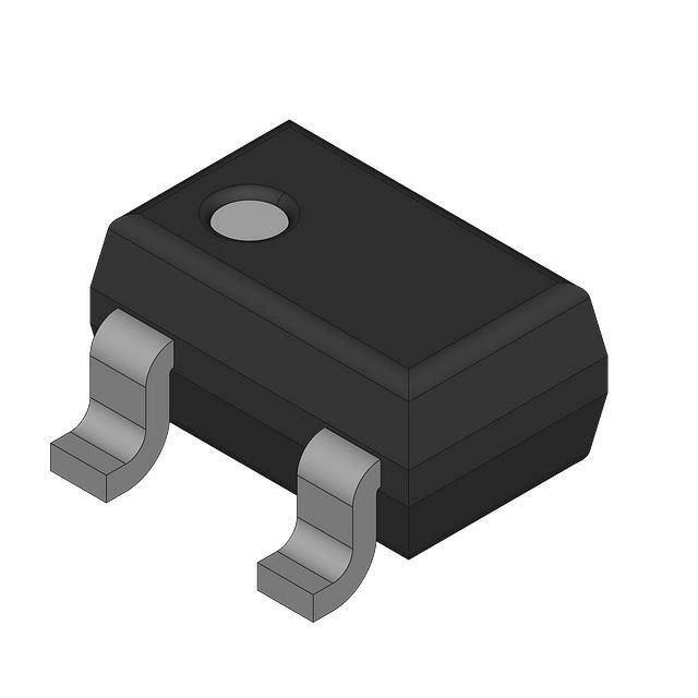
XDFN6
CASE 711AE
50 mA
XXXMG
G
NCV8715
The NCV8715 is 50 mA LDO Linear Voltage Regulator. It is a very
stable and accurate device with ultra−low ground current consumption
(4.7 mA over the full output load range) and a wide input voltage range
(up to 24 V). The regulator incorporates several protection features
such as Thermal Shutdown and Current Limiting.
Features
• Operating Input Voltage Range: 2.5 V to 24 V
• Fixed Voltage Options Available: 1.2 V to 5.0 V
• Ultra Low Quiescent Current: Max. 5.8 mA Over Full Load and
•
•
•
•
•
•
•
Temperature
±2% Accuracy Over Full Load, Line and Temperature Variations
PSRR: 52 dB at 100 kHz
Noise: 190 mVRMS from 200 Hz to 100 kHz
Thermal Shutdown and Current Limit protection
Available in XDFN6 1.5 x 1.5 mm and SC−70 (SC−88A) Package
NCV Prefix for Automotive and Other Applications Requiring
Unique Site and Control Change Requirements; AEC−Q100
Qualified and PPAP Capable; Device Temperature Grade 1: −40°C to
+125°C Ambient Operating Temperature Range
These Devices are Pb−Free, Halogen Free/BFR Free and are RoHS
Compliant
SC−70−5
(SC−88A)
CASE 419A
XXX MG
G
XXX
= Specific Device Code
M
= Date Code
G
= Pb−Free Package
(Note: Microdot may be in either location)
ORDERING INFORMATION
See detailed ordering, marking and shipping information on
page 19 of this data sheet.
Typical Applications
• Infotainment, Audio
• Communication Systems
• Safety Systems
2.5 V < Vout < 24 V
1 mF
Ceramic
OUT
IN
1.2 V < Vout < 5 V
NCV8715
NC
GND
NC
1 mF
Ceramic
Figure 1. Typical Application Schematic
© Semiconductor Components Industries, LLC, 2016
September, 2022 − Rev. 8
1
Publication Order Number:
NCV8715/D
�NCV8715
IN
THERMAL
SHUTDOWN
UVLO
BANDGAP
REFERENCE
MOSFET
DRIVER WITH
CURRENT LIMIT
OUT
EEPROM
GND
Figure 2. Simplified Block Diagram
Figure 3. Pin Description
PIN FUNCTION DESCRIPTION
Pin No.
SC−70
XDFN6
Pin Name
5
6
OUT
Regulated output voltage pin. A small 0.47 mF ceramic capacitor is needed from this pin to
ground to assure stability.
1
2
N/C
No connection. This pin can be tied to ground to improve thermal dissipation or left disconnected.
2
3
GND
Power supply ground.
3
4
N/C
No connection. This pin can be tied to ground to improve thermal dissipation or left disconnected.
−
5
N/C
No connection. This pin can be tied to ground to improve thermal dissipation or left disconnected.
4
1
IN
Description
Input pin. A small capacitor is needed from this pin to ground to assure stability.
www.onsemi.com
2
�NCV8715
ABSOLUTE MAXIMUM RATINGS
Rating
Symbol
Value
Unit
VIN
−0.3 to 24
V
VOUT
−0.3 to 6
V
tSC
Indefinite
s
TJ(MAX)
150
°C
TA
−40 to 125
°C
Storage Temperature Range
TSTG
−55 to 150
°C
Moisture Sensitivity Level
MSL
MSL1
−
ESD Capability, Human Body Model (Note 2)
ESDHBM
2000
V
ESD Capability, Machine Model (Note 2)
ESDMM
200
V
Input Voltage (Note 1)
Output Voltage
Output Short Circuit Duration
Maximum Junction Temperature
Operating Ambient Temperature Range
Stresses exceeding Maximum Ratings may damage the device. Maximum Ratings are stress ratings only. Functional operation above the
Recommended Operating Conditions is not implied. Extended exposure to stresses above the Recommended Operating Conditions may affect
device reliability.
1. Refer to ELECTRICAL CHARACTERISTICS and APPLICATION INFORMATION for Safe Operating Area.
2. This device series incorporates ESD protection and is tested by the following methods:
ESD Human Body Model tested per EIA/JESD22−A114
ESD Machine Model tested per EIA/JESD22−A115
ESD Charged Device Model tested per EIA/JESD22−C101E
Latch up Current Maximum Rating tested per JEDEC standard: JESD78.
THERMAL CHARACTERISTICS
Rating
Symbol
Value
Unit
Thermal Characteristics, SC−70 (Note 3)
Thermal Resistance, Junction−to−Air (Note 4)
RqJA
390
°C/W
Thermal Characteristics, XDFN6 (Note 3)
Thermal Resistance, Junction−to−Air (Note 4)
RqJA
260
°C/W
3. Refer to ELECTRICAL CHARACTERISTICS and APPLICATION INFORMATION for Safe Operating Area.
4. As measured using a copper heat spreading area of 650 mm2, 1 oz copper thickness.
RECOMMENDED OPERATING CONDITIONS
Parameter
Symbol
Min
Max
Unit
Input Voltage
VIN
2.5
24
V
Junction Temperature
TJ
−40
125
°C
Functional operation above the stresses listed in the Recommended Operating Ranges is not implied. Extended exposure to stresses beyond
the Recommended Operating Ranges limits may affect device reliability.
www.onsemi.com
3
�NCV8715
ELECTRICAL CHARACTERISTICS − Voltage Version 1.2 V
−40°C ≤ TJ ≤ 125°C; VIN = 2.5 V; IOUT = 1 mA, CIN = COUT = 1.0 mF, unless otherwise noted. Typical values are at TJ = +25°C. (Note 7)
Parameter
Operating Input Voltage
Test Conditions
Symbol
Min
IOUT ≤ 10 mA
VIN
10 mA< IOUT < 50 mA
Output Voltage Accuracy
3.0 V < VIN < 24 V, 0 mA < IOUT < 50 mA
VOUT
Max
Unit
2.5
24
V
3.0
24
1.164
Typ
1.2
1.236
V
Line Regulation
2.5 V ≤ VIN ≤ 24 V, IOUT = 1 mA
RegLINE
2
10
mV
Load Regulation
IOUT = 0 mA to 50 mA
RegLOAD
5
10
mV
−
mV
200
mA
Dropout Voltage (Note 5)
Maximum Output Current
Power Supply Rejection Ratio
Output Noise Voltage
Thermal Shutdown Temperature
(Note 6)
Thermal Shutdown Hysteresis (Note 6)
VDO
(Note 8)
IOUT
0 < IOUT < 50 mA, VIN = 24 V
IGND
3.4
PSRR
60
dB
VOUT = 1.2 V, IOUT = 50 mA
f = 200 Hz to 100 kHz, COUT = 10 mF
VN
65
mVrms
Temperature increasing from TJ = +25°C
TSD
170
°C
Temperature falling from TSD
TSDH
VIN = 3.0 V, VOUT = 1.2 V
VPP = 200 mV modulation
IOUT = 1 mA, COUT= 10 mF
f = 100 kHz
100
−
15
5.8
−
°C
Product parametric performance is indicated in the Electrical Characteristics for the listed test conditions, unless otherwise noted. Product
performance may not be indicated by the Electrical Characteristics if operated under different conditions.
5. Not Characterized at VIN = 3.0 V, VOUT = 1.2 V, IOUT = 50 mA.
6. Guaranteed by design and characterization.
7. Performance guaranteed over the indicated operating temperature range by design and/or characterization production tested at TJ = TA =
25°C. Low duty cycle pulse techniques are used during testing to maintain the junction temperature as close to ambient as possible.
8. Respect SOA.
www.onsemi.com
4
�NCV8715
ELECTRICAL CHARACTERISTICS − Voltage Version 1.5 V
−40°C ≤ TJ ≤ 125°C; VIN = 2.5 V; IOUT = 1 mA, CIN = COUT = 1.0 mF, unless otherwise noted. Typical values are at TJ = +25°C. (Note 11)
Parameter
Operating Input Voltage
Test Conditions
Symbol
Min
IOUT ≤ 10 mA
VIN
10 mA < IOUT < 50 mA
Output Voltage Accuracy
3.0 V < VIN < 24 V, 0 < IOUT < 50 mA
Line Regulation
VOUT + 1 V ≤ VIN ≤ 24 V, IOUT = 1 mA
Load Regulation
IOUT = 0 mA to 50 mA
Dropout Voltage (Note 9)
Maximum Output Current
Ground Current
Power Supply Rejection Ratio
Output Noise Voltage
Thermal Shutdown Temperature
(Note 10)
Thermal Shutdown Hysteresis
(Note 10)
VOUT
Max
Unit
2.5
24
V
3.0
24
1.455
Typ
1.5
1.545
V
RegLINE
2
10
mV
RegLOAD
5
10
mV
−
mV
200
mA
5.8
mA
VDO
(Note 12)
IOUT
0 < IOUT < 50 mA, VIN = 24 V
IGND
3.4
PSRR
56
dB
VOUT = 1.5 V, IOUT = 50 mA
f = 200 Hz to 100 kHz, COUT = 10 mF
VN
75
mVrms
Temperature increasing from TJ = +25°C
TSD
170
°C
Temperature falling from TSD
TSDH
VIN = 3.0 V, VOUT = 1.5 V
VPP = 200 mV modulation
IOUT = 1 mA, COUT = 10 mF
f = 100 kHz
100
−
15
−
°C
9. Not Characterized at VIN = 3.0 V, VOUT = 1.5 V, IOUT = 50 mA.
10. Guaranteed by design and characterization.
11. Performance guaranteed over the indicated operating temperature range by design and/or characterization production tested at
TJ = TA = 25°C. Low duty cycle pulse techniques are used during testing to maintain the junction temperature as close to ambient as possible.
12. Respect SOA.
www.onsemi.com
5
�NCV8715
ELECTRICAL CHARACTERISTICS − Voltage Version 1.8 V
−40°C ≤ TJ ≤ 125°C; VIN = 2.8V; IOUT = 1 mA, CIN = COUT = 1.0 mF, unless otherwise noted. Typical values are at TJ = +25°C. (Note 15)
Parameter
Operating Input Voltage
Test Conditions
Symbol
Min
IOUT ≤10 mA
VIN
10 mA < IOUT < 50 mA
Output Voltage Accuracy
3.0 V < VIN < 24 V, 0 < IOUT < 10 mA
VOUT
Max
Unit
2.8
24
V
3.0
24
1.746
Typ
1.8
1.854
V
Line Regulation
3 V ≤ VIN ≤ 24 V, IOUT = 1 mA
RegLINE
2
10
mV
Load Regulation
IOUT = 0 mA to 50 mA
RegLOAD
5
10
mV
Dropout Voltage (Note 13)
Maximum Output Current
Ground Current
Power Supply Rejection Ratio
Output Noise Voltage
Thermal Shutdown Temperature
(Note 14)
Thermal Shutdown Hysteresis
(Note 14)
VDO
mV
(Note 16)
IOUT
0 < IOUT < 50 mA, VIN = 24 V
IGND
3.4
PSRR
60
dB
VOUT = 1.8 V, IOUT = 50 mA
f = 200 Hz to 100 kHz, COUT = 10 mF
VN
95
mVrms
Temperature increasing from TJ = +25°C
TSD
170
°C
Temperature falling from TSD
TSDH
VIN = 3.0 V, VOUT = 1.8 V
VPP = 200 mV modulation
IOUT = 1 mA, COUT =10 mF
f = 100 kHz
100
−
15
200
mA
5.8
mA
−
°C
13. Not characterized at VIN = 3.0 V, VOUT = 1.8 V, IOUT = 50 mA
14. Guaranteed by design and characterization.
15. Performance guaranteed over the indicated operating temperature range by design and/or characterization production tested at TJ = TA =
25°C. Low duty cycle pulse techniques are used during testing to maintain the junction temperature as close to ambient as possible.
16. Respect SOA.
www.onsemi.com
6
�NCV8715
ELECTRICAL CHARACTERISTICS − Voltage Version 2.1 V
−40°C ≤ TJ ≤ 125°C; VIN = 3.1V; IOUT = 1 mA, CIN = COUT = 1.0 mF, unless otherwise noted. Typical values are at TJ = +25°C. (Note 19)
Parameter
Test Conditions
Symbol
Min
Operating Input Voltage
0 < IOUT < 50 mA
VIN
3.1
Output Voltage Accuracy
3.1 V < VIN < 24 V, 0 < IOUT < 50 mA
VOUT
2.058
3.1 V ≤ VIN ≤ 24 V, IOUT = 1 mA
RegLINE
Line Regulation
3.3 V ≤ VIN ≤ 24 V, IOUT = 1 mA
Load Regulation
IOUT = 0 mA to 50 mA
Dropout Voltage (Note 17)
Maximum Output Current
Ground Current
Power Supply Rejection Ratio
Output Noise Voltage
Thermal Shutdown Temperature
(Note 18)
Thermal Shutdown Hysteresis
(Note 18)
RegLOAD
Typ
Max
Unit
24
V
2.1
2.142
V
3
45
mV
3
10
10
15
VDO
mV
mV
(Note 20)
IOUT
0 < IOUT < 50 mA, VIN = 24 V
IGND
3.4
PSRR
60
dB
VOUT = 2.1 V, IOUT = 50 mA
f = 200 Hz to 100 kHz, COUT = 10 mF
VN
105
mVrms
Temperature increasing from TJ = +25°C
TSD
170
°C
Temperature falling from TSD
TSDH
VIN = 3.1 V, VOUT = 2.1 V
VPP = 200 mV modulation
IOUT = 1 mA, COUT =10 mF
f = 100 kHz
100
−
15
200
mA
5.8
mA
−
°C
17. Not characterized at VIN = 3.1 V, VOUT = 2.1 V, IOUT = 50 mA
18. Guaranteed by design and characterization.
19. Performance guaranteed over the indicated operating temperature range by design and/or characterization production tested at TJ = TA =
25°C. Low duty cycle pulse techniques are used during testing to maintain the junction temperature as close to ambient as possible.
20. Respect SOA.
www.onsemi.com
7
�NCV8715
ELECTRICAL CHARACTERISTICS − Voltage Version 2.5 V
−40°C ≤ TJ ≤ 125°C; VIN = 3.5 V; IOUT = 1 mA, CIN = COUT = 1.0 mF, unless otherwise noted. Typical values are at TJ = +25°C. (Note 23)
Parameter
Test Conditions
Symbol
Min
Operating Input Voltage
0 < IOUT < 50 mA
VIN
3.5
Output Voltage Accuracy
3.5 V < VIN < 24 V, 0 < IOUT < 50 mA
VOUT
2.45
Line Regulation
VOUT + 1 V ≤ VIN ≤ 24 V, IOUT = 1 mA
Load Regulation
IOUT = 0 mA to 50 mA
Dropout Voltage (Note 21)
VDO = VIN – (VOUT(NOM) – 125 mV)
IOUT = 50 mA
VDO
Maximum Output Current
(Note 24)
IOUT
0 < IOUT < 50 mA, VIN = 24 V
IGND
3.4
PSRR
60
dB
VOUT = 2.5 V, IOUT = 50 mA
f = 200 Hz to 100 kHz, COUT = 10 mF
VN
115
mVrms
Temperature increasing from TJ = +25°C
TSD
170
°C
Temperature falling from TSD
TSDH
Ground Current
Power Supply Rejection Ratio
Output Noise Voltage
Thermal Shutdown Temperature
(Note 22)
Thermal Shutdown Hysteresis
(Note 22)
VIN = 3.5 V, VOUT = 2.5 V
VPP = 200 mV modulation
IOUT = 1 mA, COUT =10 mF
f = 100 kHz
Typ
Max
Unit
24
V
2.5
2.55
V
RegLINE
3
10
mV
RegLOAD
10
15
mV
260
450
mV
200
mA
5.8
mA
100
−
15
−
°C
21. Characterized when VOUT falls 125 mV below the regulated voltage and only for devices with VOUT = 2.5 V.
22. Guaranteed by design and characterization.
23. Performance guaranteed over the indicated operating temperature range by design and/or characterization production tested at
TJ = TA = 25°C. Low duty cycle pulse techniques are used during testing to maintain the junction temperature as close to ambient as possible.
24. Respect SOA.
www.onsemi.com
8
�NCV8715
ELECTRICAL CHARACTERISTICS − Voltage Version 3.0 V
−40°C ≤ TJ ≤ 125°C; VIN = 4.0 V; IOUT = 1 mA, CIN = COUT = 1.0 mF, unless otherwise noted. Typical values are at TJ = +25°C. (Note 27)
Parameter
Test Conditions
Symbol
Min
Operating Input Voltage
0 < IOUT < 50 mA
VIN
4.0
Output Voltage Accuracy
4.0 V < VIN < 24 V, 0< IOUT < 50 mA
VOUT
2.94
Typ
Max
Unit
24
V
3.0
3.06
V
Line Regulation
VOUT + 1 V ≤ VIN ≤ 24 V, IOUT = 1 mA
RegLINE
3
10
mV
Load Regulation
IOUT = 0 mA to 50 mA
RegLOAD
10
15
mV
VDO = VIN – (VOUT(NOM) – 150 mV)
IOUT = 50 mA
VDO
400
mV
200
mA
5.8
mA
Dropout voltage (Note 25)
Maximum Output Current
Ground current
Power Supply Rejection Ratio
Output Noise Voltage
Thermal Shutdown Temperature
(Note 26)
Thermal Shutdown Hysteresis
(Note 26)
250
(Note 28)
IOUT
0 < IOUT < 50 mA, VIN = 24 V
IGND
3.4
PSRR
60
dB
VOUT = 3 V, IOUT = 50 mA,
f = 200 Hz to 100 kHz, COUT = 10 mF
VN
135
mVrms
Temperature increasing from TJ = +25°C
TSD
170
°C
Temperature falling from TSD
TSDH
VIN = 4.0 V, VOUT = 3.0 V
VPP = 100 mV modulation
IOUT = 1 mA, COUT = 10 mF
f = 100 kHz
100
-
25
-
°C
25. Characterized when VOUT falls 150 mV below the regulated voltage and only for devices with VOUT = 3.0 V
26. Guaranteed by design and characterization.
27. Performance guaranteed over the indicated operating temperature range by design and/or characterization production tested
at TJ = TA = 25°C. Low duty cycle pulse techniques are used during testing to maintain the junction temperature as close to ambient as
possible.
28. Respect SOA
www.onsemi.com
9
�NCV8715
ELECTRICAL CHARACTERISTICS − Voltage Version 3.3 V
−40°C ≤ TJ ≤ 125°C; VIN = 4.3 V; IOUT = 1 mA, CIN = COUT = 1.0 mF, unless otherwise noted. Typical values are at TJ = +25°C. (Note 31)
Parameter
Test Conditions
Symbol
Min
Operating Input Voltage
0 < IOUT < 50 mA
VIN
4.3
Output Voltage Accuracy
4.3 V < VIN < 24 V, 0 < IOUT < 50 mA
VOUT
3.234
Line Regulation
VOUT + 1 V ≤ VIN ≤ 24 V, IOUT = 1 mA
Load Regulation
IOUT = 0 mA to 50 mA
VDO = VIN – (VOUT(NOM) – 165 mV)
IOUT = 50 mA
VDO
Dropout Voltage (Note 29)
Maximum Output Current
Ground Current
Power Supply Rejection Ratio
Output Noise Voltage
Thermal Shutdown Temperature
(Note 30)
Thermal Shutdown Hysteresis
(Note 30)
Typ
Max
Unit
24
V
3.3
3.366
V
RegLINE
3
10
mV
RegLOAD
10
15
mV
230
350
mV
200
mA
5.8
mA
(Note 32)
IOUT
0 < IOUT < 50 mA, VIN = 24 V
IGND
3.4
PSRR
60
dB
VOUT = 4.3 V, IOUT = 50 mA
f = 200 Hz to 100 kHz, COUT = 10 mF
VN
140
mVrms
Temperature increasing from TJ = +25°C
TSD
170
°C
Temperature falling from TSD
TSDH
VIN = 4.3 V, VOUT = 3.3 V
VPP = 200 mV modulation
IOUT = 1 mA, COUT =10 mF
f = 100 kHz
100
−
15
−
°C
29. Characterized when VOUT falls 165 mV below the regulated voltage and only for devices with VOUT = 3.3 V.
30. Guaranteed by design and characterization.
31. Performance guaranteed over the indicated operating temperature range by design and/or characterization production tested at TJ = TA =
25°C. Low duty cycle pulse techniques are used during testing to maintain the junction temperature as close to ambient as possible.
32. Respect SOA.
www.onsemi.com
10
�NCV8715
ELECTRICAL CHARACTERISTICS − Voltage Version 5.0 V
−40°C ≤ TJ ≤ 125°C; VIN = 6.0 V; IOUT = 1 mA, CIN = COUT = 1 mF, unless otherwise noted. Typical values are at TJ = +25°C. (Note 35)
Parameter
Test Conditions
Symbol
Min
Operating Input Voltage
0 < IOUT < 50 mA
VIN
6.0
Output Voltage Accuracy
6.0V < VIN < 24V, 0< IOUT < 50 mA
VOUT
4.9
Line Regulation
VOUT + 1 V ≤ VIN ≤ 24 V, Iout = 1mA
Load Regulation
IOUT = 0 mA to 50 mA
VDO = VIN – (VOUT(NOM) – 250 mV)
IOUT = 50 mA
VDO
Dropout Voltage (Note 33)
Maximum Output Current
Ground Current
Power Supply Rejection Ratio
Output Noise Voltage
Thermal Shutdown Temperature
(Note 34)
Thermal Shutdown Hysteresis
(Note 34)
Typ
Max
Unit
24
V
5.0
5.1
V
RegLINE
3
10
mV
RegLOAD
10
20
mV
230
350
mV
200
mA
5.8
mA
(Note 36)
IOUT
0 < IOUT < 50 mA, VIN = 24 V
IGND
3.4
PSRR
56
dB
VOUT = 5.0 V, IOUT = 50 mA
f = 200 Hz to 100 kHz, COUT = 10 mF
VN
190
mVrms
Temperature increasing from TJ = +25°C
TSD
170
°C
Temperature falling from TSD
TSDH
VIN = 6.0 V, VOUT = 5.0 V
VPP = 200 mV modulation
IOUT = 1 mA, COUT =10 mF
f = 100 kHz
90
−
15
−
°C
33. Characterized when VOUT falls 250 mV below the regulated voltage and only for devices with VOUT = 5.0 V.
34. Guaranteed by design and characterization.
35. Performance guaranteed over the indicated operating temperature range by design and/or characterization production tested at TJ = TA =
25°C. Low duty cycle pulse techniques are used during testing to maintain the junction temperature as close to ambient as possible.
36. Respect SOA.
www.onsemi.com
11
�NCV8715
1.2
2.506
VIN = 3.0 V
1.198
1.197
1.196
VIN = (5.0 − 24.0) V
1.195
1.194
1.193
1.192
−40
NCV8715x12xxx
CIN = COUT = 1 mF
IOUT = 1 mA
−20
0
20
VIN = 3.0 V
2.504
OUTPUT VOLTAGE (V)
OUTPUT VOLTAGE (V)
1.199
2.502
2.5
VIN = (5.0 − 24.0) V
2.498
2.496
2.494
NCV8715x25xxx
CIN = COUT = 1 mF
IOUT = 1 mA
2.492
40
60
80
100
2.49
−40
120
−20
0
3.315
5.015
3.312
5.01
OUTPUT VOLTAGE (V)
OUTPUT VOLTAGE (V)
5.02
3.309
3.306
3.303
3.294
−40
NCV8715x33xxx
CIN = COUT = 1 mF
IOUT = 1 mA
VIN = 4.3 V to 24 V
−20
0
20
40
60
80
TEMPERATURE (°C)
100
5.005
1.192
1.188
VIN = 3.0 V
VIN = 5.0 V
VIN = 10 V
VIN = 15 V
VIN = 20 V
VIN = 24 V
1.184
1.180
1.176
1.172
0
10
20
30
OUTPUT CURRENT (mA)
120
4.995
NCV8715x50xxx
CIN = COUT = 1 mF
IOUT = 1 mA
4.99
4.98
−40
0
20
40
60
80
100
JUNCTION TEMPERATURE (°C)
2.504
120
NCV8715x25xxx
CIN = COUT = 1 mF
TA = 25°C
2.500
2.496
2.492
2.488
VIN = 3.5 V
VIN = 5.0 V
VIN = 10 V
VIN = 15 V
VIN = 20 V
VIN = 24 V
2.484
2.480
2.476
40
−20
Figure 7. Output Voltage vs. Temperature
OUTPUT VOLTAGE (V)
OUTPUT VOLTAGE (V)
1.196
100
VIN = 6.0 V
5
4.985
120
NCV8715x12xxx
CIN = COUT = 1 mF
TA = 25°C
1.200
80
VIN = (8.0 − 24.0) V
Figure 6. Output Voltage vs. Temperature
1.204
60
Figure 5. Output Voltage vs. Temperature
3.318
3.297
40
TEMPERATURE (°C)
TEMPERATURE (°C)
Figure 4. Output Voltage vs. Temperature
3.3
20
50
2.472
0
Figure 8. Output Voltage vs. Output Current
10
20
30
OUTPUT CURRENT (mA)
40
Figure 9. Output Voltage vs. Output Current
www.onsemi.com
12
50
�NCV8715
NCV8715x33xxx
CIN = COUT = 1 mF
TA = 25°C
OUTPUT VOLTAGE (V)
3.308
3.304
3.300
3.296
3.292
VIN = 4.3 V
VIN = 10 V
VIN = 15 V
VIN = 20 V
VIN = 24 V
3.288
3.284
3.280
0
10
5.016
NCV8715x50xxx
CIN = COUT = 1 mF
TA = 25°C
5.008
OUTPUT VOLTAGE (V)
3.312
5.000
4.992
4.984
4.976
VIN = 6.0 V
VIN = 10 V
VIN = 15 V
VIN = 20 V
VIN = 24 V
4.968
4.960
20
30
40
4.952
50
0
10
OUTPUT CURRENT (mA)
Figure 10. Output Voltage vs. Output Current
DROPOUT VOLTAGE (mV)
TA = 125°C
250
TA = 25°C
200
150
TA = −40°C
100
50
0
300
TA = 125°C
250
TA = 25°C
200
150
100
TA = −40°C
50
0
0
10
20
30
40
0
50
10
OUTPUT CURRENT (mA)
400
GND, QUIESCENT CURRENT (mA)
TA = 125°C
250
200
TA = 25°C
150
100
TA = −40°C
50
10
40
50
40
300
0
30
Figure 13. Dropout Voltage vs. Output Current
NCV8715x50xxx
CIN = COUT = 1 mF
350
20
OUTPUT CURRENT (mA)
Figure 12. Dropout Voltage vs. Output Current
DROPOUT VOLTAGE (mV)
50
NCV8715x33xxx
CIN = COUT = 1 mF
350
300
0
40
400
NCV8715x25xxx
CIN = COUT = 1 mF
350
30
Figure 11. Output Voltage vs. Output Current
DROPOUT VOLTAGE (mV)
400
20
OUTPUT CURRENT (mA)
20
30
40
50
NCV8715x12xxx
CIN = COUT = 1 mF
TA = 25°C
35
30
25
20
15
IOUT = 0
IOUT = 50 mA
10
5
0
0
5
10
15
20
OUTPUT CURRENT (mA)
INPUT VOLTAGE (V)
Figure 14. Dropout Voltage vs. Output Current
Figure 15. Ground Current vs. Input Voltage
www.onsemi.com
13
25
�NCV8715
IOUT = 0
IOUT = 50 mA
35
40
NCV8715x25xxx
CIN = COUT = 1 mF
TA = 25°C
30
GND, QUIESCENT CURRENT (mA)
GND, QUIESCENT CURRENT (mA)
40
25
20
15
10
5
0
0
5
10
15
20
30
25
20
15
10
5
0
25
0
5
10
INPUT VOLTAGE (V)
20
25
Figure 17. Ground Current vs. Input Voltage
4.5
40
NCV8715x50xxx
CIN = COUT = 1 mF
TA = 25°C
IOUT = 0
IOUT = 50 mA
35
30
QUIESCENT CURRENT (mA)
GND, QUIESCENT CURRENT (mA)
15
INPUT VOLTAGE (V)
Figure 16. Ground Current vs. Input Voltage
25
20
15
10
5
0
5
10
15
20
4.3
4.0
3.8
3.5
3.3
3.0
2.8
2.5
−40
0
25
VIN = 3 V
VIN = 10 V
VIN = 24 V
−20
0
INPUT VOLTAGE (V)
NCV8715x12xxx
CIN = COUT = 1 mF
IOUT = 0
20
40
60
80
100
120
TEMPERATURE (°C)
Figure 18. Ground Current vs. Input Voltage
Figure 19. Quiescent Current vs. Temperature
6.0
6.0
NCV8715x25xxx
CIN = COUT = 1 mF
IOUT = 0
5.5
5.0
QUIESCENT CURRENT (mA)
QUIESCENT CURRENT (mA)
NCV8715x33xxx
CIN = COUT = 1 mF
TA = 25°C
IOUT = 0
IOUT = 50 mA
35
4.5
4.0
3.5
3.0
2.5
2.0
−40
VIN = 3.5 V
VIN = 10 V
VIN = 24 V
−20
0
20
40
60
80
100
NCV8715x33xxx
CIN = COUT = 1 mF
IOUT = 0
5.5
5.0
4.5
4.0
3.5
3.0
2.5
2.0
−40
120
VIN = 4.3 V
VIN = 10 V
VIN = 24 V
−20
0
20
40
60
80
100
120
TEMPERATURE (°C)
TEMPERATURE (°C)
Figure 21. Quiescent Current vs. Temperature
Figure 20. Quiescent Current vs. Temperature
www.onsemi.com
14
�NCV8715
100
NCV8715x50xxx
CIN = COUT = 1 mF
IOUT = 0
5.5
5.0
4.5
4.0
3.5
3.0
2.5
2.0
−40
VIN = 6 V
VIN = 10 V
VIN = 24 V
−20
0
NCV8715x12xxx
COUT = 10 mF
VIN = 3.0 V + 200 mVPP Modulation
TA = 25°C
80
PSRR (dB)
QUIESCENT CURRENT (mA)
6.0
60
IOUT = 1 mA
40
20
IOUT = 50 mA
0
20
40
60
80
100
0.1
120
TEMPERATURE (°C)
PSRR (dB)
40
IOUT = 50 mA
0
100
80
0.1
1
100
0.1
1
10
100
Figure 24. PSRR vs. Frequency
Figure 25. PSRR vs. Frequency
1.6
IOUT = 1 mA
40
20
IOUT = 50 mA
0.1
IOUT = 10 mA
IOUT = 50 mA
FREQUENCY (kHz)
60
0
40
0
1000
IOUT = 1 mA
FREQUENCY (kHz)
NCV8715x50xxx
COUT = 10 mF
VIN = 6.0 V + 200 mVPP Modulation
TA = 25°C
1
10
1000
60
20
IOUT = 10 mA
10
100
NCV8715x33xxx
COUT = 10 mF
VIN = 4.3 V + 200 mVPP Modulation
TA = 25°C
80
60
20
PSRR (dB)
IOUT = 1 mA
OUTPUT VOLTAGE NOISE (mV/√Hz)
PSRR (dB)
80
10
Figure 23. PSRR vs. Frequency
100
NCV8715x25xxx
COUT = 10 mF
VIN = 3.5 V + 200 mVPP Modulation
TA = 25°C
1
FREQUENCY (kHz)
Figure 22. Quiescent Current vs. Temperature
100
IOUT = 10 mA
IOUT = 10 mA
100
1000
1000
COUT = 10 mF, 65.1 mVrms @ 200 Hz − 100 kHz
1.4
COUT = 4.7 mF, 80.5 mVrms @ 200 Hz − 100 kHz
COUT = 2.2 mF, 111.5 mVrms @ 200 Hz − 100 kHz
1.2
COUT = 1.0 mF, 172.1 mVrms @ 200 Hz − 100 kHz
COUT = 0.47 mF, 208 mVrms @ 200 Hz − 100 kHz
1.0
0.8
0.6
0.4
0.2
NCV8715x12xxx
IOUT = 50 mA
TA = 25°C
VIN = 3 V
0.0
0.01
0.1
1
10
100
1000
FREQUENCY (kHz)
FREQUENCY (kHz)
Figure 26. PSRR vs. Frequency
Figure 27. Output Spectral Noise Density vs.
Frequency
www.onsemi.com
15
�NCV8715
3.5
COUT = 4.7 mF, 128.4 mVrms @ 200 Hz − 100 kHz
COUT = 2.2 mF, 152.2 mVrms @ 200 Hz − 100 kHz
3.0
COUT = 1.0 mF, 172.1 mVrms @ 200 Hz − 100 kHz
COUT = 0.47 mF, 203.6 mVrms @ 200 Hz − 100 kHz
2.5
NCV8715x25xxx
IOUT = 50 mA
TA = 25°C
VIN = 3.5 V
2.0
1.5
1.0
0.5
0.0
0.01
0.1
1
10
100
1000
COUT = 10 mF, 137.1 mVrms @ 200 Hz − 100 kHz
4.5
COUT = 4.7 mF, 145.7 mVrms @ 200 Hz − 100 kHz
4.0
COUT = 2.2 mF, 170.6 mVrms @ 200 Hz − 100 kHz
3.5
COUT = 1.0 mF, 220.8 mVrms @ 200 Hz − 100 kHz
COUT = 0.47 mF, 271.1 mVrms @ 200 Hz − 100 kHz
3.0
NCV8715x33xxx
IOUT = 50 mA
TA = 25°C
VIN = 4.3 V
2.5
2.0
1.5
1.0
0.5
0.0
0.01
0.1
1
10
100
1000
FREQUENCY (kHz)
FREQUENCY (kHz)
Figure 28. Output Spectral Noise Density vs.
Frequency
Figure 29. Output Spectral Noise Density vs.
Frequency
7.0
OUTPUT VOLTAGE NOISE (mV/√Hz)
5.0
COUT = 10 mF, 114.7 mVrms @ 200 Hz − 100 kHz
OUTPUT VOLTAGE NOISE (mV/√Hz)
OUTPUT VOLTAGE NOISE (mV/√Hz)
4.0
COUT = 10 mF, 186.1 mVrms @ 200 Hz − 100 kHz
6.0
COUT = 4.7 mF, 189.41 mVrms @ 200 Hz − 100 kHz
5.0
COUT = 1.0 mF, 244.5 mVrms @ 200 Hz − 100 kHz
COUT = 2.2 mF, 207.6 mVrms @ 200 Hz − 100 kHz
COUT = 0.47 mF, 305.0 mVrms @ 200 Hz − 100 kHz
4.0
NCV8715x50xxx
IOUT = 50 mA
TA = 25°C
VIN = 6.0 V
3.0
2.0
1.0
0.0
0.01
0.1
1
10
100
1000
FREQUENCY (kHz)
Figure 30. Output Spectral Noise Density vs.
Frequency
Figure 31. Line Transient Response
Figure 32. Line Transient Response
Figure 33. Line Transient Response
www.onsemi.com
16
�NCV8715
Figure 34. Load Transient Response
Figure 35. Load Transient Response
Figure 36. Load Transient Response
Figure 37. Input Voltage Turn−On Response
Figure 38. Input Voltage Turn−On Response
Figure 39. Input Voltage Turn−On Response
www.onsemi.com
17
�NCV8715
APPLICATIONS INFORMATION
ambient temperature affect the rate of junction temperature
rise for the part. The maximum power dissipation the
NCV8715 can handle is given by:
The NCV8715 is the member of new family of Wide Input
Voltage Range Low Dropout Regulators which delivers
Ultra Low Ground Current consumption, Good Noise and
Power Supply Rejection Ratio Performance.
P D(MAX) +
Input Decoupling (CIN)
It is recommended to connect at least 0.1 mF Ceramic X5R
or X7R capacitor between IN and GND pin of the device.
This capacitor will provide a low impedance path for any
unwanted AC signals or Noise superimposed onto constant
Input Voltage. The good input capacitor will limit the
influence of input trace inductances and source resistance
during sudden load current changes.
Higher capacitance and lower ESR Capacitors will
improve the overall line transient response.
ƪTJ(MAX) * TAƫ
(eq. 1)
R qJA
The power dissipated by the NCV8715 for given
application conditions can be calculated from the following
equations:
P D [ V INǒI GNDǒI OUTǓǓ ) I OUTǒV IN * V OUTǓ (eq. 2)
or
V IN(MAX) [
Output Decoupling (COUT)
P D(MAX) ) ǒV OUT
I OUT ) I GND
I OUTǓ
(eq. 3)
For reliable operation, junction temperature should be
limited to +125°C maximum.
The NCV8715 does not require a minimum Equivalent
Series Resistance (ESR) for the output capacitor. The device
is designed to be stable with standard ceramics capacitors
with values of 0.47 mF or greater up to 10 mF. The X5R and
X7R types have the lowest capacitance variations over
temperature thus they are recommended.
Hints
VIN and GND printed circuit board traces should be as
wide as possible. When the impedance of these traces is
high, there is a chance to pick up noise or cause the regulator
to malfunction. Place external components, especially the
output capacitor, as close as possible to the NCV8715, and
make traces as short as possible.
Power Dissipation and Heat sinking
The maximum power dissipation supported by the device
is dependent upon board design and layout. Mounting pad
configuration on the PCB, the board material, and the
www.onsemi.com
18
�NCV8715
ORDERING INFORMATION
Nominal Output
Voltage
Marking
NCV8715SQ12T2G
1.2 V
V5A
NCV8715SQ15T2G
1.5 V
V5C
NCV8715SQ18T2G
1.8 V
V5D
NCV8715SQ21T2G
2.1 V
V5J
NCV8715SQ25T2G
2.5 V
V5E
NCV8715SQ30T2G
3.0 V
V5F
NCV8715SQ33T2G
3.3 V
V5G
NCV8715SQ50T2G
5.0 V
V5H
NCV8715MX12TBG
1.2 V
VA
NCV8715MX15TBG
1.5 V
VC
NCV8715MX18TBG (Note 37)
1.8 V
VE
NCV8715MX25TBG
2.5 V
VE
NCV8715MX30TBG (Note 37)
3.0 V
VF
NCV8715MX33TBG (Note 37)
3.3 V
VG
NCV8715MX50TBG (Note 37)
5.0 V
VH
Device
Package
Shipping†
SC−88A/SC−70
(Pb−Free)*
3000 / Tape & Reel
XDFN6
(Pb−Free)*
3000 or 5000 / Tape & Reel
(Note 37)
†For information on tape and reel specifications, including part orientation and tape sizes, please refer to our Tape and Reel Packaging
Specifications Brochure, BRD8011/D.
*For additional information on our Pb−Free strategy and soldering details, please download the onsemi Soldering and Mounting Techniques
Reference Manual, SOLDERRM/D.
37. Products processed after October 1, 2022 are shipped with quantity 5000 units / tape & reel.
www.onsemi.com
19
�MECHANICAL CASE OUTLINE
PACKAGE DIMENSIONS
SC−88A (SC−70−5/SOT−353)
CASE 419A−02
ISSUE L
SCALE 2:1
A
NOTES:
1. DIMENSIONING AND TOLERANCING
PER ANSI Y14.5M, 1982.
2. CONTROLLING DIMENSION: INCH.
3. 419A−01 OBSOLETE. NEW STANDARD
419A−02.
4. DIMENSIONS A AND B DO NOT INCLUDE
MOLD FLASH, PROTRUSIONS, OR GATE
BURRS.
G
5
4
−B−
S
1
2
DATE 17 JAN 2013
DIM
A
B
C
D
G
H
J
K
N
S
3
D 5 PL
0.2 (0.008)
B
M
M
N
INCHES
MIN
MAX
0.071
0.087
0.045
0.053
0.031
0.043
0.004
0.012
0.026 BSC
--0.004
0.004
0.010
0.004
0.012
0.008 REF
0.079
0.087
MILLIMETERS
MIN
MAX
1.80
2.20
1.15
1.35
0.80
1.10
0.10
0.30
0.65 BSC
--0.10
0.10
0.25
0.10
0.30
0.20 REF
2.00
2.20
J
GENERIC MARKING
DIAGRAM*
C
K
H
XXXMG
G
SOLDER FOOTPRINT
0.50
0.0197
XXX = Specific Device Code
M
= Date Code
G
= Pb−Free Package
0.65
0.025
0.65
0.025
0.40
0.0157
1.9
0.0748
SCALE 20:1
(Note: Microdot may be in either location)
*This information is generic. Please refer to
device data sheet for actual part marking.
Pb−Free indicator, “G” or microdot “G”, may
or may not be present. Some products may
not follow the Generic Marking.
mm Ǔ
ǒinches
STYLE 1:
PIN 1. BASE
2. EMITTER
3. BASE
4. COLLECTOR
5. COLLECTOR
STYLE 2:
PIN 1. ANODE
2. EMITTER
3. BASE
4. COLLECTOR
5. CATHODE
STYLE 3:
PIN 1. ANODE 1
2. N/C
3. ANODE 2
4. CATHODE 2
5. CATHODE 1
STYLE 4:
PIN 1. SOURCE 1
2. DRAIN 1/2
3. SOURCE 1
4. GATE 1
5. GATE 2
STYLE 6:
PIN 1. EMITTER 2
2. BASE 2
3. EMITTER 1
4. COLLECTOR
5. COLLECTOR 2/BASE 1
STYLE 7:
PIN 1. BASE
2. EMITTER
3. BASE
4. COLLECTOR
5. COLLECTOR
STYLE 8:
PIN 1. CATHODE
2. COLLECTOR
3. N/C
4. BASE
5. EMITTER
STYLE 9:
PIN 1. ANODE
2. CATHODE
3. ANODE
4. ANODE
5. ANODE
DOCUMENT NUMBER:
DESCRIPTION:
98ASB42984B
STYLE 5:
PIN 1. CATHODE
2. COMMON ANODE
3. CATHODE 2
4. CATHODE 3
5. CATHODE 4
Note: Please refer to datasheet for
style callout. If style type is not called
out in the datasheet refer to the device
datasheet pinout or pin assignment.
Electronic versions are uncontrolled except when accessed directly from the Document Repository.
Printed versions are uncontrolled except when stamped “CONTROLLED COPY” in red.
SC−88A (SC−70−5/SOT−353)
PAGE 1 OF 1
ON Semiconductor and
are trademarks of Semiconductor Components Industries, LLC dba ON Semiconductor or its subsidiaries in the United States and/or other countries.
ON Semiconductor reserves the right to make changes without further notice to any products herein. ON Semiconductor makes no warranty, representation or guarantee regarding
the suitability of its products for any particular purpose, nor does ON Semiconductor assume any liability arising out of the application or use of any product or circuit, and specifically
disclaims any and all liability, including without limitation special, consequential or incidental damages. ON Semiconductor does not convey any license under its patent rights nor the
rights of others.
© Semiconductor Components Industries, LLC, 2018
www.onsemi.com
�MECHANICAL CASE OUTLINE
PACKAGE DIMENSIONS
XDFN6 1.5x1.5, 0.5P
CASE 711AE
ISSUE B
DATE 27 AUG 2015
SCALE 4:1
D
L
A
B
NOTES:
1. DIMENSIONING AND TOLERANCING PER
ASME Y14.5M, 1994.
2. CONTROLLING DIMENSION: MILLIMETERS.
3. DIMENSION b APPLIES TO PLATED
TERMINAL AND IS MEASURED BETWEEN
0.10 AND 0.20mm FROM TERMINAL TIP.
L1
DETAIL A
ÍÍÍÍ
ÍÍÍÍ
ÍÍÍÍ
ALTERNATE TERMINAL
CONSTRUCTIONS
E
PIN ONE
REFERENCE
ÉÉ
ÉÉ
EXPOSED Cu
0.10 C
2X
2X
0.10 C
DIM
A
A1
A3
b
D
E
e
L
L1
L2
TOP VIEW
MOLD CMPD
DETAIL B
ALTERNATE
CONSTRUCTIONS
A
DETAIL B
A3
0.05 C
GENERIC
MARKING DIAGRAM*
A1
0.05 C
C
SIDE VIEW
DETAIL A
e
SEATING
PLANE
1
XXXMG
G
XXX = Specific Device Code
M = Date Code
G
= Pb−Free Package
(Note: Microdot may be in either location)
5X
L
3
1
MILLIMETERS
MIN
MAX
0.35
0.45
0.00
0.05
0.13 REF
0.20
0.30
1.50 BSC
1.50 BSC
0.50 BSC
0.40
0.60
--0.15
0.50
0.70
L2
*This information is generic. Please refer to
device data sheet for actual part marking.
Pb−Free indicator, “G” or microdot “ G”,
may or may not be present.
6
4
6X
RECOMMENDED
MOUNTING FOOTPRINT*
b
0.10 C A
BOTTOM VIEW
0.05 C
B
NOTE 3
6X
0.35
5X
0.73
1.80
0.83
0.50
PITCH
DIMENSIONS: MILLIMETERS
*For additional information on our Pb−Free strategy and soldering
details, please download the ON Semiconductor Soldering and
Mounting Techniques Reference Manual, SOLDERRM/D.
DOCUMENT NUMBER:
DESCRIPTION:
98AON56376E
XDFN6, 1.5 X 1.5, 0.5 P
Electronic versions are uncontrolled except when accessed directly from the Document Repository.
Printed versions are uncontrolled except when stamped “CONTROLLED COPY” in red.
PAGE 1 OF 1
ON Semiconductor and
are trademarks of Semiconductor Components Industries, LLC dba ON Semiconductor or its subsidiaries in the United States and/or other countries.
ON Semiconductor reserves the right to make changes without further notice to any products herein. ON Semiconductor makes no warranty, representation or guarantee regarding
the suitability of its products for any particular purpose, nor does ON Semiconductor assume any liability arising out of the application or use of any product or circuit, and specifically
disclaims any and all liability, including without limitation special, consequential or incidental damages. ON Semiconductor does not convey any license under its patent rights nor the
rights of others.
© Semiconductor Components Industries, LLC, 2019
www.onsemi.com
�onsemi,
, and other names, marks, and brands are registered and/or common law trademarks of Semiconductor Components Industries, LLC dba “onsemi” or its affiliates
and/or subsidiaries in the United States and/or other countries. onsemi owns the rights to a number of patents, trademarks, copyrights, trade secrets, and other intellectual property.
A listing of onsemi’s product/patent coverage may be accessed at www.onsemi.com/site/pdf/Patent−Marking.pdf. onsemi reserves the right to make changes at any time to any
products or information herein, without notice. The information herein is provided “as−is” and onsemi makes no warranty, representation or guarantee regarding the accuracy of the
information, product features, availability, functionality, or suitability of its products for any particular purpose, nor does onsemi assume any liability arising out of the application or use
of any product or circuit, and specifically disclaims any and all liability, including without limitation special, consequential or incidental damages. Buyer is responsible for its products
and applications using onsemi products, including compliance with all laws, regulations and safety requirements or standards, regardless of any support or applications information
provided by onsemi. “Typical” parameters which may be provided in onsemi data sheets and/or specifications can and do vary in different applications and actual performance may
vary over time. All operating parameters, including “Typicals” must be validated for each customer application by customer’s technical experts. onsemi does not convey any license
under any of its intellectual property rights nor the rights of others. onsemi products are not designed, intended, or authorized for use as a critical component in life support systems
or any FDA Class 3 medical devices or medical devices with a same or similar classification in a foreign jurisdiction or any devices intended for implantation in the human body. Should
Buyer purchase or use onsemi products for any such unintended or unauthorized application, Buyer shall indemnify and hold onsemi and its officers, employees, subsidiaries, affiliates,
and distributors harmless against all claims, costs, damages, and expenses, and reasonable attorney fees arising out of, directly or indirectly, any claim of personal injury or death
associated with such unintended or unauthorized use, even if such claim alleges that onsemi was negligent regarding the design or manufacture of the part. onsemi is an Equal
Opportunity/Affirmative Action Employer. This literature is subject to all applicable copyright laws and is not for resale in any manner.
PUBLICATION ORDERING INFORMATION
LITERATURE FULFILLMENT:
Email Requests to: orderlit@onsemi.com
onsemi Website: www.onsemi.com
◊
TECHNICAL SUPPORT
North American Technical Support:
Voice Mail: 1 800−282−9855 Toll Free USA/Canada
Phone: 011 421 33 790 2910
Europe, Middle East and Africa Technical Support:
Phone: 00421 33 790 2910
For additional information, please contact your local Sales Representative
�