NID5003N
Preferred Device
Self−Protected FET with Temperature and Current Limit
42 V, 20 A, Single N−Channel, DPAK
HDPlust devices are an advanced series of power MOSFETs which utilize ON Semiconductors latest MOSFET technology process to achieve the lowest possible on−resistance per silicon area while incorporating smart features. Integrated thermal and current limits work together to provide short circuit protection. The devices feature an integrated Drain−to−Gate Clamp that enables them to withstand high energy in the avalanche mode. The Clamp also provides additional safety margin against unexpected voltage transients. Electrostatic Discharge (ESD) protection is provided by an integrated Gate−to−Source Clamp.
Features http://onsemi.com
VDSS (Clamped) 42 V ID MAX (Limited) 20 A* Drain Overvoltage Protection MPWR
RDS(on) TYP 42 mW @ 10 V
Gate Input
RG
• • • • • • w
Short Circuit Protection/Current Limit Thermal Shutdown with Automatic Restart IDSS Specified at Elevated Temperature Avalanche Energy Specified Slew Rate Control for Low Noise Switching Overvoltage Clamped Protection
This device is available in Pb−free package(s). Specifications herein apply to both standard and Pb−free devices. Please see our website at www.onsemi.com for specific Pb−free orderable part numbers, or contact your local ON Semiconductor sales office or representative.
ESD Protection Temperature Limit Current Limit Current Sense
Source
MARKING DIAGRAM
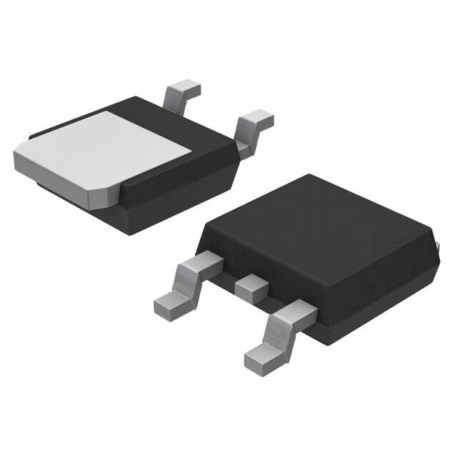
DPAK CASE 369C STYLE 2 D5003N A Y W = Device Code = Assembly Location = Year = Work Week 1 2 3 D5003N 1 = Gate 2 = Drain 3 = Source AYW
MOSFET MAXIMUM RATINGS (TJ = 25°C unless otherwise noted)
Rating Drain−to−Source Voltage Internally Clamped Gate−to−Source Voltage Drain Current Total Power Dissipation @ TA = 25°C (Note 1) @ TA = 25°C (Note 2) Thermal Resistance Junction−to−Case Junction−to−Ambient (Note 1) Junction−to−Ambient (Note 2) Single Pulse Drain−to−Source Avalanche Energy (VDD = 25 Vdc, VGS = 5.0 Vdc, IL = 3.2 Apk, L = 120 mH, RG = 25 W) Operating and Storage Temperature Range (Note 3) Continuous Symbol VDSS VGS ID PD Value 42 "14 Unit Vdc Vdc W
Internally Limited 1.3 2.3 3.0 95 54 600
RqJC RqJA RqJA EAS
°C/W
ORDERING INFORMATION
Device Package DPAK Shipping † 2500/Tape & Reel
mJ
NID5003NT4
TJ, Tstg
−55 to 150
°C
†For information on tape and reel specifications, including part orientation and tape sizes, please refer to our Tape and Reel Packaging Specification Brochure, BRD8011/D.
Preferred devices are recommended choices for future use and best overall value.
Stresses exceeding Maximum Ratings may damage the device. Maximum Ratings are stress ratings only. Functional operation above the Recommended Operating Conditions is not implied. Extended exposure to stresses above the Recommended Operating Conditions may affect device reliability. 1. Surface mounted onto minimum pad size (0.412″ square) FR4 PCB, 1 oz cu. 2. Mounted onto 1″ square pad size (1.127″ square) FR4 PCB, 1 oz cu. 3. Normal pre−fault operating range. See thermal limit range conditions.
© Semiconductor Components Industries, LLC, 2006
*Max current may be limited below this value depending on input conditions.
March, 2006− Rev. 3
1
Publication Order Number: NID5003N/D
�NID5003N
MOSFET ELECTRICAL CHARACTERISTICS (TJ = 25°C unless otherwise noted)
Characteristic OFF CHARACTERISTICS Drain−to−Source Clamped Breakdown Voltage (VGS = 0 Vdc, ID = 250 mAdc) (VGS = 0 Vdc, ID = 250 mAdc, TJ = −40°C to 150°C) Zero Gate Voltage Drain Current (VDS = 32 Vdc, VGS = 0 Vdc) (VDS = 32 Vdc, VGS = 0 Vdc, TJ = 150°C) Gate Input Current (VGS = 5.0 Vdc, VDS = 0 Vdc) ON CHARACTERISTICS Gate Threshold Voltage (VDS = VGS, ID = 1.2 mAdc) Threshold Temperature Coefficient Static Drain−to−Source On−Resistance (Note 4) (VGS = 10 Vdc, ID = 3.0 Adc, TJ @ 25°C) (VGS = 10 Vdc, ID = 3.0 Adc, TJ @ 150°C) Static Drain−to−Source On−Resistance (Note 4) (VGS = 5.0 Vdc, ID = 3.0 Adc, TJ @ 25°C) (VGS = 5.0 Vdc, ID = 3.0 Adc, TJ @ 150°C) Source−Drain Forward On Voltage (IS = 7.0 A, VGS = 0 V) SWITCHING CHARACTERISTICS Turn−on Time (Vin to 90% ID) Turn−off Time (Vin to 10% ID) Slew Rate On Slew Rate Off RL = 4.7 W, Vin = 0 to 10 V, VDD = 12 V RL = 4.7 W, Vin = 0 to 10 V, VDD = 12 V RL = 4.7 W, Vin = 0 to 10 V, VDD = 12 V RL = 4.7 W, Vin = 10 to 0 V, VDD = 12 V (VGS = 5.0 Vdc) VDS = 10 V (VGS = 5.0 Vdc, TJ = 150°C) (VGS = 10 Vdc) VDS = 10 V (VGS = 10 Vdc, TJ = 150°C) VGS = 5.0 Vdc VGS = 5.0 Vdc VGS = 10 Vdc VGS = 10 Vdc VDS = 35 V, (VGS = 5.0 V, Tj = 150°C) VDS = 35 V, (VGS = 10 V, Tj = 150°C) T(on) T(off) −dVDS/dton dVDS/dtoff ILIM ILIM TLIM(off) DTLIM(on) TLIM(off) DTLIM(on) Ig(fault) Ig(fault) − − − − 16 80 1.4 0.5 20 100 − − V/ms V/ms Adc ms VGS(th) 1.0 − − − − − − 1.7 5.0 42 76 50 88 0.95 2.2 − 51 104 58 125 1.1 Vdc −mV/°C mW V(BR)DSS 42 40 − − − 46 45 0.6 2.5 50 51 51 5.0 − 125 Vdc mAdc Symbol Min Typ Max Unit
IDSS
IGSSF
mAdc
RDS(on)
RDS(on)
mW
VSD
V
SELF PROTECTION CHARACTERISTICS (TJ = 25°C unless otherwise noted) (Note 5) Current Limit Current Limit Temperature Limit (Turn−off) Thermal Hysteresis Temperature Limit (Turn−off) Thermal Hysteresis Input Current during Thermal Fault Input Current during Thermal Fault 12 7 18 13 150 − 150 − 0.6 2.0 18 13 22 18 175 15 165 15 − − 24 18 30 25 200 − 185 − − − °C °C °C °C mA mA
ESD ELECTRICAL CHARACTERISTICS (TJ = 25°C unless otherwise noted) Electro−Static Discharge Capability Human Body Model (HBM) Machine Model (MM) ESD 4000 400 − − − − V
4. Pulse Test: Pulse Width ≤ 300 ms, Duty Cycle ≤ 2%. 5. Fault conditions are viewed as beyond the normal operating range of the part.
http://onsemi.com
2
�NID5003N
TYPICAL PERFORMANCE CURVES
35 ID, DRAIN CURRENT (AMPS) ID, DRAIN CURRENT (AMPS) 30 25 20 15 10 5 0 0 0.5 1 1.5 2 2.5 3 3.5 4 4.5 5 VDS, DRAIN−TO−SOURCE VOLTAGE (VOLTS) 25 VDS ≥ 10 V 20 15 10 5 0 25°C TJ = −55°C
100°C
1
3 1.5 2 3.5 2.5 VGS, GATE−TO−SOURCE VOLTAGE (VOLTS)
4
Figure 1. On−Region Characteristics
RDS(on), DRAIN−TO−SOURCE RESISTANCE (W) RDS(on), DRAIN−TO−SOURCE RESISTANCE (W) 1.0 0.9 0.8 0.7 0.6 0.5 0.4 0.3 0.2 0.1 0 2 5 7 8 9 4 6 VGS, GATE−TO−SOURCE VOLTAGE (VOLTS) 3 10 0.06 0.055 0.05 0.045 0.04 0.035 0.03
Figure 2. Transfer Characteristics
ID = 5 A TJ = 25°C
TJ = 25°C VGS = 5 V
VGS = 10 V
2
3
4
5
6
7
8
9
10
ID, DRAIN CURRENT (AMPS)
Figure 3. On−Resistance vs. Gate−to−Source Voltage
1.8 RDS(on), DRAIN−TO−SOURCE RESISTANCE (NORMALIZED) 1.6 1.4 1.2 1.0 0.8 0.6 0.4 0.2 0 −50 −30 −10 10 30 50 70 90 110 130 150 10 100000
Figure 4. On−Resistance vs. Drain Current and Gate Voltage
ID = 5 A VGS = 10 V
VGS = 0 V IDSS, LEAKAGE (nA) 10000 TJ = 150°C
1000
TJ = 100°C
100
0
5
10
15
20
25
30
35
40
45
TJ, JUNCTION TEMPERATURE (°C)
VDS, DRAIN−TO−SOURCE VOLTAGE (VOLTS)
Figure 5. On−Resistance Variation with Temperature
Figure 6. Drain−to−Source Leakage Current vs. Voltage
http://onsemi.com
3
�NID5003N
TYPICAL PERFORMANCE CURVES
10 IS, SOURCE CURRENT (AMPS) VGS = 0 V TJ = 25°C
1
0.1 0.4
0.5
0.6
0.7
0.8
0.9
1
VSD, SOURCE−TO−DRAIN VOLTAGE (VOLTS)
Figure 7. Diode Forward Voltage vs. Current
http://onsemi.com
4
�NID5003N
PACKAGE DIMENSIONS
DPAK CASE 369C−01 ISSUE O
−T− B V R
4 SEATING PLANE INCHES MIN MAX 0.235 0.245 0.250 0.265 0.086 0.094 0.027 0.035 0.018 0.023 0.037 0.045 0.180 BSC 0.034 0.040 0.018 0.023 0.102 0.114 0.090 BSC 0.180 0.215 0.025 0.040 0.020 −−− 0.035 0.050 0.155 −−− MILLIMETERS MIN MAX 5.97 6.22 6.35 6.73 2.19 2.38 0.69 0.88 0.46 0.58 0.94 1.14 4.58 BSC 0.87 1.01 0.46 0.58 2.60 2.89 2.29 BSC 4.57 5.45 0.63 1.01 0.51 −−− 0.89 1.27 3.93 −−−
C E
S
A
1 2 3
Z U
K F L D G
2 PL
J H 0.13 (0.005)
M
DIM A B C D E F G H J K L R S U V Z
T
STYLE 2: PIN 1. GATE 2. DRAIN 3. SOURCE 4. DRAIN
SOLDERING FOOTPRINT
6.20 0.244 2.58 0.101 5.80 0.228 1.6 0.063 6.172 0.243 3.0 0.118
SCALE 3:1
mm inches
http://onsemi.com
5
�NID5003N
HDPlus is a trademark of Semiconductor Components Industries, LLC (SCILLC)
ON Semiconductor and are registered trademarks of Semiconductor Components Industries, LLC (SCILLC). SCILLC reserves the right to make changes without further notice to any products herein. SCILLC makes no warranty, representation or guarantee regarding the suitability of its products for any particular purpose, nor does SCILLC assume any liability arising out of the application or use of any product or circuit, and specifically disclaims any and all liability, including without limitation special, consequential or incidental damages. “Typical” parameters which may be provided in SCILLC data sheets and/or specifications can and do vary in different applications and actual performance may vary over time. All operating parameters, including “Typicals” must be validated for each customer application by customer’s technical experts. SCILLC does not convey any license under its patent rights nor the rights of others. SCILLC products are not designed, intended, or authorized for use as components in systems intended for surgical implant into the body, or other applications intended to support or sustain life, or for any other application in which the failure of the SCILLC product could create a situation where personal injury or death may occur. Should Buyer purchase or use SCILLC products for any such unintended or unauthorized application, Buyer shall indemnify and hold SCILLC and its officers, employees, subsidiaries, affiliates, and distributors harmless against all claims, costs, damages, and expenses, and reasonable attorney fees arising out of, directly or indirectly, any claim of personal injury or death associated with such unintended or unauthorized use, even if such claim alleges that SCILLC was negligent regarding the design or manufacture of the part. SCILLC is an Equal Opportunity/Affirmative Action Employer. This literature is subject to all applicable copyright laws and is not for resale in any manner.
PUBLICATION ORDERING INFORMATION
LITERATURE FULFILLMENT: N. American Technical Support: 800−282−9855 Toll Free Literature Distribution Center for ON Semiconductor USA/Canada P.O. Box 61312, Phoenix, Arizona 85082−1312 USA Phone: 480−829−7710 or 800−344−3860 Toll Free USA/Canada Japan : ON Semiconductor, Japan Customer Focus Center 2−9−1 Kamimeguro, Meguro−ku, Tokyo, Japan 153−0051 Fax: 480−829−7709 or 800−344−3867 Toll Free USA/Canada Phone: 81−3−5773−3850 Email: orderlit@onsemi.com ON Semiconductor Website: http://onsemi.com Order Literature: http://www.onsemi.com/litorder For additional information, please contact your local Sales Representative.
http://onsemi.com
6
NID5003N/D
�