NJW44H11G
80 V NPN, 10 A
Power Transistor
These series of plastic, silicon NPN power transistors can be used as
general purpose power amplification and switching such as output or
driver stages in applications such as switching regulators, converters
and power amplifiers.
Features
• Fast Switching Speeds
• High Frequency
• These Devices are Pb−Free, Halogen Free/BFR Free and are RoHS
http://onsemi.com
80 VOLT, 10 AMPS
NPN POWER TRANSISTORS
Compliant
NPN
COLLECTOR 2, 4
Benefits
•
•
•
•
•
Reliable Performance at Higher Powers
Symmetrical Characteristics in Complementary Configurations
Accurate Reproduction of Input Signal
Greater Dynamic Range
High Amplifier Bandwidth
1
BASE
EMITTER 3
Applications
• High−end Consumer Audio Products
♦
♦
MARKING
DIAGRAM
4
Home Amplifiers
Home Receivers
NJWxxxG
AYWW
MAXIMUM RATINGS (TA = 25°C)
Rating
Symbol
Max
Unit
Collector−Emitter Voltage
VCEO
80
Vdc
Emitter−Base Voltage
VEBO
5.0
Vdc
IC
10
A
Collector Current − Peak (Note 1)
ICM
20
A
Total Power Dissipation @ TC = 25°C
PD
120
Watts
Characteristic
Symbol
Max
Unit
Thermal Resistance, Junction to Case
RqJC
1.04
°C/W
TJ, Tstg
− 65 to
+150
°C
Collector Current − Continuous
THERMAL CHARACTERISTICS
Junction and Storage Temperature
Range
Stresses exceeding Maximum Ratings may damage the device. Maximum
Ratings are stress ratings only. Functional operation above the Recommended
Operating Conditions is not implied. Extended exposure to stresses above the
Recommended Operating Conditions may affect device reliability.
1. Pulse Test: Pulse Width = 5 ms, Duty Cycle ≤ 10%.
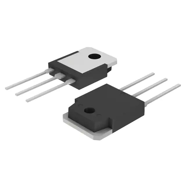
TO−3P
PLASTIC
CASE 340AB
1
2
3
xxx
G
A
Y
WW
1
2
3
= TBD
= Pb−Free Package
= Assembly Location
= Year
= Work Week
ORDERING INFORMATION
Device
NJW44H11G
Package
Shipping
TO−3P
(Pb−Free)
30 Units/Rail
*For additional information on our Pb−Free strategy and soldering details, please
download the ON Semiconductor Soldering and Mounting Techniques
Reference Manual, SOLDERRM/D.
© Semiconductor Components Industries, LLC, 2013
September, 2013 − Rev. 0
1
Publication Order Number:
NJW44H11/D
�NJW44H11G
ELECTRICAL CHARACTERISTICS (TA = 25°C unless otherwise noted)
Symbol
Min
Typ
Max
Unit
Collector−Emitter Sustaining Voltage
(IC = 30 mAdc, IB = 0)
VCEO
80
−
−
Vdc
Collector−Cutoff Current
(VCE = Rated VCEO, VBE = 0)
ICES
−
−
10
mAdc
Emitter Cutoff Current
(VBE = 5.0 Vdc)
IEBO
−
−
10
mAdc
100
80
−
−
400
320
Characteristic
OFF CHARACTERISTICS
ON CHARACTERISTICS
hFE
DC Current Gain
(IC = 2 A, VCE = 2 V)
(IC = 4 A, VCE = 2 V)
−
Collector−Emitter Saturation Voltage
(IC = 8 A, IB = 400 mA)
VCE(sat)
−
−
1.0
V
Base−Emitter Turn−on Voltage
(IC = 8 A, VCE = 2.0 V)
VBE(on)
−
−
1.5
V
Cobo
−
65
−
pF
fT
−
85
−
MHz
td + tr
−
300
−
ns
Storage Time
(IC = 5.0 Adc, IB1 = IB2 = 0.5 A)
ts
−
500
−
ns
Fall Time
(IC = 5.0 Adc, IB1 = IB2 = 0.5 A)
tf
−
140
−
ns
DYNAMIC CHARACTERISTICS
Output Capacitance
(VCB = 10 V, f = 1.0 MHz)
Cutoff Frequency
(IC = 500 mA, VCE = 5 V, f = 1.0 MHz)
SWITCHING TIMES
Delay and Rise Times
(IC = 5.0 Adc, IB1 = 0.5 A)
http://onsemi.com
2
�NJW44H11G
TYPICAL CHARACTERISTICS
500
500
450
150°C
400
350
hFE, DC CURRENT GAIN
hFE, DC CURRENT GAIN
450
25°C
300
250
200
−55°C
150
100
50
0
0.01
0.1
1
10
250
−55°C
200
150
100
VCE = 4 V
0.01
0.1
1
10
IC, COLLECTOR CURRENT (A)
Figure 1. DC Current Gain
Figure 2. DC Current Gain
VCE(sat) @ IC/IB = 10
COLLECTOR−EMITTER
SATURATION VOLTAGE (V)
COLLECTOR−EMITTER
SATURATION VOLTAGE (V)
150°C
0.30
0.25
25°C
0.20
0.15
0.10
−55°C
0.05
0.01
0.1
1
VCE(sat) @ IC/IB = 20
0.35
150°C
0.30
0.25
25°C
0.20
0.15
0.10
−55°C
0.05
0
10
0.01
0.1
1
10
IC, COLLECTOR CURRENT (A)
IC, COLLECTOR CURRENT (A)
Figure 3. Collector Emitter Saturation Voltage
Figure 4. Collector Emitter Saturation Voltage
1.2
1.2
1.0
BASE−EMITTER VOLTAGE (V)
BASE−EMITTER SATURATION VOLTAGE (V)
25°C
300
0.40
0.35
−55°C
0.8
25°C
0.6
150°C
0.4
0.2
0
350
IC, COLLECTOR CURRENT (A)
0.40
0
400
50
0
VCE = 2 V
150°C
VBE(sat) @ IC/IB = 10
0.01
0.1
1
1.0
25°C
0.6
150°C
0.4
0.2
0
10
−55°C
0.8
VBE(on) @ VCE = 4 V
0.01
0.1
1
IC, COLLECTOR CURRENT (A)
IC, COLLECTOR CURRENT (A)
Figure 5. Base Emitter Saturation Voltage
Figure 6. Base Emitter “ON” Voltage
http://onsemi.com
3
10
�NJW44H11G
TYPICAL CHARACTERISTICS
90
80
TJ = 25°C
f = 1 MHz
200
fT, CURRENT BANDWIDTH
PRODUCT (MHz)
Cob, OUTPUT CAPACITANCE (pF)
250
150
100
50
60
50
40
VCE = 5 V
ftest = 1 MHz
TJ = 25°C
30
20
10
0
0
10
20
30
40
50
60
70
0
80
0.1
1
10
IC, COLLECTOR CURRENT (A)
Figure 7. Output Capacitance
Figure 8. Current Gain Bandwidth Product
100
IC, COLLECTOR CURRENT (A)
120
100
80
60
40
20
0
0.01
VCB, COLLECTOR−BASE VOLTAGE
140
PD, POWER DISSIPATION (W)
70
0
20
40
60
80
100
120
140
10
1 mS
10 mS
1
0.1
0.01
160
1 Sec
1
10
T, TEMPERATURE (°C)
VCE, COLLECTOR−EMITTER VOLTAGE (V)
Figure 9. Power Temperature Derating
Figure 10. Safe Operating Area (SOA)
http://onsemi.com
4
100
�MECHANICAL CASE OUTLINE
PACKAGE DIMENSIONS
TO−3P−3LD
CASE 340AB−01
ISSUE A
B
A
B
C
Q
4
DATE 30 OCT 2007
SEATING
PLANE
U
E
SCALE 1:1
A
L
(3°)
P
K
1
2
3
3X
D
0.25
G
NOTES:
1. DIMENSIONING AND TOLERANCING PER ASME
Y14.5M, 1994.
2. CONTROLLING DIMENSION: MILLIMETERS
3. DIMENSION b APPLIES TO PLATED TERMINAL
AND IS MEASURED BETWEEN 0.15 AND 0.30mm
FROM THE TERMINAL TIP.
4. DIMENSION A AND B DO NOT INCLUDE MOLD
FLASH, PROTRUSIONS, OR GATE BURRS.
M
A B
S
H
J
G
F
W
DIM
A
B
C
D
E
F
G
H
J
K
L
P
Q
U
W
MILLIMETERS
MIN
NOM
MAX
19.70
19.90
20.10
15.40
15.60
15.80
4.60
4.80
5.00
0.80
1.00
1.20
1.45
1.50
1.65
1.80
2.00
2.20
5.45 BSC
1.20
1.40
1.60
0.55
0.60
0.75
19.80
20.00
20.20
18.50
18.70
18.90
3.30
3.50
3.70
3.10
3.20
3.50
5.00 REF
2.80
3.00
3.20
GENERIC MARKING
DIAGRAM*
STYLE 1:
PIN 1. BASE
2. COLLECTOR
3. EMITTER
4. COLLECTOR
STYLE 2:
PIN 1. ANODE
2. CATHODE
3. ANODE
4. CATHODE
STYLE 3:
PIN 1. GATE
2. DRAIN
3. SOURCE
4. DRAIN
xxxxxG
AYWW
xxxxx
G
A
Y
WW
= Specific Device Code
= Pb−Free Package
= Assembly Location
= Year
= Work Week
*This information is generic. Please refer
to device data sheet for actual part
marking. Pb−Free indicator, “G”, may
or not be present.
DOCUMENT NUMBER:
DESCRIPTION:
98AON25095D
TO−3P−3LD
Electronic versions are uncontrolled except when accessed directly from the Document Repository.
Printed versions are uncontrolled except when stamped “CONTROLLED COPY” in red.
PAGE 1 OF 1
ON Semiconductor and
are trademarks of Semiconductor Components Industries, LLC dba ON Semiconductor or its subsidiaries in the United States and/or other countries.
ON Semiconductor reserves the right to make changes without further notice to any products herein. ON Semiconductor makes no warranty, representation or guarantee regarding
the suitability of its products for any particular purpose, nor does ON Semiconductor assume any liability arising out of the application or use of any product or circuit, and specifically
disclaims any and all liability, including without limitation special, consequential or incidental damages. ON Semiconductor does not convey any license under its patent rights nor the
rights of others.
© Semiconductor Components Industries, LLC, 2019
www.onsemi.com
�onsemi,
, and other names, marks, and brands are registered and/or common law trademarks of Semiconductor Components Industries, LLC dba “onsemi” or its affiliates
and/or subsidiaries in the United States and/or other countries. onsemi owns the rights to a number of patents, trademarks, copyrights, trade secrets, and other intellectual property.
A listing of onsemi’s product/patent coverage may be accessed at www.onsemi.com/site/pdf/Patent−Marking.pdf. onsemi reserves the right to make changes at any time to any
products or information herein, without notice. The information herein is provided “as−is” and onsemi makes no warranty, representation or guarantee regarding the accuracy of the
information, product features, availability, functionality, or suitability of its products for any particular purpose, nor does onsemi assume any liability arising out of the application or use
of any product or circuit, and specifically disclaims any and all liability, including without limitation special, consequential or incidental damages. Buyer is responsible for its products
and applications using onsemi products, including compliance with all laws, regulations and safety requirements or standards, regardless of any support or applications information
provided by onsemi. “Typical” parameters which may be provided in onsemi data sheets and/or specifications can and do vary in different applications and actual performance may
vary over time. All operating parameters, including “Typicals” must be validated for each customer application by customer’s technical experts. onsemi does not convey any license
under any of its intellectual property rights nor the rights of others. onsemi products are not designed, intended, or authorized for use as a critical component in life support systems
or any FDA Class 3 medical devices or medical devices with a same or similar classification in a foreign jurisdiction or any devices intended for implantation in the human body. Should
Buyer purchase or use onsemi products for any such unintended or unauthorized application, Buyer shall indemnify and hold onsemi and its officers, employees, subsidiaries, affiliates,
and distributors harmless against all claims, costs, damages, and expenses, and reasonable attorney fees arising out of, directly or indirectly, any claim of personal injury or death
associated with such unintended or unauthorized use, even if such claim alleges that onsemi was negligent regarding the design or manufacture of the part. onsemi is an Equal
Opportunity/Affirmative Action Employer. This literature is subject to all applicable copyright laws and is not for resale in any manner.
PUBLICATION ORDERING INFORMATION
LITERATURE FULFILLMENT:
Email Requests to: orderlit@onsemi.com
onsemi Website: www.onsemi.com
◊
TECHNICAL SUPPORT
North American Technical Support:
Voice Mail: 1 800−282−9855 Toll Free USA/Canada
Phone: 011 421 33 790 2910
Europe, Middle East and Africa Technical Support:
Phone: 00421 33 790 2910
For additional information, please contact your local Sales Representative
�