NLAS4685
Ultra−Low Resistance
Dual SPDT Analog Switch
The NLAS4685 is an advanced CMOS analog switch fabricated in
Sub−micron silicon gate CMOS technology. The device is a dual
Independent Single Pole Double Throw (SPDT) switch featuring
Ultra−Low RON of 0.8 �, for the Normally Closed (NC) switch and
for the Normally Opened switch (NO) at 2.7 V.
The part also features guaranteed Break Before Make switching,
assuring the switches never short the driver.
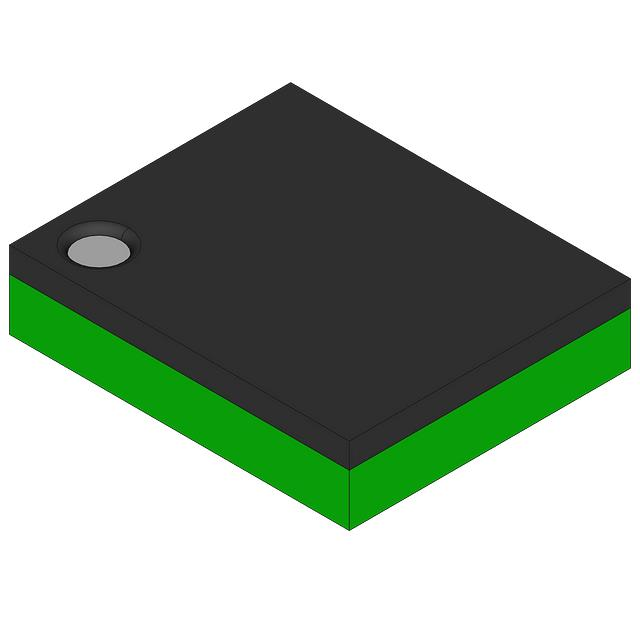
The NLAS4685 is available in a 2.0 x 1.5 mm bumped die array,
with a 3 x 4 arrangement of solder bumps. The pitch of the solder
bumps is 0.5 mm for easy handling.
Features
XXD
A1
A1
XX = Device Code
D
= Date Code
VCC = 2.7−3.3 V
Single Supply Operation from 1.8−5.5 V
Tiny 2 x 1.5 mm Bumped Die
Low Crosstalk, t 81 dB at 100 kHz
Full 0−VCC Signal Handling Capability
High Isolation, −65 dB at 100 kHz
Low Standby Current, t50 nA
Low Distortion, t0.14% THD
RON Flatness of 0.15 �
Pin for Pin Replacement for MAX4685
Pb−Free Package is Available
PIN CONNECTIONS AND LOGIC DIAGRAM
(Top View)
GND
B1
Applications
•
•
•
•
•
MARKING
DIAGRAM
Microbump−10
CASE 489AA
• Ultra−Low RON, t0.8 � at 2.7 V
• Threshold Adjusted to Function with 1.8 V Control at
•
•
•
•
•
•
•
•
•
•
http://onsemi.com
NC1
C1
A1
NC2
IN1
C2
A2
IN2
COM1
C3
A3
COM2
NO1
C4
A4
NO2
B4
Cell Phone
Speaker Switching
Power Switching (Up to 100 mA)
Modems
Automotive
VCC
FUNCTION TABLE
IN 1, 2
NO 1, 2
NC 1, 2
0
1
OFF
ON
ON
OFF
ORDERING INFORMATION
Package
Shipping †
NLAS4685FCT1
Microbump
3000 Tape/Reel
NLAS4685FCT1G
Microbump
(Pb−Free)
3000 Tape/Reel
Device
†For information on tape and reel specifications,
including part orientation and tape sizes, please
refer to our Tape and Reel Packaging Specification
Brochure, BRD8011/D.
© Semiconductor Components Industries, LLC, 2005
August, 2005 − Rev. 2
1
Publication Order Number:
NLAS4685/D
�NLAS4685
MAXIMUM RATINGS
Symbol
Parameter
VCC
Positive DC Supply Voltage
VIS
Analog Input Voltage (VNO, VNC, or VCOM) (Note 1)
VIN
Digital Select Input Voltage
IIK
DC Current, Into or Out of Any Pin
Value
Unit
*0.5 to )7.0
V
*0.5 v VIS v VCC )0.5
V
*0.5 v VI v)7.0
V
$50
mA
Maximum ratings are those values beyond which device damage can occur. Maximum ratings applied to the device are individual stress limit
values (not normal operating conditions) and are not valid simultaneously. If these limits are exceeded, device functional operation is not implied,
damage may occur and reliability may be affected.
1. Signal voltage on NC, NO, and COM exceeding VCC or GND are clamped by the internal diodes. Limit forward diode current to maximum
current rating.
RECOMMENDED OPERATING CONDITIONS
Symbol
Parameter
Min
Max
Unit
1.8
5.5
V
5.5
V
VCC
DC Supply Voltage
VIN
Digital Select Input Voltage
GND
VIS
Analog Input Voltage (NC, NO, COM)
GND
VCC
V
TA
Operating Temperature Range
*55
)125
°C
tr, tf
Input Rise or Fall Time, SELECT
0
0
100
20
ns/V
VCC = 3.3 V $ 0.3 V
VCC = 5.0 V $ 0.5 V
DC CHARACTERISTICS − Digital Section (Voltages Referenced to GND)
Guaranteed Limit
Symbol
Parameter
Condition
VCC $10%
*555C to 255C
t855C
t1255C
Unit
VIH
Minimum High−Level Input
Voltage, Select Inputs
2.0
2.5
3.0
5.0
1.4
1.4
1.4
2.0
1.4
1.4
1.4
2.0
1.4
1.4
1.4
2.0
V
VIL
Maximum Low−Level Input
Voltage, Select Inputs
2.0
2.5
3.0
5.0
0.5
0.5
0.5
0.8
0.5
0.5
0.5
0.8
0.5
0.5
0.5
0.8
V
IIN
Maximum Input Leakage
Current, Select Inputs
VIN = 5.5 V or GND
5.5
$ 1.0
$ 1.0
$ 1.0
�A
IOFF
Power Off Leakage Current
VIN = 5.5 V or GND
0
$10
$10
$10
�A
ICC
Maximum Quiescent Supply
Current
Select and VIS = VCC or GND
5.5
$ 180
$ 200
$ 200
nA
http://onsemi.com
2
�NLAS4685
DC ELECTRICAL CHARACTERISTICS − Analog Section
Guaranteed Maximum Limit
−555C to 255C
Symbol
VCC $10%
Min
Max
t855C
Max
Unit
2.0
0.8
0.8
2.0
1.0
0.9
�
0.35
0.35
0.35
0.35
0.35
0.35
0.35
0.35
0.35
�
2.5
0.18
0.18
0.18
�
3.0
0.06
0.06
0.06
5.0
0.06
0.06
0.06
Parameter
Condition
RON
(NC, NO)
“ON” Resistance
(Note 2)
VIN w VIH
VIS = GND to VCC
IINI v 100 mA
2.5
3.0
5.0
2.0
0.8
0.8
RFLAT
(NC, NO)
On−Resistance
Flatness (Notes 2, 4)
ICOM = 100 mA
VIS = 0 to VCC
2.5
3.0
5.0
�RON
On−Resistance Match
Between Channels
(Notes 2 and 3)
VIS = 1.3 V;
ICOM = 100 mA
VIS = 1.5 V;
ICOM = 100 mA
VIS = 2.8 V;
ICOM = 100 mA
Min
Max
t1255C
Min
INC(OFF)
INO(OFF)
NC or NO Off
Leakage Current
(Figure 10)
VIN = VIL or VIH
VNO or VNC = 1.0
VCOM = 4.5 V
5.5
−1
1
−10
10
−150
150
nA
ICOM(ON)
COM ON
Leakage Current
(Figure 10)
VIN = VIL or VIH
VNO 1.0 V or 4.5 V with
VNC floating or
VNC 1.0 V or 4.5 V with
VNO floating
VCOM = 1.0 V or 4.5 V
5.5
−1
1
−10
10
−150
150
nA
2. Guaranteed by design. Resistance measurements do not include test circuit or package resistance.
3. �RON = RON(MAX) − RON(MIN) between all switches.
4. Flatness is defined as the difference between the maximum and minimum value of on−resistance as measured over the specified analog
signal ranges.
http://onsemi.com
3
�NLAS4685
AC ELECTRICAL CHARACTERISTICS (Input tr = tf = 3.0 ns)
Guaranteed Maximum Limit
Symbol
Parameter
Test Conditions
VCC
(V)
VIS
(V)
*555C to 255C
Min
Typ*
t855C
Max
Min
Max
t1255C
Min
Max
Unit
tON
Turn−On Time
RL = 50 �� CL = 35 pF
(Figures 2 and 3)
2.5
3.0
5.0
1.3
1.5
2.8
55
50
30
65
60
35
70
60
35
ns
tOFF
Turn−Off Time
RL = 50 �� CL = 35 pF
(Figures 2 and 3)
2.5
3.0
5.0
1.3
1.5
2.8
55
50
25
65
60
30
70
60
30
ns
tBBM
Minimum Break−Before−Make
Time
VIS = 3.0
RL = 300 �� CL = 35 pF
(Figure 1)
3.0
1.5
ns
2
15
Typical @ 25, VCC = 5.0 V
CNC Off
CNO Off
CNC On
CNO On
VCC = 3.0 V
NC Off Capacitance, f = 1 MHz
NO Off Capacitance, f = 1 MHz
NC On Capacitance, f = 1 MHz
NO On Capacitance, f = 1 MHz
208
102
547
431
pF
*Typical Characteristics are at 25°C.
ADDITIONAL APPLICATION CHARACTERISTICS (Voltages Referenced to GND Unless Noted) (Note 6)
Symbol
Parameter
VCC
V
Condition
Typical
255C
Unit
3.0
11.5
MHz
BW
Maximum On−Channel −3dB
Bandwidth or Minimum Frequency
Response
VIN = 0 dBm
VIN centered between VCC and GND
(Figure 4)
VONL
Maximum Feed−through On Loss
VIN = 0 dBm @ 100 kHz to 50 MHz
VIN centered between VCC and GND (Figure 4)
3.0
−0.05
dB
f = 100 kHz; VIS = 1 V RMS; CL = 5 nF
VIN centered between VCC and GND(Figure 4)
3.0
−65
dB
VISO
Off−Channel Isolation
NC/NO
Q
Charge Injection Select Input to
Common I/O
VIN = VCC to GND, RIS = 0 �, CL = 1 nF
Q = CL − �VOUT (Figure 5)
3.0
5.0
15
20
pC
THD
Total Harmonic Distortion
THD + Noise
FIS = 20 Hz to 20 kHz, RL = Rgen = 600 �, CL = 50 pF
VIS = 1 V RMS
3.0
0.14
%
VCT
Channel−to−Channel Crosstalk
f = 100 kHz; VIS = 1 V RMS, CL = 5 pF, RL = 50 �
VIN centered between VCC and GND (Figure 4)
3.0
−81
dB
5. Off−Channel Isolation = 20log10 (Vcom/Vno), Vcom = output, Vno = input to off switch.
6. −40°C specifications are guaranteed by design.
http://onsemi.com
4
�NLAS4685
VCC
DUT
VCC
Input
Output
GND
VOUT
0.1 �F
50 �
tBMM
35 pF
90%
90% of VOH
Output
Switch Select Pin
GND
Figure 1. tBBM (Time Break−Before−Make)
VCC
Input
DUT
VCC
0.1 �F
50%
Output
VOUT
Open
50%
0V
50 �
VOH
90%
35 pF
90%
Output
VOL
Input
tON
tOFF
Figure 2. tON/tOFF
VCC
VCC
Input
DUT
Output
50 �
50%
VOUT
Open
50%
0V
VOH
35 pF
Output
10%
VOL
Input
tOFF
Figure 3. tON/tOFF
http://onsemi.com
5
10%
tON
�NLAS4685
50 �
DUT
Reference
Transmitted
Input
Output
50 � Generator
50 �
Channel switch control/s test socket is normalized. Off isolation is measured across an off channel. On loss is
the bandwidth of an On switch. VISO, Bandwidth and VONL are independent of the input signal direction.
ǒVVOUT
Ǔ for VIN at 100 kHz
IN
VOUT
Ǔ for VIN at 100 kHz to 50 MHz
VONL = On Channel Loss = 20 Log ǒ
VIN
VISO = Off Channel Isolation = 20 Log
Bandwidth (BW) = the frequency 3 dB below VONL
VCT = Use VISO setup and test to all other switch analog input/outputs terminated with 50 �
Figure 4. Off Channel Isolation/On Channel Loss (BW)/Crosstalk
(On Channel to Off Channel)/VONL
DUT
VCC
VIN
Output
Open
GND
CL
Output
Off
VIN
Figure 5. Charge Injection: (Q)
http://onsemi.com
6
On
Off
�VOUT
�NLAS4685
10
1.6
Vin THRESHOLD (V)
1.4
THD (%)
1
1,NC1
0.1
1, NO1
Threshold Rising
1.2
1
Threshold Falling
0.8
0.6
0.4
0.2
0.01
0
1
10
100
1000
10000
0
100000
4
6
FREQUENCY (Hz)
VCC (V)
Figure 6. Total Harmonic Distortion Plus Noise
versus Frequency
Figure 7. Voltage in Threshold on Logic Pins
70
200
1, NO1
60
T−on 2.5V
−200
T−on / T−off (ns)
0
1,NC1
−400
T−off 2.5 V
50
T−on 3.0 V
40
T−off 3.0 VT−off 5 V
30
20
T−on 5 V
−600
−800
10
Q (pC),
VCC = 5 V
0
2
4
0
−55
6
−30
−5
20
45
70
95
120
Vin (V)
TEMPERATURE (°C)
Figure 8. Charge Injection versus Vis
Figure 9. T−on/T−off Time versus Temperature
1000
NO/NC CURRENT LEAKAGE (nA)
Charge Injection “Q’’ (pC)
2
2.75 V
100
10
Comm / Closed Switch
1
0.1
Open Switch
0.01
0.001
−55
−5
45
95
TEMPERATURE (°C)
Figure 10. NO/NC Current Leakage Off and On,
VCC = 5 V
http://onsemi.com
7
�NLAS4685
1.3
100
1.1
TA = +25°C
ICOM = 100 mA
+85°C
5.5 V
+25°C
0.9
10
RON (�)
ICC CuRRENT (nA)
1000
1
0.7
0.1
0.5
0.01
0.3
0.001
−40°C
0.1
−55
−5
45
95
0.0
1.0
2.0
TEMPERATURE (°C)
3.0
4.0
5.0
VCOM (V)
Figure 11. ICC Current Leakage versus
Temperature VCC = 5.5 V
Figure 12. NC/NO On−Resistance versus
COM Voltage
4.5
1.8 V
TA = +25°C
ICOM = 100 mA
4
3.5
2.0 V
RON (�)
3
2.5
2.7 V
2.3 V
2
2.5 V
1.5
3.0 V
5.0 V
1
0.5
0
0.0
1.0
2.0
3.0
4.0
5.0
VCOM (V)
Figure 13. NC/NO On−Resistance versus
COM Voltage
0
BANDWIDTH (dB/Div)
−1
10
0
Phase Shift
(Degrees)
0
PHASE (Degrees)
Bandwidth (On − Loss)
−1
Off−Isolation
−10
Crosstalk
VCC = 3.0 V
TA = 25°C
−10
0.001
0.01
VCC = 3.0 V
TA = 25°C
0.1
1.0
10
−10
0.001
100
FREQUENCY (MHz)
0.01
0.1
1.0
10
100
FREQUENCY (MHz)
Figure 14. NC/NO Bandwidth and Phase Shift
versus Frequency
Figure 15. NC/NO Off Isolation and Crosstalk
http://onsemi.com
8
�NLAS4685
0.9
100
+85°C
0.8
+25°C
AVERAGE RON (�)
60
T−on
40
T−off
0.7
0.6
0.4
0.3
0.2
0
1.8
−40°C
0.5
20
VCC = 5 V
ICOM = 100 mA
0.1
2.8
3.8
0.0
4.8
1.0
VCC (V)
2.0
0.9
+85°C +25°C
0.7
−40°C
0.6
0.5
0.4
0.3
0.1
4.0
Figure 17. NC/NO On−Resistance versus
COM Voltage
0.8
0.2
3.0
VCOM (V)
Figure 16. T−on/T−off versus VCC
AVERAGE RON (�)
T−on / T−off (ns)
80
VCC = 3 V
ICOM = 100 mA
0.0
1.0
2.0
VCOM (V)
Figure 18. NC/NO On−Resistance versus
COM Voltage
http://onsemi.com
9
3.0
5.0
�MECHANICAL CASE OUTLINE
PACKAGE DIMENSIONS
10 PIN FLIP−CHIP
CASE 489AA−01
ISSUE A
DATE 04 MAY 2004
1
NOTES:
1. DIMENSIONING AND TOLERANCING
PER ASME Y14.5M, 1994.
2. CONTROLLING DIMENSION:
MILLIMETERS.
3. COPLANARITY APPLIES TO SPHERICAL
CROWNS OF SOLDER BALLS.
SCALE 4:1
D
4X
A
B
0.10 C
MILLIMETERS
DIM MIN
MAX
A
−−− 0.650
A1 0.210 0.270
A2 0.280 0.380
D
1.965 BSC
E
1.465 BSC
b
0.250 0.350
e
0.500 BSC
D1
1.500 BSC
1.000 BSC
E1
E
PIN ONE
CORNER
A1
0.10 C
A2
GENERIC
MARKING DIAGRAM*
A
0.075 C
C
SEATING
PLANE
xxxx
YYWW
D1
A1
e
10 X
b
0.15 C A B
0.05 C
C
E1
B
xxxx
YY
WW
= Specific Device Code
= Year
= Work Week
A
DOCUMENT NUMBER:
DESCRIPTION:
1
2
3
4
e
98AON12946D
10 PIN FLIP−CHIP
*This information is generic. Please refer to
device data sheet for actual part marking.
Pb−Free indicator, “G” or microdot “ G”,
may or may not be present.
Electronic versions are uncontrolled except when accessed directly from the Document Repository.
Printed versions are uncontrolled except when stamped “CONTROLLED COPY” in red.
PAGE 1 OF 1
ON Semiconductor and
are trademarks of Semiconductor Components Industries, LLC dba ON Semiconductor or its subsidiaries in the United States and/or other countries.
ON Semiconductor reserves the right to make changes without further notice to any products herein. ON Semiconductor makes no warranty, representation or guarantee regarding
the suitability of its products for any particular purpose, nor does ON Semiconductor assume any liability arising out of the application or use of any product or circuit, and specifically
disclaims any and all liability, including without limitation special, consequential or incidental damages. ON Semiconductor does not convey any license under its patent rights nor the
rights of others.
© Semiconductor Components Industries, LLC, 2019
www.onsemi.com
�onsemi,
, and other names, marks, and brands are registered and/or common law trademarks of Semiconductor Components Industries, LLC dba “onsemi” or its affiliates
and/or subsidiaries in the United States and/or other countries. onsemi owns the rights to a number of patents, trademarks, copyrights, trade secrets, and other intellectual property.
A listing of onsemi’s product/patent coverage may be accessed at www.onsemi.com/site/pdf/Patent−Marking.pdf. onsemi reserves the right to make changes at any time to any
products or information herein, without notice. The information herein is provided “as−is” and onsemi makes no warranty, representation or guarantee regarding the accuracy of the
information, product features, availability, functionality, or suitability of its products for any particular purpose, nor does onsemi assume any liability arising out of the application or use
of any product or circuit, and specifically disclaims any and all liability, including without limitation special, consequential or incidental damages. Buyer is responsible for its products
and applications using onsemi products, including compliance with all laws, regulations and safety requirements or standards, regardless of any support or applications information
provided by onsemi. “Typical” parameters which may be provided in onsemi data sheets and/or specifications can and do vary in different applications and actual performance may
vary over time. All operating parameters, including “Typicals” must be validated for each customer application by customer’s technical experts. onsemi does not convey any license
under any of its intellectual property rights nor the rights of others. onsemi products are not designed, intended, or authorized for use as a critical component in life support systems
or any FDA Class 3 medical devices or medical devices with a same or similar classification in a foreign jurisdiction or any devices intended for implantation in the human body. Should
Buyer purchase or use onsemi products for any such unintended or unauthorized application, Buyer shall indemnify and hold onsemi and its officers, employees, subsidiaries, affiliates,
and distributors harmless against all claims, costs, damages, and expenses, and reasonable attorney fees arising out of, directly or indirectly, any claim of personal injury or death
associated with such unintended or unauthorized use, even if such claim alleges that onsemi was negligent regarding the design or manufacture of the part. onsemi is an Equal
Opportunity/Affirmative Action Employer. This literature is subject to all applicable copyright laws and is not for resale in any manner.
PUBLICATION ORDERING INFORMATION
LITERATURE FULFILLMENT:
Email Requests to: orderlit@onsemi.com
onsemi Website: www.onsemi.com
◊
TECHNICAL SUPPORT
North American Technical Support:
Voice Mail: 1 800−282−9855 Toll Free USA/Canada
Phone: 011 421 33 790 2910
Europe, Middle East and Africa Technical Support:
Phone: 00421 33 790 2910
For additional information, please contact your local Sales Representative
�


 工商网监
湘ICP备2023018690号
工商网监
湘ICP备2023018690号
