NLAS4783B
Triple SPDT 1.0 W RON
Switch
The NLAS4783B is a triple independent low RON SPDT analog
switch with ENABLE. This device is designed for low operating
voltage, high current switching of speaker output for cell phone
applications. It can switch a balanced stereo output. The NLAS4783B
can handle a balanced microphone/speaker/ring−tone generator in a
monophone mode. The device contains a break−before−make feature.
http://onsemi.com
MARKING
DIAGRAM
Features
•
•
•
•
1
1.65 to 4.5 V VCC
Function Directly from LiON Battery
Tiny 3 x 3 mm 16−Pin QFN Package
Meets JEDEC MO−220 Specifications
Low Static Power
OVT on Logic Address and Enable Inputs
This is a Pb−Free Device*
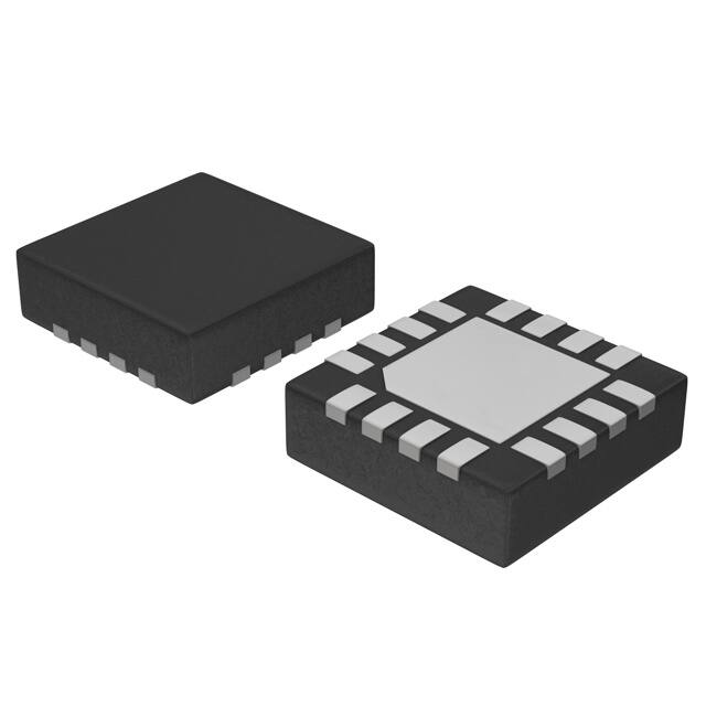
QFN−16
CASE 485AE
NLAB
4783
ALYWG
G
1
A = Assembly Location
L = Wafer Lot
Y = Year
W = Work Week
G = Pb−Free Package
(Note: Microdot may be in either location)
Typical Applications
•
•
•
•
ÇÇ
ÇÇ
16
• Single Supply Operation
Cell Phone Speaker/Microphone Switching
Ringtone−Chip/Amplifier Switching
Three Unbalanced (Single−Ended) Switches
Stereo Balanced (Push−Pull) Switching
PIN CONNECTIONS
Important Information
Y0
Y1
Vcc
Y
16
15
14
13
• ESD Protection:
•
•
•
•
Human Body Model (HBM) > 8000 V
Machine Model (MM) > 400 V
Ringtone−Chip/Amplifier Switching
Continuous Current Rating Through each Switch ±300 mA
Conforms to: JEDEC MO−220, Issue H, Variation VEED−6
Pin−for−Pin Compatible with MAX4783
Z1
1
12
X
Z
2
11
X1
Z0
3
10
X0
ENABLE
4
9
A
5
6
NC GND
7
8
C
B
ORDERING INFORMATION
See detailed ordering and shipping information in the package
dimensions section on page 10 of this data sheet.
*For additional information on our Pb−Free strategy and soldering details, please
download the ON Semiconductor Soldering and Mounting Techniques
Reference Manual, SOLDERRM/D.
© Semiconductor Components Industries, LLC, 2008
July, 2008 − Rev. 1
1
Publication Order Number:
NLAS4783B/D
�NLAS4783B
X, Y, or Z
X0, Y0, or Z0
ENABLE
LOGIC
X1, Y1, or Z1
A, B, or C
Figure 1. Input Equivalent Circuit
PIN FUNCTION DESCRIPTION
QFN PIN #
Symbol
Description
15
Y1
Analog Switch Y Normally Open Input
16
Y0
Analog Switch Y Normally Closed Input
1
Z1
Analog Switch Z Normally Open Input
2
Z
Analog Switch Z Output
3
Z0
Analog Switch Z Normally Closed Input
4
ENABLE
5
NC
6
GND
7
C
Digital Address C Input
8
B
Digital Address B Input
9
A
Digital Address A Input
10
X0
Analog Switch X Normally Closed Input
11
X1
Analog Switch X Normally Open Input
12
X
Analog Switch X Output
13
Y
Analog Switch Y Output
14
VCC
Digital Enable Input. Normally connect to GND. Drive to logic high to set all switches off.
No Connection. Not internally connected.
Ground
Positive Analog and Digital Supply Voltage Input
http://onsemi.com
2
�NLAS4783B
TRUTH TABLE/SWITCH PROGRAMMING
Select Input
Enable Input
C
B
A
H
X
X
X
All Switches Open
L
L
L
L
X−X0
Y−Y0
Z−Z0
L
L
L
H
X−X1
Y−Y0
Z−Z0
L
L
H
L
X−X0
Y−Y1
Z−Z0
L
L
H
H
X−X1
Y−Y1
Z−Z0
L
H
L
L
X−X0
Y−Y0
Z−Z1
L
H
L
H
X−X1
Y−Y0
Z−Z1
L
H
H
L
X−X0
Y−Y1
Z−Z1
L
H
H
H
X−X1
Y−Y1
Z−Z1
1. Input and output pins are identical and interchangeable. Both pins can be considered input or output. Bidirectional signal pass.
http://onsemi.com
3
�NLAS4783B
MAXIMUM RATINGS
Symbol
Parameter
Value
Unit
VCC
Positive DC Supply Voltage
*0.5 to )5.5
V
VIS
Analog Input Voltage (VNO, VNC, or VCOM)
*0.5 to VCC
V
VIN
Digital Select Input Voltage
*0.5 to )5.5
V
Ianl1
Continuous DC Current from COM to NC/NO
$300
mA
Peak Current from COM to NC/NO, 10 Duty Cycles (Note 2)
$500
mA
Continuous DC Current into COM/NC/NO with Respect to VCC or GND
$100
mA
Ianl−pk 1
Iclmp
Stresses exceeding Maximum Ratings may damage the device. Maximum Ratings are stress ratings only. Functional operation above the
Recommended Operating Conditions is not implied. Extended exposure to stresses above the Recommended Operating Conditions may affect
device reliability.
2. Defined as 10% ON, 90% off duty cycle.
RECOMMENDED OPERATING CONDITIONS
Symbol
Parameter
Min
Max
Unit
1.65
4.5
V
Analog Input Voltage (VNO, VNC, or VCOM)
−
VCC
V
VIN
Digital Select Input Voltage
−
VCC
V
TA
Operating Temperature Range
*40
85
°C
tr, tf
Input Rise or Fall Time, SELECT
−
−
20
10
ns/V
VCC
Positive DC Supply Voltage
VIS
VCC = 1.6−2.7 V
VCC = 3.0−4.5 V
http://onsemi.com
4
�NLAS4783B
DC CHARACTERISTICS − Digital Section (Voltages Referenced to GND)
Guaranteed Limit
Symbol
Parameter
Condition
VCC
*405C to 255C
t855C
Unit
VIH
Minimum High−Level Input
Voltage, Select Inputs
1.65
2.7
3.6
4.3
1.0
1.4
1.8
2.2
1.0
1.4
1.8
2.2
V
VIL
Maximum Low−Level Input
Voltage, Select Inputs
1.65
2.7
3.6
4.3
0.4
0.5
0.6
0.8
0.4
0.5
0.6
0.8
V
IIN
Maximum Input Leakage
Current, Select Inputs
VIN = 4.5 V or GND
4.3
$ 0.1
$ 1.0
�A
IOFF
Power Off Leakage Current
VIN = 4.5 V or GND
0
$0.5
$2.0
�A
ICC
Maximum Quiescent Supply
Current (Note 3)
Select and VIS = VCC or GND
1.65 to 4.5
$ 1.0
$ 2.0
�A
DC ELECTRICAL CHARACTERISTICS − Analog Section
Guaranteed Maximum Limit
−405C to 255C
Symbol
Max
t855C
Max
Unit
1.0
1.2
�
2.7 − 4.3
0.2
0.2
�
2.7 − 4.3
0.4
0.6
�
−100
100
nA
−100
100
nA
Condition
VCC
NC/NO On−Resistance
(Note 3)
VIN v VIL or VIN w VIH
VIS = GND to VCC
IINI v 100 mA
2.7 − 4.3
RFLAT
NC/NO On−Resistance Flatness
(Notes 3, 5)
ICOM = 100 mA
VIS = 0 to VCC
�RON
On−Resistance Match Between Channels
(Notes 3 and 4)
VIS = 0.5 VCC;
ICOM = 100 mA
INC(OFF)
INO(OFF)
NC or NO Off Leakage Current (Note 3)
VIN = VIL or VIH
VNO or VNC = 0.3 V
VCOM = 4.0 V
4.3
−10
10
ICOM(ON)
COM ON
Leakage Current
(Note 3)
VIN = VIL or VIH
VNO 0.3 V or 4.0 V with
VNC floating or
VNC 0.3 V or 4.0 V with
VNO floating
VCOM = 0.3 V or 4.0 V
4.3
−10
10
RON
Parameter
Min
Min
3. Guaranteed by design. Resistance measurements do not include test circuit or package resistance.
4. �RON = RON(MAX) − RON(MIN) between NC1 and NC2 or between NO1 and NO2.
5. Flatness is defined as the difference between the maximum and minimum value of on−resistance as measured over the specified analog
signal ranges.
http://onsemi.com
5
�NLAS4783B
AC ELECTRICAL CHARACTERISTICS (Input tr = tf = 3.0 ns)
Guaranteed Maximum Limit
Symbol
Parameter
Test Conditions
VCC
(V)
VIS
(V)
*405C to 255C
Min
Typ*
Max
t855C
Min
Max
Unit
tON
Turn−On Time
RL = 50 �� CL = 35 pF
(Figures 3 and 4)
2.3 − 4.5
1.5
25
27
ns
tOFF
Turn−Off Time
RL = 50 �� CL = 35 pF
(Figures 3 and 4)
2.3 − 4.5
1.5
15
20
ns
tBBM
Minimum Break−Before−Make Time
VIS = 3.0
RL = 300 �� CL = 35 pF
(Figure 2)
3.0
1.5
2.0
ns
8.0
Typical @ 25, VCC = 4.5 V
CIN
Control Pin Input Capacitance
5.0
pF
CSN
SN Port Capacitance
75
pF
CD
D Port Capacitance When Switch is Enabled
240
pF
*Typical Characteristics are at 25°C.
ADDITIONAL APPLICATION CHARACTERISTICS (Voltages Referenced to GND Unless Noted)
255C
VCC
(V)
Typical
Unit
Symbol
Parameter
BW
Maximum On−Channel −3dB
Bandwidth or Minimum Frequency
Response
VIN centered between VCC and GND
(Figure 5)
1.65 − 4.5
17
MHz
VONL
Maximum Feed−through On Loss
VIN = 0 dBm @ 100 kHz to 50 MHz
VIN centered between VCC and GND (Figure 5)
1.65 − 4.5
−0.10
dB
VISO
Off−Channel Isolation
f = 100 kHz; VIS = 1 V RMS; CL = 5 nF
VIN centered between VCC and GND(Figure 5) (Note 6)
1.65 − 4.5
−62
dB
Q
Charge Injection Select Input to
Common I/O
VIN = VCC to GND, RIS = 0 �, CL = 1 nF
Q = CL x �VOUT (Figure 6)
1.65 − 4.5
50
pC
THD
Total Harmonic Distortion THD +
Noise
FIS = 20 Hz to 20 kHz, RL = Rgen = 600 �, CL = 50 pF
VIS = 2 V RMS
4.5
0.008
%
VCT
Channel−to−Channel Crosstalk
f = 100 kHz; VIS = 1 V RMS, CL = 5 pF, RL = 50 �
VIN centered between VCC and GND (Figure 5)
1.65 − 4.5
−62
dB
Condition
6. Off−Channel Isolation = 20log10 (Vcom/Vno), Vcom = output, Vno = input to off switch.
http://onsemi.com
6
�NLAS4783B
VCC
DUT
VCC
Input
Output
GND
VOUT
0.1 �F
50 �
tBMM
35 pF
90%
90% of VOH
Output
Switch Select Pin
GND
Figure 2. tBBM (Time Break−Before−Make)
VCC
Input
DUT
VCC
0.1 �F
50%
Output
VOUT
Open
50%
0V
50 �
VOH
90%
35 pF
90%
Output
VOL
Input
tON
tOFF
Figure 3. tON/tOFF
VCC
VCC
Input
DUT
Output
50%
50 �
VOUT
Open
50%
0V
VOH
35 pF
Output
10%
VOL
Input
tOFF
Figure 4. tON/tOFF
http://onsemi.com
7
10%
tON
�NLAS4783B
50 �
DUT
Reference
Transmitted
Input
Output
50 � Generator
50 �
Channel switch control/s test socket is normalized. Off isolation is measured across an off channel. On loss is
the bandwidth of an On switch. VISO, Bandwidth and VONL are independent of the input signal direction.
ǒVVOUT
Ǔ for VIN at 100 kHz
IN
VOUT
Ǔ for VIN at 100 kHz to 50 MHz
VONL = On Channel Loss = 20 Log ǒ
VIN
VISO = Off Channel Isolation = 20 Log
Bandwidth (BW) = the frequency 3 dB below VONL
VCT = Use VISO setup and test to all other switch analog input/outputs terminated with 50 �
Figure 5. Off Channel Isolation/On Channel Loss (BW)/Crosstalk
(On Channel to Off Channel)/VONL
DUT
VCC
VIN
Output
Open
GND
CL
Output
Off
VIN
Figure 6. Charge Injection: (Q)
http://onsemi.com
8
On
Off
�VOUT
�NLAS4783B
1.2
1.2
85°C
1.0
25°C
0.8
0.8
−40°C
RON (�)
RON (�)
1.0
0.6
0.4
0.2
0.2
0.5
0
1.0
1.5
2.0
2.5
3.0
3.5
4.0
0
0.0
4.5
0.5
1.0
1.5
2.0
2.5
3.0
VIN (V)
Figure 7. On−Resistance vs. Input Voltage
@ VCC = 4.3 V
Figure 8. RON vs. VIN vs. Temperature
@ VCC = 3.0 V
0.008
85°C
1.0
0.007
25°C
0.006
−40°C
THD (%)
RON (�)
−40°C
VIN (V)
1.2
0.8
25°C
0.6
0.4
0
85°C
0.6
0.4
0.005
0.004
0.003
0.002
0.2
0.0
0.0
0.001
0.5
1.0
1.5
2.0
2.5
3.0
3.5
0
4.0
10
VIN (V)
100
1000
10000
100000
FREQUENCY (Hz)
Figure 9. RON vs. VIN vs. Temperature
@ VCC = 3.6 V
Figure 10. Total Harmonic Distortion vs.
Frequency
http://onsemi.com
9
�NLAS4783B
ORDERING INFORMATION
Device Nomenclature
Device Order
Number
Circuit
Indicator
Technology
Device
Function
Package
Suffix
Tape & Reel
Suffix
NLAS4783BMN1R2G
NL
AS
4783B
MN1
R2G
Package Type
Tape & Reel Size†
QFN
(Pb−Free)
3000 Tape & Reel
†For information on tape and reel specifications, including part orientation and tape sizes, please refer to our Tape and Reel Packaging
Specifications Brochure, BRD8011/D.
http://onsemi.com
10
�MECHANICAL CASE OUTLINE
PACKAGE DIMENSIONS
QFN16 3x3, 0.5P
CASE 485AE
ISSUE C
1
SCALE 2:1
ÇÇ
ÇÇ
ÇÇ
PIN 1
LOCATION
D
A
B
L1
DETAIL A
ALTERNATE TERMINAL
CONSTRUCTIONS
E
ÉÉÉ
ÉÉÉ
EXPOSED Cu
TOP VIEW
0.10 C
16X
L
A1
SIDE VIEW
DETAIL A
5
SEATING
PLANE
XXXXX
XXXXX
ALYWG
G
9
E2
1
b
0.10 C A B
16X
A
L
Y
W
G
12
16
e
e/2
NOTE 3
RECOMMENDED
SOLDERING FOOTPRINT*
13
BOTTOM VIEW
MILLIMETERS
MIN
MAX
0.80
1.00
0.00
0.05
0.20 REF
0.18
0.30
3.00 BSC
1.25
1.55
3.00 BSC
1.25
1.55
0.50 BSC
0.20
−−−
0.30
0.50
0.00
0.15
GENERIC
MARKING DIAGRAM*
8
K
0.05 C
C
D2
4
16X
MOLD CMPD
ALTERNATE
CONSTRUCTIONS
A
0.08 C
ÉÉ
ÉÉ
ÇÇ
DIM
A
A1
A3
b
D
D2
E
E2
e
K
L
L1
A3
A1
DETAIL B
(A3)
DETAIL B
NOTE 4
NOTES:
1. DIMENSIONING AND TOLERANCING PER
ASME Y14.5M, 1994.
2. CONTROLLING DIMENSION: MILLIMETERS.
3. DIMENSION b APPLIES TO PLATED
TERMINAL AND IS MEASURED BETWEEN
0.25 AND 0.30 MM FROM TERMINAL.
4. COPLANARITY APPLIES TO THE EXPOSED
PAD AS WELL AS THE TERMINALS.
5. OUTLINE MEETS JEDEC DIMENSIONS PER
MO−220, VARIATION VEED−6.
L
L
0.15 C
0.15 C
DATE 24 JUN 2016
3.30
PACKAGE
OUTLINE
16X
0.65
1.55
1
= Assembly Location
= Wafer Lot
= Year
= Work Week
= Pb−Free Package
(Note: Microdot may be in either location)
*This information is generic. Please refer to
device data sheet for actual part marking.
Pb−Free indicator, “G” or microdot “ G”,
may or may not be present.
1.55 3.30
16X
0.30
0.50
PITCH
DIMENSIONS: MILLIMETERS
*For additional information on our Pb−Free strategy and soldering
details, please download the ON Semiconductor Soldering and
Mounting Techniques Reference Manual, SOLDERRM/D.
DOCUMENT NUMBER:
DESCRIPTION:
98AON14949D
QFN16 3X3, 0.5P
Electronic versions are uncontrolled except when accessed directly from the Document Repository.
Printed versions are uncontrolled except when stamped “CONTROLLED COPY” in red.
PAGE 1 OF 1
ON Semiconductor and
are trademarks of Semiconductor Components Industries, LLC dba ON Semiconductor or its subsidiaries in the United States and/or other countries.
ON Semiconductor reserves the right to make changes without further notice to any products herein. ON Semiconductor makes no warranty, representation or guarantee regarding
the suitability of its products for any particular purpose, nor does ON Semiconductor assume any liability arising out of the application or use of any product or circuit, and specifically
disclaims any and all liability, including without limitation special, consequential or incidental damages. ON Semiconductor does not convey any license under its patent rights nor the
rights of others.
© Semiconductor Components Industries, LLC, 2019
www.onsemi.com
�onsemi,
, and other names, marks, and brands are registered and/or common law trademarks of Semiconductor Components Industries, LLC dba “onsemi” or its affiliates
and/or subsidiaries in the United States and/or other countries. onsemi owns the rights to a number of patents, trademarks, copyrights, trade secrets, and other intellectual property.
A listing of onsemi’s product/patent coverage may be accessed at www.onsemi.com/site/pdf/Patent−Marking.pdf. onsemi reserves the right to make changes at any time to any
products or information herein, without notice. The information herein is provided “as−is” and onsemi makes no warranty, representation or guarantee regarding the accuracy of the
information, product features, availability, functionality, or suitability of its products for any particular purpose, nor does onsemi assume any liability arising out of the application or use
of any product or circuit, and specifically disclaims any and all liability, including without limitation special, consequential or incidental damages. Buyer is responsible for its products
and applications using onsemi products, including compliance with all laws, regulations and safety requirements or standards, regardless of any support or applications information
provided by onsemi. “Typical” parameters which may be provided in onsemi data sheets and/or specifications can and do vary in different applications and actual performance may
vary over time. All operating parameters, including “Typicals” must be validated for each customer application by customer’s technical experts. onsemi does not convey any license
under any of its intellectual property rights nor the rights of others. onsemi products are not designed, intended, or authorized for use as a critical component in life support systems
or any FDA Class 3 medical devices or medical devices with a same or similar classification in a foreign jurisdiction or any devices intended for implantation in the human body. Should
Buyer purchase or use onsemi products for any such unintended or unauthorized application, Buyer shall indemnify and hold onsemi and its officers, employees, subsidiaries, affiliates,
and distributors harmless against all claims, costs, damages, and expenses, and reasonable attorney fees arising out of, directly or indirectly, any claim of personal injury or death
associated with such unintended or unauthorized use, even if such claim alleges that onsemi was negligent regarding the design or manufacture of the part. onsemi is an Equal
Opportunity/Affirmative Action Employer. This literature is subject to all applicable copyright laws and is not for resale in any manner.
PUBLICATION ORDERING INFORMATION
LITERATURE FULFILLMENT:
Email Requests to: orderlit@onsemi.com
onsemi Website: www.onsemi.com
◊
TECHNICAL SUPPORT
North American Technical Support:
Voice Mail: 1 800−282−9855 Toll Free USA/Canada
Phone: 011 421 33 790 2910
Europe, Middle East and Africa Technical Support:
Phone: 00421 33 790 2910
For additional information, please contact your local Sales Representative
�


 工商网监
湘ICP备2023018690号
工商网监
湘ICP备2023018690号
