NLSF1174
Hex D Flip−Flop with
Common Clock and Reset
This device consists of six D flip−flops with common Clock and
Reset inputs. Each flip−flop is loaded with a low−to−high transition of
the Clock input. Reset is asynchronous and active low. All
inputs/outputs are standard CMOS compatible.
http://onsemi.com
Features
•
•
•
•
•
•
•
Output Drive Compatibility: 10 LSTTL Loads
Outputs Directly Interface to CMOS
Operating Voltage Range: 2.0 to 6.0 V
Low Input Current: 1.0 mA
MSL Level 1
Chip Complexity: 162 FET
Pb−Free Package is Available*
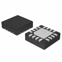
QFN−16
MN SUFFIX
CASE 485G
1
MARKING DIAGRAM
ÇÇÇ
ÇÇÇ
16
1
Q0
Reset
VCC
Q5
16
15
14
13
NLSF
1174
ALYW G
G
D0
1
12
D5
D1
2
11
D4
Q1
3
10
Q4
D2
4
9
D3
NLSF1174
A
L
Y
W
G
= Device Code
= Assembly Location
= Wafer Lot
= Year
= Work Week
= Pb−Free Package
(Note: Microdot may be in either location)
FUNCTION TABLE
Inputs
5
Q2
6
GND
7
Clock
8
Q3
Center pad on bottom may be connected to VCC of device.
This pad must be isolated or connected to VCC.
Reset
Clock
L
X
Output
D
Q
X
L
H
H
H
H
L
L
X
No Change
X
No Change
H
L
H
Figure 1. PIN ASSIGNMENT (Top View)
ORDERING INFORMATION
Device
NLSF1174MNR2
NLSF1174MNR2G
*For additional information on our Pb−Free strategy and soldering details, please
download the ON Semiconductor Soldering and Mounting Techniques
Reference Manual, SOLDERRM/D.
© Semiconductor Components Industries, LLC, 2006
May, 2006 − Rev. 5
1
Package
Shipping†
QFN−16
3000 / Tape & Reel
QFN−16 3000 / Tape & Reel
(Pb−Free)
†For information on tape and reel specifications,
including part orientation and tape sizes, please
refer to our Tape and Reel Packaging Specifications
Brochure, BRD8011/D.
Publication Order Number:
NLSF1174/D
�NLSF1174
DATA
INPUTS
D0
Q0
D1
Q1
D2
D3
Q2
D4
Q4
D5
Q5
NONINVERTING
OUTPUTS
Q3
CLOCK
RESET
Figure 2. LOGIC DIAGRAM
DESIGN/VALUE TABLE
Design Criteria
Value
Unit
Internal Gate Count*
40.5
ea
Internal Gate Propagation Delay
1.5
ns
Internal Gate Power Dissipation
5.0
mW
.0075
pJ
Symbol
Value
Unit
Speed Power Product
*Equivalent to a two−input NAND gate.
MAXIMUM RATINGS
Parameter
DC Supply Voltage
(Referenced to GND)
VCC
*0.5 to )7.0
V
DC Input Voltage
(Referenced to GND)
VIN
*1.5 to VCC )1.5
V
VOUT
*0.5 to VCC )0.5
V
IIN
$20
mA
DC Output Current, per Pin
IOUT
$25
mA
DC Supply Current, VCC and GND Pins
ICC
$50
mA
TSTG
*65 to )150
°C
PDIP, SOIC, TSSOP
TL
260
°C
TJ
)150
°C
Thermal Resistance
QFN
qJA
80
°C/W
Power Dissipation in Still Air at 85°C
QFN
PD
800
mW
MSL
Level 1
FR
UL 94 V−0 @ 0.125 in
VESD
u2000
u100
u500
V
ILATCHUP
$300
mA
DC Output Voltage
(Referenced to GND) (Note 1)
DC Input Current, per Pin
Storage Temperature Range
Lead Temperature, 1 mm from Case for 10 Seconds
Junction Temperature Under Bias
Moisture Sensitivity
Flammability Rating
ESD Withstand Voltage
Latchup Performance
Oxygen Index: 30 to 35
Human Body Model (Note 2)
Machine Model (Note 3)
Charged Device Model (Note 4)
Above VCC and Below GND at 85°C (Note 5)
Stresses exceeding Maximum Ratings may damage the device. Maximum Ratings are stress ratings only. Functional operation above the
Recommended Operating Conditions is not implied. Extended exposure to stresses above the Recommended Operating Conditions may affect
device reliability.
1. IO absolute maximum rating must be observed.
2. Tested to EIA/JESD22−A114−A.
3. Tested to EIA/JESD22−A115−A.
4. Tested to JESD22−C101−A.
5. Tested to EIA/JESD78.
6. For high frequency or heavy load considerations, see the ON Semiconductor High−Speed CMOS Data Book (DL129/D).
http://onsemi.com
2
�NLSF1174
RECOMMENDED OPERATING CONDITIONS
ÎÎÎÎÎÎÎÎÎÎÎÎÎÎÎÎÎÎÎÎÎÎÎÎÎÎÎÎÎÎÎÎÎÎÎÎÎ
ÎÎÎÎÎÎÎÎÎÎÎÎÎÎÎÎÎÎÎÎÎÎÎÎÎÎÎÎÎÎÎÎÎÎÎÎÎ
ÎÎÎÎÎÎÎÎÎÎÎÎÎÎÎÎÎÎÎÎÎÎÎÎÎÎÎÎÎÎÎÎÎÎÎÎÎ
ÎÎÎÎÎÎÎÎÎÎÎÎÎÎÎÎÎÎÎÎÎÎÎ
ÎÎÎÎÎ
ÎÎÎ
ÎÎÎÎ
ÎÎ
ÎÎÎÎÎÎÎÎÎÎÎÎÎÎÎÎÎÎÎÎÎÎÎ
ÎÎÎÎÎ
ÎÎÎ
ÎÎÎÎ
ÎÎ
ÎÎÎÎÎÎÎÎÎÎÎÎÎÎÎÎÎÎÎÎÎÎÎÎÎÎÎÎÎÎÎÎÎÎÎÎÎ
Parameter
DC Supply Voltage
(Referenced to GND)
DC Input Voltage, Output Voltage
(Referenced to GND) (Note 7)
Symbol
Min
Max
Unit
VCC
2.0
6.0
V
VIN, VOUT
0
VCC
V
TA
*55
)125
°C
tr, tf
0
0
0
1000
500
400
ns
Operating Temperature, All Package Types
Input Rise and Fall Time (Figure 4)
VCC = 2.0 V
VCC = 4.5 V
VCC = 6.0 V
7. Unused inputs may not be left open. All inputs must be tied to a high− or low−logic input voltage level.
DC ELECTRICAL CHARACTERISTICS (Voltages Referenced to GND)
ÎÎÎÎÎÎÎÎÎÎÎ
ÎÎÎÎÎÎÎÎ
ÎÎÎÎÎÎÎÎÎÎÎ
ÎÎÎÎÎÎÎÎ
ÎÎÎÎÎÎÎÎÎÎÎÎÎÎÎÎÎÎÎ
ÎÎÎÎÎÎÎÎÎÎÎÎÎÎÎÎÎÎÎ
ÎÎÎÎÎÎÎÎ
ÎÎÎÎÎÎÎÎÎÎÎ
ÎÎÎÎÎÎÎÎÎÎÎ
ÎÎÎÎÎÎÎÎ
ÎÎÎÎÎÎÎÎÎÎÎ
ÎÎÎÎÎÎÎÎ
ÎÎÎÎÎÎÎÎÎÎÎ
ÎÎÎÎÎÎÎÎ
ÎÎÎÎÎÎÎÎÎÎÎÎÎÎÎÎÎÎÎ
ÎÎÎÎÎÎÎÎÎÎÎ
ÎÎÎÎÎÎÎÎ
ÎÎÎÎÎÎÎÎÎÎÎ
ÎÎÎÎÎÎÎÎ
ÎÎÎÎÎÎÎÎÎÎÎ
ÎÎÎÎÎÎÎÎ
ÎÎÎÎÎÎÎÎÎÎÎÎÎÎÎÎÎÎÎ
ÎÎÎÎÎÎÎÎÎÎÎÎÎÎÎÎÎÎÎ
ÎÎÎÎÎÎÎÎÎÎÎ
ÎÎÎÎÎÎÎÎ
ÎÎÎÎÎÎÎÎÎÎÎÎÎÎÎÎÎÎÎ
Test Conditions
Symbol
Minimum High−Level Input Voltage
VOUT = 0.1 V or VCC – 0.1 V
|IOUT| v 20 mA
VIH
Maximum Low−Level Input Voltage
VOUT = 0.1 V or VCC – 0.1 V
|IOUT| v 20 mA
VIL
Minimum High−Level Output Voltage
VIN = VIH or VIL
|IOUT| v 20 mA
VOH
Parameter
VIN = VIH or VIL
|IOUT| v 4.0 mA
|IOUT| v 5.2 mA
Maximum Low−Level Output Voltage
VIN = VIH or VIL
|IOUT| v 20 mA
Guaranteed Limit
VCC
VOL
VIN = VIH or VIL
|IOUT| v 4.0 mA
|IOUT| v 5.2 mA
Maximum Input Leakage Current
VIN = VCC or GND
IIN
Maximum Quiescent Supply Current
(per Package)
VIN = VCC or GND
IOUT = 0 mA
ICC
ÎÎÎ
ÎÎÎÎÎ
ÎÎÎ
ÎÎÎÎ
ÎÎ
ÎÎÎÎÎÎÎÎÎÎÎÎÎÎÎÎÎ
ÎÎÎ
ÎÎÎÎÎÎÎÎÎÎÎÎÎÎ
ÎÎÎÎÎÎÎÎÎÎÎÎÎÎÎÎÎ
ÎÎÎ
ÎÎÎÎÎÎÎÎÎÎÎÎÎÎ
ÎÎÎÎÎÎÎÎÎÎÎÎÎÎÎÎÎ
ÎÎÎ
ÎÎÎÎÎÎÎÎÎÎÎÎÎÎ
ÎÎÎÎÎÎÎÎÎÎÎÎÎÎÎÎÎ
ÎÎÎ
ÎÎÎÎÎÎÎÎÎÎÎÎÎÎ
ÎÎÎÎÎÎÎÎÎÎÎÎÎÎÎÎÎ
ÎÎÎ
ÎÎÎÎÎÎÎÎÎÎÎÎÎÎ
ÎÎ
ÎÎÎ
ÎÎÎÎÎ
ÎÎÎ
ÎÎÎÎ
ÎÎÎ
ÎÎÎÎÎÎÎÎÎÎÎÎÎÎ
ÎÎÎ
ÎÎÎÎÎ
ÎÎÎ
ÎÎÎÎ
ÎÎ
ÎÎÎ
ÎÎÎÎÎ
ÎÎÎ
ÎÎÎÎ
ÎÎ
ÎÎÎ
ÎÎÎÎÎÎÎÎÎÎÎÎÎÎ
V
*555C to 255C
v855C
v1255C
Unit
2.0
4.5
6.0
1.5
3.15
4.2
1.5
3.15
4.2
1.5
3.15
4.2
V
2.0
4.5
6.0
0.5
1.35
1.8
0.5
1.35
1.8
0.5
1.35
1.8
V
2.0
4.5
6.0
1.9
4.4
5.9
1.9
4.4
5.9
1.9
4.4
5.9
V
4.5
6.0
3.98
5.48
3.84
5.34
3.7
5.2
2.0
4.5
6.0
0.1
0.1
0.1
0.1
0.1
0.1
0.1
0.1
0.1
4.5
6.0
0.26
0.26
0.33
0.33
0.4
0.4
6.0
$0.1
$1.0
$1.0
mA
6.0
4.0
40
160
mA
V
8. Information on typical parametric values, along with high frequency or heavy load considerations, can be found in the ON Semiconductor
High−Speed CMOS Data Book (DL129/D).
AC ELECTRICAL CHARACTERISTICS (CL = 50 pF, Input tr = tf = 6.0 ns)
ÎÎÎÎÎÎÎÎÎÎÎÎÎÎÎÎÎÎ
ÎÎÎÎÎÎÎÎÎÎÎÎÎÎÎÎÎÎ
ÎÎÎÎÎÎÎÎÎÎÎÎÎÎÎÎÎÎ
ÎÎÎÎÎÎÎÎÎÎÎÎÎÎÎÎÎÎ
ÎÎÎÎÎÎÎÎÎÎÎÎÎÎÎÎÎÎ
ÎÎÎÎÎÎÎÎÎÎÎÎÎÎÎÎÎÎ
ÎÎÎÎÎÎÎÎÎÎÎÎÎÎÎÎÎÎ
ÎÎÎÎÎÎÎÎÎÎÎÎÎÎÎÎÎÎ
ÎÎÎÎÎÎÎÎÎÎÎÎÎÎÎÎÎÎ
ÎÎÎÎÎÎÎÎÎÎÎÎÎÎÎÎÎÎ
ÎÎÎÎÎÎÎÎÎÎÎÎÎÎÎÎÎÎ
ÎÎÎÎÎÎÎÎÎÎÎÎÎÎÎÎÎÎ
ÎÎÎ
ÎÎÎÎÎ
ÎÎÎ
ÎÎÎÎÎ
ÎÎ
ÎÎÎ
ÎÎÎÎÎÎÎÎ
ÎÎÎÎÎÎÎ
ÎÎÎ
ÎÎÎÎÎÎÎÎ
ÎÎÎ
ÎÎÎÎÎÎÎ
ÎÎÎ
ÎÎÎÎÎ
ÎÎÎÎÎ
ÎÎ
ÎÎÎ
ÎÎÎÎÎ
ÎÎÎ
ÎÎÎÎÎ
ÎÎ
ÎÎÎ
ÎÎÎÎÎ
ÎÎÎ
ÎÎÎÎÎ
ÎÎ
ÎÎÎ
ÎÎÎÎÎÎÎÎ
ÎÎÎÎÎÎÎ
ÎÎÎ
ÎÎÎÎÎ
ÎÎÎ
ÎÎÎÎÎ
ÎÎ
ÎÎÎ
ÎÎÎÎÎÎÎÎ
ÎÎÎÎÎÎÎ
ÎÎÎÎÎÎÎÎÎÎÎÎÎÎÎÎÎÎ
Symbol
Parameter
Maximum Clock Frequency (50% Duty Cycle)
(Figures 4 and 7)
fmax
Maximum Propagation Delay, Clock to Q
(Figures 5 and 7)
tPLH
tPHL
Maximum Propagation Delay, Reset to Q
(Figures 2 and 7)
tPLH
tPHL
Maximum Output Transition Time, Any Output
(Figures 4 and 7)
tTLH
tTHL
Maximum Input Capacitance
Cin
Guaranteed Limit
VCC
V
*555C to 255C
v855C
v1255C
Unit
2.0
4.5
6.0
6.0
30
35
4.8
24
28
4.0
20
24
MHz
2.0
4.5
6.0
110
22
19
140
28
24
165
33
28
ns
2.0
4.5
6.0
110
21
19
140
28
24
160
32
27
ns
2.0
4.5
6.0
75
15
13
95
19
16
110
22
19
ns
10
10
10
pF
Typical @ 255C, VCC = 5.0 V
62
pF
Power Dissipation Capacitance, per Enabled Output (Note 10)
CPD
9. For propagation delays with loads other than 50 pF, and information on typical parametric values, see the ON Semiconductor High−Speed
CMOS Data Book (DL129/D).
10. Used to determine the no−load dynamic power consumption: P D = C PD V CC 2 f + I CC V CC . For load considerations, see the ON
Semiconductor High−Speed CMOS Data Book (DL129/D).
http://onsemi.com
3
�NLSF1174
TIMING REQUIREMENTS (CL = 50 pF, Input tr = tf = 6.0 ns)
Guaranteed Limit
ÎÎÎÎÎÎÎÎÎÎÎÎÎÎ
ÎÎÎ
ÎÎÎÎÎÎÎÎÎÎÎÎÎÎ
ÎÎÎ
ÎÎÎÎÎÎÎÎÎÎÎÎÎÎÎÎÎ
ÎÎÎÎÎÎÎÎÎÎÎÎÎÎ
ÎÎÎ
ÎÎÎÎÎÎÎÎÎÎÎÎÎÎÎÎÎ
ÎÎÎÎÎÎÎÎÎÎÎÎÎÎ
ÎÎÎ
ÎÎÎÎÎÎÎÎÎÎÎÎÎÎÎÎÎ
ÎÎÎÎÎÎÎÎÎÎÎÎÎÎ
ÎÎÎ
ÎÎÎÎÎÎÎÎÎÎÎÎÎÎÎÎÎ
ÎÎÎÎÎÎÎÎÎÎÎÎÎÎ
ÎÎÎ
ÎÎÎÎÎÎÎÎÎÎÎÎÎÎÎÎÎ
ÎÎÎÎÎÎÎÎÎÎÎÎÎÎ
ÎÎÎ
ÎÎÎÎÎÎÎÎÎÎÎÎÎÎÎÎÎ
Parameter
*555C to 255C
VCC
V
v855C
v1255C
ÎÎÎ
ÎÎÎ
ÎÎÎ
ÎÎÎ
ÎÎÎ
ÎÎÎ
ÎÎÎ
ÎÎ
ÎÎÎ
ÎÎÎ
ÎÎÎ
ÎÎÎ
ÎÎÎ
ÎÎÎ
ÎÎÎ
ÎÎ
ÎÎÎÎÎÎÎÎÎÎÎÎÎÎÎÎÎÎÎÎÎÎÎ
ÎÎÎ
ÎÎÎ
ÎÎÎ
ÎÎÎ
ÎÎÎ
ÎÎÎ
ÎÎÎ
ÎÎ
ÎÎÎÎÎÎÎÎÎÎÎÎÎÎÎÎÎÎÎÎÎÎÎ
ÎÎÎ
ÎÎÎ
ÎÎÎ
ÎÎÎ
ÎÎÎ
ÎÎÎ
ÎÎÎ
ÎÎ
ÎÎÎÎÎÎÎÎÎÎÎÎÎÎÎÎÎÎÎÎÎÎÎ
ÎÎÎ
ÎÎÎ
ÎÎÎ
ÎÎÎ
ÎÎÎ
ÎÎÎ
ÎÎÎ
ÎÎ
ÎÎÎÎÎÎÎÎÎÎÎÎÎÎÎÎÎÎÎÎÎÎÎ
ÎÎÎ
ÎÎÎ
ÎÎÎ
ÎÎÎ
ÎÎÎ
ÎÎÎ
ÎÎÎ
ÎÎ
ÎÎÎÎÎÎÎÎÎÎÎÎÎÎÎÎÎÎÎÎÎÎÎ
ÎÎÎ
ÎÎÎ
ÎÎÎ
ÎÎÎ
ÎÎÎ
ÎÎÎ
ÎÎÎ
ÎÎ
ÎÎÎÎÎÎÎÎÎÎÎÎÎÎÎÎÎÎÎÎÎÎÎ
Figure
Symbol
Minimum Setup Time, Data to Clock
6
tsu
Minimum Hold Time, Clock to Data
6
th
Minimum Recovery Time,
Reset Inactive to Clock
5
trec
Minimum Pulse Width, Clock
4
tw
Minimum Pulse Width, Reset
5
tw
Maximum Input Rise and Fall Times
4
tr, tf
CLOCK
Min
Min
Max
Unit
75
15
13
ns
2.0
4.5
6.0
5.0
5.0
5.0
5.0
5.0
5.0
5.0
5.0
5.0
ns
2.0
4.5
6.0
5.0
5.0
5.0
5.0
5.0
5.0
5.0
5.0
5.0
ns
2.0
4.5
6.0
75
15
13
95
19
16
110
22
19
ns
2.0
4.5
6.0
75
15
13
95
19
16
110
22
19
ns
2.0
4.5
6.0
1000
500
400
Q
Q0
Q
Q1
Q
Q2
Q
Q3
Q
Q4
Q
Q5
R
RESET
C
D1
D
D2
D
R
C
R
C
D3
D
D4
D
R
C
R
C
D
R
Figure 3. Expanded Logic Diagram
http://onsemi.com
4
Max
65
13
11
D
D5
Min
50
10
9.0
C
D0
Max
2.0
4.5
6.0
1000
500
400
1000
500
400
ns
�NLSF1174
tr
CLOCK
tf
VCC
90%
50%
10%
tw
tw
RESET
VCC
50%
GND
GND
tPHL
1/fmax
tPLH
Q
Q
tPHL
trec
90%
50%
10%
CLOCK
tTLH
GND
tTHL
Figure 4. Switching Waveform
Figure 5. Switching Waveform
TEST POINT
VALID
VCC
DATA
VCC
50%
OUTPUT
50%
DEVICE
UNDER
TEST
GND
tsu
th
CL *
VCC
CLOCK
50%
GND
*Includes all probe and jig capacitance
Figure 6. Switching Waveform
Figure 7. Test Circuit
PIN1/PRODUCT ORIENTATION CARRIER TAPE
USER DIRECTION OF FEED
Figure 8.
http://onsemi.com
5
�MECHANICAL CASE OUTLINE
PACKAGE DIMENSIONS
QFN16 3x3, 0.5P
CASE 485G
ISSUE G
1
SCALE 2:1
DATE 08 OCT 2021
GENERIC
MARKING DIAGRAM*
XXXXX
XXXXX
ALYWG
G
XXXXX
A
L
Y
W
G
= Specific Device Code
= Assembly Location
= Wafer Lot
= Year
= Work Week
= Pb−Free Package
(Note: Microdot may be in either location)
*This information is generic. Please refer to
device data sheet for actual part marking.
Pb−Free indicator, “G” or microdot “G”, may
or may not be present. Some products may
not follow the Generic Marking.
DOCUMENT NUMBER:
DESCRIPTION:
98AON04795D
QFN16 3X3, 0.5P
Electronic versions are uncontrolled except when accessed directly from the Document Repository.
Printed versions are uncontrolled except when stamped “CONTROLLED COPY” in red.
PAGE 1 OF 1
onsemi and
are trademarks of Semiconductor Components Industries, LLC dba onsemi or its subsidiaries in the United States and/or other countries. onsemi reserves
the right to make changes without further notice to any products herein. onsemi makes no warranty, representation or guarantee regarding the suitability of its products for any particular
purpose, nor does onsemi assume any liability arising out of the application or use of any product or circuit, and specifically disclaims any and all liability, including without limitation
special, consequential or incidental damages. onsemi does not convey any license under its patent rights nor the rights of others.
© Semiconductor Components Industries, LLC, 2019
www.onsemi.com
�onsemi,
, and other names, marks, and brands are registered and/or common law trademarks of Semiconductor Components Industries, LLC dba “onsemi” or its affiliates
and/or subsidiaries in the United States and/or other countries. onsemi owns the rights to a number of patents, trademarks, copyrights, trade secrets, and other intellectual property.
A listing of onsemi’s product/patent coverage may be accessed at www.onsemi.com/site/pdf/Patent−Marking.pdf. onsemi reserves the right to make changes at any time to any
products or information herein, without notice. The information herein is provided “as−is” and onsemi makes no warranty, representation or guarantee regarding the accuracy of the
information, product features, availability, functionality, or suitability of its products for any particular purpose, nor does onsemi assume any liability arising out of the application or use
of any product or circuit, and specifically disclaims any and all liability, including without limitation special, consequential or incidental damages. Buyer is responsible for its products
and applications using onsemi products, including compliance with all laws, regulations and safety requirements or standards, regardless of any support or applications information
provided by onsemi. “Typical” parameters which may be provided in onsemi data sheets and/or specifications can and do vary in different applications and actual performance may
vary over time. All operating parameters, including “Typicals” must be validated for each customer application by customer’s technical experts. onsemi does not convey any license
under any of its intellectual property rights nor the rights of others. onsemi products are not designed, intended, or authorized for use as a critical component in life support systems
or any FDA Class 3 medical devices or medical devices with a same or similar classification in a foreign jurisdiction or any devices intended for implantation in the human body. Should
Buyer purchase or use onsemi products for any such unintended or unauthorized application, Buyer shall indemnify and hold onsemi and its officers, employees, subsidiaries, affiliates,
and distributors harmless against all claims, costs, damages, and expenses, and reasonable attorney fees arising out of, directly or indirectly, any claim of personal injury or death
associated with such unintended or unauthorized use, even if such claim alleges that onsemi was negligent regarding the design or manufacture of the part. onsemi is an Equal
Opportunity/Affirmative Action Employer. This literature is subject to all applicable copyright laws and is not for resale in any manner.
PUBLICATION ORDERING INFORMATION
LITERATURE FULFILLMENT:
Email Requests to: orderlit@onsemi.com
onsemi Website: www.onsemi.com
◊
TECHNICAL SUPPORT
North American Technical Support:
Voice Mail: 1 800−282−9855 Toll Free USA/Canada
Phone: 011 421 33 790 2910
Europe, Middle East and Africa Technical Support:
Phone: 00421 33 790 2910
For additional information, please contact your local Sales Representative
�