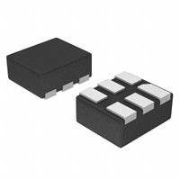
NLSV1T244MUTBG

NLSV1T244MUTBG

  • 厂商:

    ONSEMI(安森美)

  • 封装:

    UDFN6_1.4X1.2MM

  • 描述:

    NLSV1T244 是一款 1 位可配置双电源电压电平转换器。输入 An 和输出 Bn 端口设计用于分别跟踪两个不同的电源轨 VCCA 和 VCCB。两个电源轨都可在 0.9 V 至 4.5 V 范围...

  • 详情介绍
  • 数据手册
  • 价格&库存
NLSV1T244MUTBG 数据手册
NLSV1T244 1-Bit Dual-Supply Non-Inverting Level Translator The NLSV1T244 is a 1−bit configurable dual−supply voltage level translator. The input An and output Bn ports are designed to track two different power supply rails, VCCA and VCCB respectively. Both supply rails are configurable from 0.9 V to 4.5 V allowing universal low−voltage translation from the input An to the output Bn port. Features • • • • • • • • • • www.onsemi.com MARKING DIAGRAM 1 Wide VCCA and VCCB Operating Range: 0.9 V to 4.5 V High−Speed w/ Balanced Propagation Delay Inputs and Outputs have OVT Protection to 4.5 V Non−preferential VCCA and VCCB Sequencing Outputs at 3−State until Active VCC is Reached Power−Off Protection Outputs Switch to 3−State with VCCB at GND Ultra−Small Packaging: 1.2 mm x 1.0 mm UDFN6 NLVSV Prefix for Automotive and Other Applications Requiring Unique Site and Control Change Requirements; AEC−Q100 Qualified and PPAP Capable These Devices are Pb−Free, Halogen Free/BFR Free and are RoHS Compliant Q M = Specific Device Code = Date Code PIN ASSIGNMENT VCCA 1 6 VCCB A 2 5 B GND 3 4 OE (Top View) Typical Applications • Mobile Phones, PDAs, Other Portable Devices ORDERING INFORMATION Important Information Device • ESD Protection for All Pins: Shipping† 3000 / Tape & Reel †For information on tape and reel specifications, including part orientation and tape sizes, please refer to our Tape and Reel Packaging Specification Brochure, BRD8011/D. VCCB B A Package NLSV1T244MUTBG, UDFN6 NLVSV1T244MUTBG (Pb−Free) HBM (Human Body Model) > 3000 V VCCA QM UDFN6 MU SUFFIX CASE 517AA OE Figure 1. Logic Diagram © Semiconductor Components Industries, LLC, 2012 September, 2017 − Rev. 3 1 Publication Order Number: NLSV1T244/D NLSV1T244 PIN ASSIGNMENT TRUTH TABLE PIN FUNCTION VCCA Input Port DC Power Supply VCCB Output Port DC Power Supply GND Ground A Input Port B Output Port OE Output Enable Inputs Outputs OE A B L L L L H H H X 3−State MAXIMUM RATINGS Symbol VCCA, VCCB VI VC VO Rating Value DC Supply Voltage DC Input Voltage Control Input Condition Unit −0.5 to +5.5 V A −0.5 to +5.5 V OE −0.5 to +5.5 (Power Down) B −0.5 to +5.5 (Active Mode) B −0.5 to +5.5 V (Tri−State Mode) B −0.5 to +5.5 V DC Output Voltage V VCCA = VCCB = 0 V IIK DC Input Diode Current −20 VI < GND mA IOK DC Output Diode Current −50 VO < GND mA IO DC Output Source/Sink Current ±50 mA ICCA, ICCB DC Supply Current Per Supply Pin ±100 mA IGND DC Ground Current per Ground Pin ±100 mA TSTG Storage Temperature −65 to +150 °C Stresses exceeding those listed in the Maximum Ratings table may damage the device. If any of these limits are exceeded, device functionality should not be assumed, damage may occur and reliability may be affected. RECOMMENDED OPERATING CONDITIONS Symbol VCCA, VCCB VI Parameter Positive DC Supply Voltage Bus Input Voltage VC Control Input VIO Bus Output Voltage TA Dt / DV Min Max Unit 0.9 4.5 V GND 4.5 V OE GND 4.5 V (Power Down Mode) B GND 4.5 V (Active Mode) B GND VCCB V (Tri−State Mode) B GND 4.5 V −40 +85 °C 0 10 nS Operating Temperature Range Input Transition Rise or Rate VI, from 30% to 70% of VCC; VCC = 3.3 V ±0.3 V Functional operation above the stresses listed in the Recommended Operating Ranges is not implied. Extended exposure to stresses beyond the Recommended Operating Ranges limits may affect device reliability. www.onsemi.com 2 NLSV1T244 DC ELECTRICAL CHARACTERISTICS −405C to +855C Symbol VIH VIL VOH Parameter Test Conditions Input HIGH Voltage (A, OE) Input LOW Voltage (A, OE) Output HIGH Voltage VCCA (V) VCCB (V) Min Max Unit 3.6 – 4.5 0.9 – 4.5 V 2.2 − 2.7 – 3.6 2.0 − 2.3 – 2.7 1.6 − 1.4 − 2.3 0.65 * VCCA − 0.9 – 1.4 0.9 * VCCA − 3.6 – 4.5 − 0.8 − 0.8 2.3 – 2.7 − 0.7 1.4 − 2.3 − 0.35 * VCCA 0.9 – 1.4 − 0.1 * VCCA IOH = −100 mA; VI = VIH 0.9 – 4.5 0.9 – 4.5 VCCB – 0.2 − IOH = −0.5 mA; VI = VIH 0.9 0.9 0.75 * VCCB − IOH = −2 mA; VI = VIH 1.4 1.4 1.05 − IOH = −6 mA; VI = VIH 1.65 1.65 1.25 − 2.3 2.3 2.0 − 2.3 2.3 1.8 − 2.7 2.7 2.2 − 2.3 2.3 1.7 − IOH = −12 mA; VI = VIH IOH = −18 mA; VI = VIH VOL Output LOW Voltage 0.9 – 4.5 2.7 – 3.6 3.0 3.0 2.4 − IOH = −24 mA; VI = VIH 3.0 3.0 2.2 − IOL = 100 mA; VI = VIL 0.9 – 4.5 0.9 – 4.5 − 0.2 IOL = 0.5 mA; VI = VIL 1.1 1.1 − 0.3 IOL = 2 mA; VI = VIL 1.4 1.4 − 0.35 IOL = 6 mA; VI = VIL 1.65 1.65 − 0.3 IOL = 12 mA; VI = VIL 2.3 2.3 − 0.4 2.7 2.7 − 0.4 2.3 2.3 − 0.6 3.0 3.0 − 0.4 IOL = 18 mA; VI = VIL IOL = 24 mA; VI = VIL V V V 3.0 3.0 − 0.55 Input Leakage Current VI = VCCA or GND 0.9 – 4.5 0.9 – 4.5 −1.0 1.0 mA IOFF Power−Off Leakage Current OE = 0 V 0 0.9 – 4.5 0.9 – 4.5 0 −1.0 −1.0 1.0 1.0 mA ICCA Quiescent Supply Current VI = VCCA or GND; IO = 0, VCCA = VCCB 0.9 – 4.5 0.9 − 4.5 − 1.0 mA ICCB Quiescent Supply Current VI = VCCA or GND; IO = 0, VCCA = VCCB 0.9 – 4.5 0.9 − 4.5 − 1.0 mA ICCA + ICCB Quiescent Supply Current VI = VCCA or GND; IO = 0, VCCA = VCCB 0.9 – 4.5 0.9 – 4.5 − 2.0 mA II DICCA Increase in ICC per Input Voltage, VI = VCCA – 0.6 V; Other Inputs at VCCA or GND VI = VCCA or GND 4.5 3.6 4.5 3.6 − 10 5.0 mA DICCB Increase in ICC per Input Voltage, VI = VCCA – 0.6 V; Other Inputs at VCCA or GND VI = VCCA or GND 4.5 3.6 4.5 3.6 − 10 5.0 mA 0.9 – 4.5 0.9 – 4.5 −1.0 1.0 mA IOZ I/O Tri−State Output Leakage Current TA = 25°C, OE = 0 V Product parametric performance is indicated in the Electrical Characteristics for the listed test conditions, unless otherwise noted. Product performance may not be indicated by the Electrical Characteristics if operated under different conditions. www.onsemi.com 3 NLSV1T244 TOTAL STATIC POWER CONSUMPTION (ICCA + ICCB) −405C to +855C VCCB (V) 4.5 VCCA (V) Min 3.3 Max Min 2.8 Max Min 1.8 Max Min 0.9 Max Min Max Unit 4.5 2 2 2 2 < 1.5 μA 3.3 2 2 2 2 < 1.5 μA 2.8
NLSV1T244MUTBG
物料型号:NLSV1T244

器件简介: - 1位可配置的双电源电平转换器,输入An和输出Bn端口设计用于跟踪两个不同的电源轨,VCCA和VCCB。 - 电源轨的电压范围宽,从0.9V到4.5V,允许从输入An到输出Bn端口的通用低压转换。

引脚分配: | 引脚 | 功能 | |------|------------| | VCCA | 输入端口直流电源 | | VCCB | 输出端口直流电源 | | GND | 地 | | A | 输入端口 | | B | 输出端口 | | OE | 输出使能 |

参数特性: - 宽 VCCA 和 VCCB 工作电压范围:0.9V 至 4.5V - 高速传输,具有平衡的传播延迟 - 输入和输出具有高达 4.5V 的过电压保护 - VCCA 和 VCCB 电源排序不优先 - 断电保护 - 输出在 VCCB 为 GND 时切换为高阻态

功能详解: - 器件支持移动电话、PDA 等便携设备的典型应用。 - 所有引脚具有 ESD 保护,HBM(人体模型)> 3000V。

应用信息: - 适用于汽车和其他需要独特场地和控制变更要求的应用,符合 AEC-Q100 标准,能够进行 PPAP。

封装信息: - 超小型封装:1.2 mm x 1.0 mm UDFN6

NLSV1T244MUTBG 价格&库存

很抱歉,暂时无法提供与“NLSV1T244MUTBG”相匹配的价格&库存,您可以联系我们找货

免费人工找货