NOIS1SM0250A
STAR250 250K Pixel
Radiation Tolerant CMOS
Image Sensor
Features
•
•
•
•
•
•
•
•
•
•
•
•
•
•
•
•
512 x 512 Active Pixels
25 mm Pixel Size
1 inch Optical Format
Up to 30 Frames per Second (fps) at Full Resolution
8 MHz Maximum Data Rate/Master Clock
3340 V.m2/W.s Sensitivity
74 dB (5000:1) Dynamic Range
76 e- kTC Noise
4750 e-/s at RT Dark Current
5 V Supply Voltage
Operating Temperature Range
♦ –40°C to +85°C
Gamma Total Dose Radiation Tolerance:
♦ Increase in Average Dark Current < 1 nA/cm2 after 3 MRad
♦ Image Operation with Dark Signal < 1 V/s after 10 Mrad
Demonstrated (Co60)
Proton Radiation Tolerance:
♦ 1% of Pixels has an Increase in Dark Current > 1 nA/cm2
after 3*10E10 Protons at 11.7 MeV
SEL Threshold > 80 MeV cm3 mg-1
Less than 350 mW Power Consumption
These Devices are Pb−Free and are RoHS Compliant
www.onsemi.com
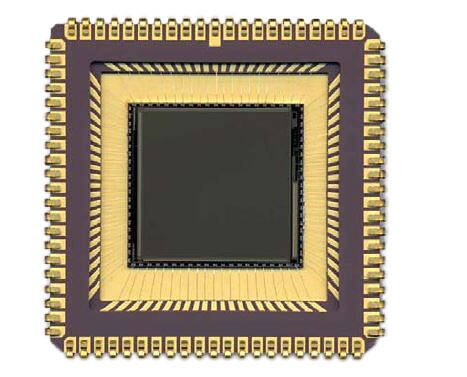
Figure 1. STAR250 Photograph
JLDCC84
CASE 114AK
Applications
• Applications Requiring Higher Pixel Pitch
• Scientific Applications Requiring Radiation
Tolerance
• Nuclear Inspection
Overview
The STAR250 sensor is a CMOS active pixel sensor featuring 512 x 512 pixels on a 25 mm pitch, on chip fixed pattern
noise (FPN) correction, a programmable gain amplifier, and a 10-bit ADC. Flexible operating (multiple windowing,
sub-sampling) is possible by direct addressable X and Y registers.
The sensor has an outstanding radiation tolerance that is observed using proprietary technology modifications and design
techniques. The STAR250 utilizes a BK7G18 glass lid with anti reflective coating. The cavity is filled with N2 increasing the
temperature operating range.
ORDERING INFORMATION
Marketing Part Number
Description
Package
NOIS1SM0250A-HHC
Mono with BK7G18 glass
84−pin JLCC
case 114AK
NOIS1SM0250A-WWC
Mono wafer
Wafer Sales
NOTE: Refer to Ordering Code Definition on page 2 for more information.
© Semiconductor Components Industries, LLC, 2014
January, 2017 − Rev. 11
1
Publication Order Number:
NOIS1SM0250A/D
�NOIS1SM0250A
ORDERING CODE DEFINITION
N O I S1 S M 0250 A − H H C
N = ON Semiconductor
O = Opto
Temperature Range
I = Image Sensors
H= BK7G18 Glass
STAR
H= JLCC
S = Standard Process
A= Engineering Model
M = Mono
0.25 MP Resolution
Marking
The marking shall consist of a lead identification and traceability information.
Lead Identification
An index to pin 1 shall be located on the top of the package as shown in section Package Dimensions on page 21. The pin
numbering is counter clock-wise, when looking at the top-side of the component.
Traceability Information Tests
Each component shall be marked such that complete traceability can be maintained.
The component shall bear a number that is constituted as follows:
Orderable Part Number
NOIS1SM0250A-HHC
Package Mark: Line 1
Package Mark: Line 2
NOIS1SM0250A
-HHC_NNNN
AWLYYWW
where NNNN- serialized number controlled manually by ON Semiconductor, BELGIUM
where AWLYYWW represents the lot assembly date
MARKING DIAGRAM
12
32
11
33
1
84
75
53
74
52
XXXXX
A
WL
YY
WW
NNNN
= Specific Device Code
= Assembly Location
= Wafer Lot
= Year
= Work Week
= Serial Number
www.onsemi.com
2
Package Mark: Line 3
�NOIS1SM0250A
SPECIFICATIONS
Table 1. GENERAL SPECIFICATIONS
Parameter
Pixel architecture
Specification
3 transistor active pixel
4 diodes per pixel
Pixel size
25 x 25 mm2
Resolution
512 x 512 pixels
Pixel rate
8 Mps
Shutter type
Electronic
Frame rate
29 full frames/second
Extended dynamic range
Remarks
Radiation-tolerant pixel design
4 photodiodes for improved MTF
Integration time is variable, steps equal to the row readout
time
Double slope
Programmable gain
Programmable between x1, x2, x4, x8
Supply voltage VDD
5V
Operational temperature
range
Package
–40°C to +85°C
Selectable through pins G0 and G1
Nitrogen in cavity
84-pin JLCC
Table 2. ELECTRO-OPTICAL SPECIFICATIONS
Parameter
Detector technology
Pixel structure
Photodiode
Specification (Typical)
CMOS active pixel sensor
3-transistor active pixel
4 diodes per pixel
Radiation-tolerant pixel design
4 photodiodes for improved MTF
High fill factor photodiode
Sensitive area format
512 by 512 pixels
Pixel size
25 mm2 x 25 mm2
Spectral range
Comment
200 nm to 1000 nm
See Figure 2 and Figure 3
Quantum efficiency x fill factor
Maximum 35%
Above 20% between 450 nm and 750 nm
(Metal FillFactor (MFF) is 63%)
Full well capacity
311K electrons
When output amplifier gain = 1
Linear range within +1%
128K electrons
When output amplifier gain = 1
1.68 V
When output amplifier gain = 1
Output signal swing
Conversion gain
Temporal noise
Dynamic range
FPN
PRNU (photo response
nonuniformity)
5.7 mV/e76
Dominated by kTC
74 dB (5000:1)
At the analog output
1 < 0.1% of full well
(typical)
Measured local, on central image area 50% of pixels in
the dark
Local: 1 = 0.39% of response
Global: 1 = 1.3% of response
Average dark current signal
4750 e-/s
DSNU (dark signal nonuniformity)
3805
e-/s
MTF
Horizontal: 0.36
Vertical: 0.39
Optical cross talk
When output amplifier gain = 1 near dark
e-
Measured in central image area 50% of pixels, at Qsat/2
At RT
RMS
At RT, scale linearly with integration time
at 600 nm.
5% to nearest neighbor if central pixel is
homogeneously illuminated
www.onsemi.com
3
�NOIS1SM0250A
Table 2. ELECTRO-OPTICAL SPECIFICATIONS
Parameter
Specification (Typical)
Antiblooming capacity
x 1000 to x 100 000
Output amplifier gain
1, 2, 4, or 8
Windowing
Controlled by two bits
X and Y 9-bit programmable shift registers
Electronic shutter range
1: 512
ADC
10-bit
±3.5 counts
Missing codes
none
ADC setup time
310 ns
ADC delay time
125 ns
Indicate upper left pixel of each window
Integration time is variable in time steps equal to the row
readout time
ADC linearity
Power dissipation
Comment
INL
To reach 99% of final value
< 350 mW
Average at 8 MHz pixel rate
Spectral Response Curve
Figure 2. Spectral Response Curve
www.onsemi.com
4
�NOIS1SM0250A
Figure 3. UV Region Spectral Response Curve
Pixel Profile
Figure 4. Pixel Profile
conditions are adjusted such that the transition covers 50%
of the output range. The scan is performed both horizontal
and vertical.
The pixel profile is measured using the ‘knife edge’
method: the image of a target containing a black to white
transition is scanned over a certain pixel with subpixel
resolution steps. The sensor settings and illumination
www.onsemi.com
5
�NOIS1SM0250A
Electrical Specifications
Absolute Maximum Ratings
Absolute ratings are those values beyond which damage to the device may occur.
Table 3. ABSOLUTE MAXIMUM RATINGS STAR250BK7
Characteristics
Units
Limits
Remarks
Min
Max
Any supply voltage
–0.5
+7
V
Voltage on any input terminal
–0.5
VDD + 0.5
V
Storage temperature
–40
+85
°C
–40
+120
°C
Maximum 1 hour
NA
125
°C
Hand soldering only. The sensor’s temperature
during soldering should not exceed this limit.
Sensor soldering temperature
Stresses exceeding those listed in the Maximum Ratings table may damage the device. If any of these limits are exceeded, device functionality
should not be assumed, damage may occur and reliability may be affected.
Table 4. RADIATION TOLERANCE
Parameter
Gamma total dose radiation
tolerance
Criterion
Qualification level
Increase in average dark current < 1 nA/cm2 after 3 MRad
See Figure 5
Image operation with dark signal < 1V/s
10 Mrad demonstrated (Co60)
Single (test) pixel operation with dark signal < 1V/s
Proton radiation tolerance
1% of pixels has an increase in dark current > 1
after 3 x 10^10 protons at 11.7 MeV
SEL threshold
> 80 MeV cm3 mg-1
nA/cm2
24 Mrad demonstrated (Co60)
See Figure 5
To be confirmed
www.onsemi.com
6
�NOIS1SM0250A
Figure 5 shows the increase in dark current under total dose irradiation. This curve is measured when the radiation is at high
dose rate. Annealing results in a significant dark current decrease.
Dark current increase [nA/cm
2
]
1,4
1,2
1
0,8
0,6
0,4
0,2
0
0
2
4
6
8
10
12
Total Ionizing Dos e [M r ad(Si)]
Figure 5. Dark Current Increase
Figure 6 shows the percentage of pixels with a dark current increase under 11.7 Mev radiation with protons.
Figure 6. Percentage of Pixels with Dark Current Increase
www.onsemi.com
7
�NOIS1SM0250A
DC Operating Conditions
Table 5. DC SPECIFICATIONS
Symbol
Parameter (Notes 1, 2 and 3)
Min
Typ
Max
Units
VDD_ANA
Analog supply voltage to imager part
–
5
–
V
VDD_DIG
Digital supply voltage to imager part
–
5
–
V
VDD_ADC_ANA
Analog supply voltage to ADC
–
5
–
V
VDD_ADC_DIG
Digital supply voltage to ADC
–
5
–
V
VDD_ADC_DIG_3.3/5
Supply voltage of ADC output stage
–
3.3 to 5
–
V
VIH
Logical ‘1’ input voltage
2.3
–
VDD
V
VIL
Logical ‘0’ input voltage
0
–
1
V
VOH
Logical ‘1’ output voltage
4.25
4.5
–
V
VOL
Logical ‘0’ output voltage
–
0.1
1
V
VDD_PIX
Pixel array power supply (default 5 V, the device is then
in ‘soft reset’. To avoid the image lag associated with
soft reset, reduce this voltage to 3–3.5 V ‘hard reset’)
–
5
–
V
VDD_RESL
Reset power supply
–
5
–
V
1. All parameters are characterized for DC conditions after establishing thermal equilibrium.
2. Unused inputs must always be tied to an appropriate logic level, for example, either VDD or GND.
3. This device contains circuitry to protect the inputs against damage due to high static voltages or electric fields. Take normal precautions to
avoid applying any voltages higher than the maximum rated voltages to this high impedance circuit.
www.onsemi.com
8
�NOIS1SM0250A
SENSOR ARCHITECTURE
Clk_YR
SyncYR
Sync_YL
9
Clk_YL
A8...A0
Col
Sel
Rst
D9...D0
10-bit ADC
9
Y Address
Decoder / Shift Register
9
512
Pixel Array
512 by 512 Pixels
Y Address
Decoder / Shift Register
Ld_Y
Y-Start Registeer-Decoder
10
512
Clk_ADC
Ain
512
S
Column Amplifiers
R
Rst
512
Sig
9
Progr. Gain
Amplifier
Aout
X-Start Register
X Address
Decoder / Shift Register
G0
G1
Blackref
Cal
Sync_X
CLKX
Ld_X
Figure 7. STAR250 Schematic
signal that is connected to the column bus by T3. The reset
and read entrance of the pixel are connected to one of the Y
shift registers.
The base line of the STAR250 sensor design consists of
an imager with a 512 by 512 array of active pixels at 25 mm
pitch. The detector contains on-chip correction for FPN in
the column amplifiers, a programmable gain output
amplifier, and a 10-bit ADC. Through additional preset
registers, the start position of a window can be programmed
to enable fast read out of only part of the detector array.
T1
Read
T2
Column Bus
Reset
Pixel Structure
The image sensor consists of several building blocks as
outlined in Figure 7. The central element is a 512 by 512
pixel array with square pixels at 25 mm pitch. Unlike
classical designs, the pixels of this sensor contain four
photodiodes. This configuration enhances the MTF and
reduces the PRNU. Figure 8 shows an electrical diagram of
the pixel structure. The four photodiodes are connected in
parallel to the reset transistor (T1). Transistor T2 converts
the charge, collected on the photo diode node, to a voltage
T3
Figure 8. STAR250 Pixel Structure
www.onsemi.com
9
�NOIS1SM0250A
Shift Registers
Electronic Shutter
The shift registers are located next to the pixel array and
contain equal number of outputs and pixel array rows. They
are designed as “1-hot” registers, (YL and YR shift register)
each allowing selection of one row of pixels at a time. A
clock pulse moves the pointer one position down the register
resulting in the selection of every individual row for either
reset or readout. The spatial offset between the two selected
rows determines the integration time. A synchronization
pulse to the shift registers loads the value from a preset
register into the shift register forcing the pointer to a
predetermined position. Windowing in the vertical (Y)
direction is achieved by presetting the registers to a row that
is not the first row and by clocking out only the required
number of rows.
In a linescan integrating imager with electronic shutter,
there are two continuous processes of image gathering.
The first process resets lines in a progressive scan. At line
reset, all the pixels in a line are drained from any photo
charges collected since their last reset or readout. After reset,
a new exposure cycle starts for that particular line.
The second process is the actual readout, which also
happens in an equally fast linewise progressive scan.
During readout, the photo charges collected since the
previous reset are converted into an output voltage. This is
then passed on pixel by pixel to the imager’s pixel serial
output and ADC. Readout is destructive, meaning the
accumulation of charges from successive exposure phases is
not possible in the present architecture.
The STAR250 has two Y shift registers; YL and YR. One
is used to read out a line (YL) and the other is used to reset
a line (YR). The integration time is equal to the time between
the last reset and readout of that line, see Figure 9. The
integration time is calculated as follows:
Integration time = (Nr. Lines * (RBT + pixel period * Nr.
Pixels)) with:
• Nr. Lines: Number of lines between readout and reset
(Y).
• Nr. Pixels: Number of pixels read out each line (X).
• RBT: Row Blanking Time = 3.2 ms (typical).
• Pixel period: 1/8 MHz = 125 ns (typical).
Column Amplifiers
All outputs from the pixels in a column are connected in
parallel to a column amplifier. This amplifier samples the
output voltage and the reset level of the pixel whose row is
selected at that moment and presents these voltage levels to
the output amplifier. As a result, the pixels are always reset
immediately after readout as part of the sample procedure
and the maximum integration time of a pixel is the time
between two read cycles.
x
Reset line
Read line
y
x
y
Line num ber
Reset sequence
Time axis
Integration time
Frame tim e
Figure 9. Electronic Shutter
www.onsemi.com
10
�NOIS1SM0250A
Programmable Gain Amplifier
The signal from the column amplifiers is fed to an output
amplifier with four presettable gains (adjustable with pins
G0 and G1). The offset correction of this amplifier is done
through a black reference procedure. The signal from the
output amplifier is externally available on the analog output
terminator of the device.
RADC_VHIGH
Pin 70: VHIGH_ADC
External
Internal
Analog-to-Digital Converter
RADC
The on-chip 10-bit ADC is electrically separated from the
other circuits of the device. The ADC conversion range is set
by the voltages on VLOW_ADC (pin 47) and
VHIGH_ADC (pin 70). Make voltages on these pins equal
to about 2 V on VLOW_ADC and 4 V on VHIGH_ADC.
The voltages are set by connecting VLOW with 1.2 kW to
GND and VHIGH_ADC with 560 W to VDD. This way, a
resistor ladder is created as shown in Figure 10.
Pin 47: VLOW_ADC
External
RADC_VLOW
Figure 10. ADC Resistor Ladder
The internal ADC resistance varies according to
temperature. The resistance value increases approximately
4.4 W/°C with increasing temperature. If the ADC range is
set externally with resistors, the conversion range may vary
with temperature. This effect is cancelled out by not making
use of resistors but directly applying voltages on
VLOW_ADC and VHIGH_ADC.
TIMING AND READOUT OF IMAGE SENSOR
Image Readout Procedure
♦
A preamble or initialization phase is irrelevant. The
sensor is read out continuously. The first frame is generally
saturated and useless because there is no preceding reset of
each pixel.
Image Readout
In an infinite uninterrupted loop, follow these steps for
every line:
1. Synchronize the read (YL) and/or reset (YR)
registers:
♦ SYNC_YL - to reinitiate the readout sequence to
row position Y1
♦ SYNC_YR - to reinitiate the reset pointer to row
position Y1
For all other lines do not pulse one of these SYNC_Y
signals.
2. Operate the double sampling column amplifiers with
two RESETs. Apply one to reset the line that is
currently selected to produce the reset reference level
for the double sampling column amplifiers. Apply the
other reset to another line depending on the required
integration time reduction.
3. Perform a line readout:
♦ Reset the X read address shift register to the value in
its shadow register (X1).
♦ Perform a pixel readout operation, operating the
track/hold and the ADC.
♦
Shift the X read address shift register one position
further.
Shift the Y read and reset address shift registers one
position further. If either of Y read or reset address
shift register comes to the end of the pixel array (or
the ROI), wrap it around to the start position by
pulsing SYNC_YL.
Readout Timing
The actual line readout process starts with addressing the
line to read. This is done either by initializing the YL pointer
with a new value or by shifting it one position beyond its
previous value. (Addressing the line has reset, YR is done in
an analogous fashion). During the “blanking time”, after the
new line is addressed on the sensor, the built-in
column-parallel double sampling amplifiers are operated.
This renders offset-corrected values of the line under
readout.
After the blanking time, the pixels of the row addressed by
YL are read by multiplexing all the pixels one by one to the
serial output chain. The pixel is selected by the X pointer and
that pointer is either initialized with a new value or an
increment of the previous position.
The time between row resets and their corresponding row
readouts is the effective exposure time (or integration time).
This time is proportional to the number of lines
(DelayLines) between the line currently under reset and the
line currently under readout: DelayLines = (YR - YL+1).
www.onsemi.com
11
�NOIS1SM0250A
May occur at any moment,
persumably once per
sequence of frames
Once per frame
This time is also equal to the delay between the SYNC_YR
pulse and the subsequent SYNC_YR.
The effective integration time tint is calculated as
delaylines x line time. The line time is a function of four
terms: the time to output the desired number of pixels in the
line (Wframe) and the overhead (“blanking”) time needed to
select a new line and perform the double sampling and reset
operations.
T13
T10
CAL
T2
T9
T16
Row Start
Address
T15
T17
LD_Y
T14
T12
T1
S
T3
T7
RESET
T4
T4
T6
R
T11
T5
L/R
T8
Row
Y-�1
Row Blanking Time
Time Available for Read Out of Row Y
Figure 11. Basic Readout Timing
first row. CAL is pulsed on the first row too, 2 ms later than
SYNC_YL.
The minimal idle time is 1.4 ms (before starting reading
pixels). However, do not read out pixels during the complete
row initialization process (in between the rising edge on S
and the falling edge on L/R). In this case, the total idle time
is minimal. This timing assumes that the Y start register was
loaded in advance, which can occur at any time but before
the pulse on SYNC_YL or SYNC_YR.
SYNC_YR is not identical to SYNC_YL. SYNC_YR is
used in electronic shutter operation. The CLK_YR is driven
identical to CLK_YL, but the SYNC_YR pulse leads the
SYNC_YL pulse by a certain number of rows. This lead
time is the effective integration (electronic shutter ~) time.
Relative to the row timing, both SYNC pulses are given at
the same time position, once for each frame, but during
different rows.
SYNC_YL is pulsed when the first row is read out and
SYNC_YR is pulsed for the electronic shutter to start for this
www.onsemi.com
12
�NOIS1SM0250A
Table 6. READOUT TIMING SPECIFICATIONS
Symbol
Min
Typ
T1
1.8 ms
–
Delay between selection of new row by falling edge on CLK_YL and falling edge on S.
Minimal value. Normally, CLK_YR is low already at the end of the previous sequence.
Description
T2
1.8 ms
–
Delay between selection of new a row by SYNC_YL and falling edge on S.
T3
0.4 ms
–
Duration of S and R pulse.
T4
0.1 ms
–
Duration of RESET pulse.
T5
T4 + 40 ns
0.3 ms
T6
0.8 ms
–
Delay between falling edge on RESET and falling edge on R.
T7
20 ns
0.1 ms
Delay between falling edge on S and rising edge on RESET.
T8
0
1 ms
Delay between falling edge on L/R and falling edge on CLK_Y.
T9
100 ns
1 ms
Duration of cal pulse. The CAL pulse is given once each frame.
T10
0
2 ms
Delay between falling edge of SYNC_YL and rising edge of CAL pulse.
L/R pulse must overlap second RESET pulse at both sides.
T11
40 ns
0.1 ms
T12
0.1 ms
1 ms
Delay between falling edge on R and rising edge on L/R.
T13
–
0.5 ms
Pulse width SYNC_YL/YR.
T14
–
0.5 ms
Pulse width CLK_YL/YR.
T15
10 ns
–
Address setup time.
T16
20 ns
–
Load X/Y start register value.
T17
10 ns
–
Address stable after load.
T18
10 ns
–
T19
20 ns
–
T20
10 ns
–
T21
–
40 ns
Analog output is stable during CLK_X low.
T22
–
40 ns
CLK_X pulse width: During this clock phase the analog output ramps to the next pixel level.
T23
–
125 ns
ADC digital output stable after falling edge of CLK_ADC.
Delay between rising edge of CLK_Y and falling edge on S.
SYNC_X pulse width. SYNC_X while CLK_X is high.
Loading the X and Y Start Positions
The following timing constraints apply:
Load the X or Y start addresses in advance, before the X
or Y shift registers are preset by a SYNC pulse. However, if
necessary, they can be loaded just before the SYNC_X or
SYNC_Y pulse as shown in Figure 12.
For example, the X start register can be loaded during the
row idle time. The Y start register can be loaded during
readout of the last row of the previous frame.
If the X or Y start address does not change for later frames,
it does not need to be reloaded in the register.
The start positions (start addresses) for region of interest
(ROI) are preloaded in the X or Y start register. They become
effective by the application of the SYNC_X, SYNC_YL
and/or SYNC_YR. The start X or Y address must be applied
to their common address bus and the corresponding LD_X
or LD_Y pin must be pulsed.
On each falling edge of CLK_X, a new pixel of the same
row (line) is accessed. The output stage is in hold when
CLK_X is low and starts generating a new output after a
rising edge on CLK_X.
www.onsemi.com
13
�NOIS1SM0250A
May Occur at any
Moment in Time
Row Blanking Time
Time Available for Read Out of Row Y
Column Start
Address
T15������ T17
LD_X
T16
T19
SYNC_X
CLK_X
T18��T20
Analog
Output
T21
T22
Pixel 1
Pixel 2
Pixel 3
CLK ADC
T23
Pixel 1
ADC Out
Pixel 2
Figure 12. Timing to Load X and Y Registers
Other Signals
TESTDIODE
and
TESTPIXEL_ARRAY
are
connections to optical test structures that are used for electro
optical evaluation. TESTDIODE is a plain photodiode with
an area of 14 x 5 pixels. TESTPIXEL_ARRAY is an array
(14 x 5) of pixels where the photodiodes are connected in
parallel. These structures measure the photocurrent of the
diodes directly.
TESTPIXEL_RESET and TESTPIXEL-OUT are
connections to a single pixel that are used for testing.
Tie SELECT signal to VDD for normal operation. This
signal is added for diagnostic reasons and inhibits the pixel
array operation when held low.
The CAL signal sets the output amplifier DC offset level.
When this signal is active (high) the pixel array is internally
disconnected from the output amplifier, its gain is set to
unity and its input signal is connected to the BLACK_REF
input. Perform this action at least once for each frame.
EOS_X, EOS_YL, and EOS_YR produce a pulse when
the respective shift register comes at its end. These outputs
are used mainly during testing to verify proper operation of
the shift registers.
www.onsemi.com
14
�NOIS1SM0250A
PIN LIST
Table 7. POWER SUPPLY CONNECTIONS
Pin
Pin Name
Pin Description
10
VDD_ANA
Analog power supply 5 V
11
VDD_DIG
Digital power supply 5 V
31
VDD_AMP
Power supply of output amplifier 5 V
33
VDD_DIG
Digital power supply 5 V
34
VDD_ANA
Analog power supply 5 V
49
VDD_RESR
Reset power supply 5 V
50
VDD_DIG
Digital power supply 5 V
53
VDD_ADC_ANA
ADC analog power supply 5 V
66
VDD_ADC_ANA
ADC analog power supply 5 V
67
VDD_ADC_DIG
ADC digital power supply 5 V
69
VDD_ADC_DIG_3.3/5
52
76
VDD_PIX
Pixel array power supply [default: 5 V, the device is then in ‘soft reset’. To avoid the image
lag associated with soft reset, reduce this voltage to 3…3.5 V ‘hard reset’]
78
VDD_DIG
Digital power supply 5 V
79
VDD_RESL
Reset power supply 5 V
ADC 3.3 V power supply for digital output of ADC
For interface with 5 V external system: connect to VDD_ADC_DIG
For interface with 3.3 V external system: connect to 3.3 V power supply
Table 8. GROUND CONNECTIONS
Pin
Pin Name
Pin Description
9
GND_ANA
Analog ground
12
GND_DIG
Digital ground
30
GND_AMP
Ground of output amplifier
32
GND_DIG
Digital ground
35
GND_ANA
Analog ground
51
GND_DIG
Digital ground
54
GND_ADC_ANA
ADC analog ground
65
GND_ADC_ANA
ADC analog ground
68
GND_ADC_DIG
ADC digital ground
77
GND_DIG
Digital ground
Table 9. DIGITAL INPUT SIGNALS
Pin
Pin Name
Pin Description
1
S
Control signal for column amplifier
Apply pulse pattern; see Figure 11.
2
R
Control signal for column amplifier
Apply pulse pattern; see Figure 11.
3
RESET
Resets row indicated by left/right shift register
high active (1= reset row)
Apply pulse pattern; see Figure 11.
4
SELECT
Selects row indicated by left/right shift register
high active (1=select row)
Apply 5 V DC for normal operation
www.onsemi.com
15
�NOIS1SM0250A
Table 9. DIGITAL INPUT SIGNALS
Pin
Pin Name
Pin Description
5
L/R
Use left or right shift register for SELECT and RESET
1 = left / 0 = right; see Figure 11.
6
A0
Start address for X and Y pointers (LSB)
7
A1
Start address for X and Y pointers
8
A2
Start address for X and Y pointers
13
A3
Start address for X and Y pointers
14
A4
Start address for X and Y pointers
15
A5
Start address for X and Y pointers
16
A6
Start address for X and Y pointers
17
A7
Start address for X and Y pointers
18
A8
Start address for X and Y pointers (MSB)
19
LD_Y
Latch address (A0…A8) to Y start register (0 = track, 1 = hold)
20
LD_X
Latch address (A0…A8) to X start register (0 = track, 1 = hold)
21
CLK_YL
22
SYNC_YL
Clock YL shift register (shifts on falling edge)
Sets YL shift register to location preloaded in Y start register
Low active (0=sync)
Apply SYNC_YL when CLK_YL is high
24
CLK_X
Clock X shift register (output valid and s when CLK_X is low)
25
SYNC_X
Sets X shift register to location preloaded in X start register
Low active (0=sync)
Apply SYNC_X when CLK_X is high
After SYNC_X, apply falling edge on CLK_X, and rising edge on CLK_X
27
CLK_YR
Clock YR shift register (shifts on falling edge)
28
SYNC_YR
36
CAL
37
G0
Select output amplifier gain value: G0 = LSB; G1 = MSB
00 = unity gain; 01 = x2; 10 = x4; 11 = x8
38
G1
idem
71
CLK_ADC
ADC clock
ADC converts on falling edge
75
BITINVERT
1 = invert output bits
0 = no inversion of output bits
80
TRI_ADC
Sets YR shift register to location preloaded in Y start register
Low active (0=sync)
Apply SYNC_YR when CLK_YR is high
Initialize output amplifier
Output amplifier will output BLACKREF in unity gain mode when CAL is high (1)
Apply pulse pattern (one pulse per frame); see Figure 11.
Tristate control of digital ADC outputs
1 = tristate; 0 = output
www.onsemi.com
16
�NOIS1SM0250A
Table 10. DIGITAL OUTPUT SIGNALS
Pin
Pin Name
23
EOS_YL
End-of-scan of YL shift register
Low first clock period after last row (low active)
Pin Description
26
EOS_X
End-of-scan of X shift register
Low first clock period after last active column (low active)
29
EOS_YR
55
D0
ADC output bit (LSB)
56
D1
ADC output bit
57
D2
ADC output bit
58
D3
ADC output bit
59
D4
ADC output bit
60
D5
ADC output bit
61
D6
ADC output bit
62
D7
ADC output bit
63
D8
ADC output bit
64
D9
ADC output bit (MSB)
End-of-scan of YR shift register
Low first clock period after last row (low active)
Table 11. ANALOG INPUT SIGNALS
Pin
Pin Name
Pin Description
39
NBIASARR
40
PBIAS
41
NBIAS_AMP
Output amplifier speed/power control.
Connect with 51 kW to VDD and decouple with 100 nF to GND for 8 MHz output rate (Lower
resistor values yield higher maximal pixel rates at the cost of extra power dissipation).
42
BLACKREF
Control voltage for output signal offset level.
Buffered on-chip, the reference level can be generated by a 100 kW resistive divider.
Connect to ± 2 V DC for use with on-chip ADC.
44
IN_ADC
45
NBIASANA2
Connect with 100 k to VDD and decouple to GND.
46
NBIASANA
Connect with 100 k to VDD and decouple to GND.
47
70
VLOW_ADC
VHIGH_ADC
48
G_AB
Connect with 470 k to VDD and decouple to ground with a 100 nF capacitor.
Connect with 39 k to ground and decouple to VDD with a 100 nF capacitor for 8 MHz pixel
rate. (Lower resistor values yield higher maximal pixel rates at the cost of extra power dissipation).
Input, connect to sensor output.
Input range is between 2 and 4 V (VLOW_ADC and VHIGH_ADC).
Low reference and high reference voltages of ADC should be about 2 V and 4 V.
The required voltage settings on VLOW_ADC and VHIGH_ADC can be approximated by
tying VLOW_ADC with 1.2 kW to GND and VHIGH_ADC with 560 W to VDD.
Antiblooming drain control voltage:
Default: connect to ground. The antiblooming is operational but not maximal.
Apply 1 V DC for improved antiblooming.
72
PBIASDIG2
Connect with 100 K to GND and decouple to VDD.
73
PBIASENCLOAD
Connect with 100 K to GND and decouple to VDD.
74
PBIASDIG1
Connect with 47 K to GND and decouple to VDD.
Table 12. ANALOG OUTPUT SIGNALS
Pin
Pin Name
43
OUT
Pin Description
Analog output signal are connected to the analog input of the ADC.
www.onsemi.com
17
�NOIS1SM0250A
Table 13. TEST STRUCTURES
Pin
Pin Name
81
TESTDIODE
82
TESTPIX
ARRAY
83
TESTPIXEL_RESET
84
TESTPIXEL_OUT
Pin Description
Plain photo diode, size: 14 x 25 pixels.
Must be left open for normal operation.
Array of test pixels, connected in parallel (14 x 25 pixels).
Must be left open for normal operation.
Reset input of single test pixel.
Must be tied to GND for normal operation.
Output of single test pixel.
Must be left open for normal operation.
Glass Lid Specifications
Figure 13. Geometrical Characteristics (in mm)
www.onsemi.com
18
�NOIS1SM0250A
Table 15. MECHANICAL SPECIFICATIONS
Limits
Min
Typ
Max
Units
–
–
0.15
mm
Die position, X offset
–0.05
0
0.05
mm
Die position, Y offset
–0.018
–
0.118
mm
Die position, planarity
–0.05
0
0.05
mm
Die position, Y tilt
–0.05
0
0.05
mm
Characteristics
Package tolerance
NOTE: Min and Max limits are not measured on every unit, but guaranteed by assembly process.
Die Alignment
The die is aligned manually in the package to a tolerance of ±50 mm and the alignment is verified after hardening the die
adhesive. All dimensions in Figure 14 are in mm.
Parallelism in
X and Y within
+ 50 μm
68 μ
Pin 1
Center of Cavity
and of FPA
Center of
Silicium
A
Bonding Cavity:
0.508+0.051
Offset Between Center of
Silicium and Center of
Cavity:
X: 0
Y: 68 μm
Die:
0.508+0.01
Die Cavity:
0.508+0.051
A
Glass Window:
1.0+/-0.05
Window Adhesive:
0.08+0.02
A-
Die Adhesive:
0.08+0.02
Section A
Drawing Not to Scale
Figure 14. Die Alignment
www.onsemi.com
19
�NOIS1SM0250A
ADDITIONAL REFERENCES AND RESOURCES
Application Notes and other resources can be found
linked to the product web page at www.onsemi.com.
Additional information on this device may also be available
in the Image Sensor Portal, accessible within the MyON
section of www.onsemi.com. A signed NDA is required to
access the Image Sensor Portal – please see your
ON Semiconductor sales representative for more
information.
For quality and reliability information, please download
the Quality & Reliability Handbook (HBD851/D) from
www.onsemi.com.
For information on Standard terms and Conditions of
Sale, please download Terms and Conditions document
from www.onsemi.com.
For information on Return Material Authorization
procedures, please refer to the RMA Policy Procedure
document from www.onsemi.com.
The Product Acceptance Criteria document, which lists
criteria to which this device is tested prior to shipment, is
available upon request.
For information on ESD and cover glass care and
cleanliness, please download the Application Note Image
Sensor Handling and Best Practices (AN52561/D) from
www.onsemi.com.
www.onsemi.com
20
�NOIS1SM0250A
ACRONYMS
Acronym
Definition
Acronym
Definition
ADC
analog to digital convertor
MBPS
megabit per second
CIS
CMOS image sensor
MCIS
multifield point CMOS image sensor
CMOS
complementary metal oxide semiconductor
MFF
metal fill factor
CY
Cypress
MIM
metal-insulator-metal
DC
dark current
MP
megapixel
DNL
differential nonlinearity
Mrad
megaradiation
DS
double sampling
MSB
most significant bit
DSNU
dark signal nonuniformity
MSPS
megasamples per second
ESD
electrostatic discharge
MTF
modulation transfer function
FF
fill factor
MUX
multiplexer
FPN
fixed pattern noise
PCB
printed circuit board
FPS
frames per second
PLL
phase-locked loop
FS
frame start
PLS
parasitic light sensitivity
fs
full scale
PRBS
pseudo random bit stream
I/O
input/output
PRNU
photo response nonuniformity
IMG
image
PSN
photon shot noise
INL
integral nonlinearity
PSNL
pixel storage node leakage
IP
intellectual property
QC
quantum conversion
LDO
low drop-out
QE
quantum efficiency
LSB
least significant bit
QFW
pixel full-well charge
LVDS
low voltage differential signaling
RMS
root mean square
MBS
mixed boundary scan
ROI
region of interest
www.onsemi.com
21
�NOIS1SM0250A
GLOSSARY
conversion gain
A constant that converts the number of electrons collected by a pixel into the voltage swing of the pixel. Conversion gain = q/C where q is the charge of an electron (1.602E 19 Coulomb) and C is the capacitance of the
photodiode or sense node.
DNL
Differential nonlinearity (for ADCs)
DSNU
Dark signal nonuniformity. This parameter characterizes the degree of nonuniformity in dark leakage currents,
which can be a major source of fixed pattern noise.
fill-factor
A parameter that characterizes the optically active percentage of a pixel. In theory, it is the ratio of the actual
QE of a pixel divided by the QE of a photodiode of equal area. In practice, it is never measured.
INL
Integral nonlinearity (for ADCs)
IR
Infrared. IR light has wavelengths in the approximate range 750 nm to 1 mm.
Lux
Photometric unit of luminance (at 550 nm, 1lux = 1 lumen/m2 = 1/683 W/m2)
pixel noise
Variation of pixel signals within a region of interest (ROI). The ROI typically is a rectangular portion of the pixel
array and may be limited to a single color plane.
photometric units
Units for light measurement that take into account human physiology.
PLS
Parasitic light sensitivity. Parasitic discharge of sampled information in pixels that have storage nodes.
PRNU
Photo-response nonuniformity. This parameter characterizes the spread in response of pixels, which is a
source of FPN under illumination.
QE
Quantum efficiency. This parameter characterizes the effectiveness of a pixel in capturing photons and converting them into electrons. It is photon wavelength and pixel color dependent.
read noise
Noise associated with all circuitry that measures and converts the voltage on a sense node or photodiode into
an output signal.
reset
The process by which a pixel photodiode or sense node is cleared of electrons. ”Soft” reset occurs when the
reset transistor is operated below the threshold. ”Hard” reset occurs when the reset transistor is operated
above threshold.
reset noise
Noise due to variation in the reset level of a pixel. In 3T pixel designs, this noise has a component (in units of
volts) proportionality constant depending on how the pixel is reset (such as hard and soft). In 4T pixel designs, reset noise can be removed with CDS.
responsivity
The standard measure of photodiode performance (regardless of whether it is in an imager or not). Units are
typically A/W and are dependent on the incident light wavelength. Note that responsivity and sensitivity are
used interchangeably in image sensor characterization literature so it is best to check the units.
ROI
Region of interest. The area within a pixel array chosen to characterize noise, signal, crosstalk, and so on.
The ROI can be the entire array or a small subsection; it can be confined to a single color plane.
sense node
In 4T pixel designs, a capacitor used to convert charge into voltage. In 3T pixel designs it is the photodiode
itself.
sensitivity
A measure of pixel performance that characterizes the rise of the photodiode or sense node signal in Volts
upon illumination with light. Units are typically V/(W/m2)/sec and are dependent on the incident light wavelength. Sensitivity measurements are often taken with 550 nm incident light. At this wavelength, 1 683 lux is
equal to 1 W/m2; the units of sensitivity are quoted in V/lux/sec. Note that responsivity and sensitivity are used
interchangeably in image sensor characterization literature so it is best to check the units.
spectral response
The photon wavelength dependence of sensitivity or responsivity.
SNR
Signal-to-noise ratio. This number characterizes the ratio of the fundamental signal to the noise spectrum up
to half the Nyquist frequency.
temporal noise
Noise that varies from frame to frame. In a video stream, temporal noise is visible as twinkling pixels.
www.onsemi.com
22
�MECHANICAL CASE OUTLINE
PACKAGE DIMENSIONS
JLDCC84
CASE 114AK−01
ISSUE O
DATE 06 JUL 2011
GENERIC MARKING DIAGRAM AND
SOLDER FOOTPRINT ON PAGE 2
DOCUMENT NUMBER:
STATUS:
98AON56453E
ON SEMICONDUCTOR STANDARD
REFERENCE:
© Semiconductor Components Industries, LLC, 2002
October, DESCRIPTION:
2002 − Rev. 0
JLDCC84
http://onsemi.com
1
Electronic versions are uncontrolled except when
accessed directly from the Document Repository. Printed
versions are uncontrolled except when stamped
“CONTROLLED COPY” in red.
Case Outline Number:
PAGE 1 OFXXX
3
�JLDCC84
CASE 114AK−01
ISSUE O
DATE 06 JUL 2011
GENERIC
MARKING DIAGRAM
XXXXX
A
WL
YY
WW
NNNN
DOCUMENT NUMBER:
STATUS:
98AON56453E
ON SEMICONDUCTOR STANDARD
REFERENCE:
© Semiconductor Components Industries, LLC, 2002
October, DESCRIPTION:
2002 − Rev. 0
JLDCC84
http://onsemi.com
2
= Specific Device Code
= Assembly Location
= Wafer Lot
= Year
= Work Week
= Serial Number
Electronic versions are uncontrolled except when
accessed directly from the Document Repository. Printed
versions are uncontrolled except when stamped
“CONTROLLED COPY” in red.
Case Outline Number:
PAGE 2 OFXXX
3
�DOCUMENT NUMBER:
98AON56453E
PAGE 3 OF 3
ISSUE
O
REVISION
RELEASED FOR PRODUCTION FROM CYPRESS DRAWING #001−07592 TO ON
SEMICONDUCTOR. REQ. BY K. BERKMAN.
DATE
06 JUL 2011
ON Semiconductor and
are registered trademarks of Semiconductor Components Industries, LLC (SCILLC). SCILLC reserves the right to make changes without further notice
to any products herein. SCILLC makes no warranty, representation or guarantee regarding the suitability of its products for any particular purpose, nor does SCILLC assume any liability
arising out of the application or use of any product or circuit, and specifically disclaims any and all liability, including without limitation special, consequential or incidental damages.
“Typical” parameters which may be provided in SCILLC data sheets and/or specifications can and do vary in different applications and actual performance may vary over time. All
operating parameters, including “Typicals” must be validated for each customer application by customer’s technical experts. SCILLC does not convey any license under its patent rights
nor the rights of others. SCILLC products are not designed, intended, or authorized for use as components in systems intended for surgical implant into the body, or other applications
intended to support or sustain life, or for any other application in which the failure of the SCILLC product could create a situation where personal injury or death may occur. Should
Buyer purchase or use SCILLC products for any such unintended or unauthorized application, Buyer shall indemnify and hold SCILLC and its officers, employees, subsidiaries, affiliates,
and distributors harmless against all claims, costs, damages, and expenses, and reasonable attorney fees arising out of, directly or indirectly, any claim of personal injury or death
associated with such unintended or unauthorized use, even if such claim alleges that SCILLC was negligent regarding the design or manufacture of the part. SCILLC is an Equal
Opportunity/Affirmative Action Employer. This literature is subject to all applicable copyright laws and is not for resale in any manner.
© Semiconductor Components Industries, LLC, 2011
July, 2011 − Rev. 01O
Case Outline Number:
114AK
�onsemi,
, and other names, marks, and brands are registered and/or common law trademarks of Semiconductor Components Industries, LLC dba “onsemi” or its affiliates
and/or subsidiaries in the United States and/or other countries. onsemi owns the rights to a number of patents, trademarks, copyrights, trade secrets, and other intellectual property.
A listing of onsemi’s product/patent coverage may be accessed at www.onsemi.com/site/pdf/Patent−Marking.pdf. onsemi reserves the right to make changes at any time to any
products or information herein, without notice. The information herein is provided “as−is” and onsemi makes no warranty, representation or guarantee regarding the accuracy of the
information, product features, availability, functionality, or suitability of its products for any particular purpose, nor does onsemi assume any liability arising out of the application or use
of any product or circuit, and specifically disclaims any and all liability, including without limitation special, consequential or incidental damages. Buyer is responsible for its products
and applications using onsemi products, including compliance with all laws, regulations and safety requirements or standards, regardless of any support or applications information
provided by onsemi. “Typical” parameters which may be provided in onsemi data sheets and/or specifications can and do vary in different applications and actual performance may
vary over time. All operating parameters, including “Typicals” must be validated for each customer application by customer’s technical experts. onsemi does not convey any license
under any of its intellectual property rights nor the rights of others. onsemi products are not designed, intended, or authorized for use as a critical component in life support systems
or any FDA Class 3 medical devices or medical devices with a same or similar classification in a foreign jurisdiction or any devices intended for implantation in the human body. Should
Buyer purchase or use onsemi products for any such unintended or unauthorized application, Buyer shall indemnify and hold onsemi and its officers, employees, subsidiaries, affiliates,
and distributors harmless against all claims, costs, damages, and expenses, and reasonable attorney fees arising out of, directly or indirectly, any claim of personal injury or death
associated with such unintended or unauthorized use, even if such claim alleges that onsemi was negligent regarding the design or manufacture of the part. onsemi is an Equal
Opportunity/Affirmative Action Employer. This literature is subject to all applicable copyright laws and is not for resale in any manner.
PUBLICATION ORDERING INFORMATION
LITERATURE FULFILLMENT:
Email Requests to: orderlit@onsemi.com
onsemi Website: www.onsemi.com
◊
TECHNICAL SUPPORT
North American Technical Support:
Voice Mail: 1 800−282−9855 Toll Free USA/Canada
Phone: 011 421 33 790 2910
Europe, Middle East and Africa Technical Support:
Phone: 00421 33 790 2910
For additional information, please contact your local Sales Representative
�