NP-SDMC Series
High Current TSPD
The NP−SDMC series of High Current Thyristor Surge Protection
Devices (TSPD) protect sensitive electronic equipment from transient
overvoltage conditions. The high current withstand of these devices
offer protection in extreme environments and provide a solution for
GR−1089 balanced “Y” configurations.
The NP−SDMC Series helps designers to comply with the various
regulatory standards and recommendations including:
GR−1089−CORE, IEC 61000−4−5, ITU K.20/K.21/K.45, IEC 60950,
TIA−968−A, FCC Part 68, EN 60950, UL 1950.
Features
•
•
•
•
http://onsemi.com
HIGH CURRENT (200A)
BIDIRECTIONAL SURFACE
MOUNT THYRISTOR
Low Leakage (Transparent)
High Surge Current Capabilities
Precise Turn on Voltages
These are Pb−Free Devices
T
R
Typical Applications
• Central Office
• Rugged Modems
• Bottom Element in “Y” Configurations
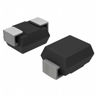
SMB
JEDEC DO−214AA
CASE 403C
ELECTRICAL CHARACTERISTICS
VDRM
V(BO)
CO, 2 V,
1 MHz
CO, 50 V,
1 MHz
MARKING DIAGRAM
V
V
pF (Max)
pF (Max)
NP0720SDMCT3G
65
88
65
30
NP1300SDMCT3G
120
160
65
30
AYWW
xxxDMG
G
NP1500SDMCT3G
140
180
65
30
NP1800SDMCT3G
170
220
65
30
NP3100SDMCT3G
275
350
65
30
Device
G in part number indicates RoHS compliance
Other protection voltages are available upon request
Symmetrical Protection − Values the same in both negative and positive excursions
(See V−I Curve on page 3)
A
Y
WW
xxx
= Assembly Location
= Year
= Work Week
= Specific Device Code
(NPxxx0SDMC)
G
= Pb−Free Package
(Note: Microdot may be in either location)
ORDERING INFORMATION
Device
Package
Shipping†
NPxxxxSDMCT3G
SMB
(Pb−Free)
2500 Tape &
Reel
†For information on tape and reel specifications,
including part orientation and tape sizes, please
refer to our Tape and Reel Packaging Specifications
Brochure, BRD8011/D.
© Semiconductor Components Industries, LLC, 2009
August, 2009 − Rev. 0
1
Publication Order Number:
NP3100SD/D
�NP−SDMC Series
MAXIMUM RATINGS (TA = 25°C unless otherwise noted)
Symbol
VDRM
IPPS
ITSM
Rating
Value
Unit
NP0720SDMCT3G
$65
V
NP1300SDMCT3G
$120
NP1500SDMCT3G
$140
NP1800SDMCT3G
$170
NP3100SDMCT3G
$275
Nonrepetitive peak pulse current: Rated maximum
value of peak impulse pulse current that may be
applied.
2x10 ms, GR−1089−CORE
1000
10x1000 ms, GR−1089−CORE
200
Non−repetitive peak on−state current: Rated
maximum (peak) value of ac power frequency
on−state surge current which may be applied for a
specified time or number of ac cycles.
0.0167s, 50/60 Hz, full sine wave
60
Repetitive peak off−state voltage: Rated maximum
(peak) continuous voltage that may be applied in the
off−state conditions including all dc and repetitive
alternating voltage components.
0.1s, 50/60 Hz, full sine wave
30
1000s, 50/60 Hz, full sine wave
2.2
A
A
Stresses exceeding Maximum Ratings may damage the device. Maximum Ratings are stress ratings only. Functional operation above the
Recommended Operating Conditions is not implied. Extended exposure to stresses above the Recommended Operating Conditions may affect
device reliability.
ELECTRICAL CHARACTERISTICS TABLE (TA = 25°C unless otherwise noted)
Symbol
V(BO)
I(BO)
IH
IDRM
VT
Rating
Min
Breakover voltage: The maximum voltage across the device in or at the
breakdown region.
VDC = 1000 V, dv/dt = 100 V/ms
Typ
Max
Unit
NP0720SDMCT3G
$88
V
NP1300SDMCT3G
$160
NP1500SDMCT3G
$180
NP1800SDMCT3G
$220
NP3100SDMCT3G
$350
Breakover Current: The instantaneous current flowing at the breakover voltage.
Holding Current: The minimum current required to maintain the device in the on−state.
Off−state Current: The dc value of current that results from the application of the off−state voltage
800
150
mA
VD = 50 V
2
VD = VDRM
5
On−state Voltage: The voltage across the device in the on−state condition.
IT = 2.2 A (pk), PW = 300 ms, DC = 2%
dv/dt
Critical rate of rise of off−state voltage: The maximum rate of rise of voltage (below VDRM) that
will not cause switching from the off−state to the on−state.
Linear Ramp between 0.1 VDRM and 0.9 VDRM
di/dt
Critical rate of rise of on−state current: rated value of the rate of rise of current which the device
can withstand without damage.
CO
Off−state Capacitance
f = 1.0 MHz, Vd = 1.0 VRMS, VD = −2 Vdc
mA
4
±5
mA
V
kV/ms
±500
A/ms
65
pF
THERMAL CHARACTERISTICS
Symbol
TSTG
TJ
R0JA
Rating
Value
Unit
Storage Temperature Range
−65 to +150
°C
Operating Temperature Range
−40 to +150
°C
90
°C/W
Thermal Resistance: Junction−to−Ambient Per EIA/JESD51−3, PCB = FR4 3”x4.5”x0.06”
Fan out in a 3x3 inch pattern, 2 oz copper track.
http://onsemi.com
2
�+I
ELECTRICAL PARAMETER/RATINGS DEFINITIONS
Symbol
Parameter
VDRM
Repetitive Peak Off−state Voltage
V(BO)
Breakover Voltage
IDRM
Off−state Current
I(BO)
Breakover Current
IH
Holding Current
VT
On−state Voltage
IT
On−state Current
ITSM
Nonrepetitive Peak On−state Current
IPPS
Nonrepetitive Peak Impulse Current
VD
Off−state Voltage
ID
Off−state Current
IPPS
ITSM
IT
On−State Region
NP−SDMC Series
I(BO)
VT
Off−State Region
IH
ID
−Voltage
VD
IDRM
V(BO)
VDRM
+Voltage
−I
Figure 1. Voltage Current Characteristics of TSPD
Ipp − PEAK PULSE CURRENT − %Ipp
PEAK ON−STATE CURRENT
100
10
1
0.1
1
10
100
CURRENT DURATION (s)
tr = rise time to peak value
tf = decay time to half value
Peak
Value
100
Half Value
50
0
1000
0 tr
tf
TIME (ms)
Figure 2. Nonrepetitive On−State Current vs. Time
(ITSM)
Figure 3. Nonrepetitive On−State Impulse vs.
Waveform (IPPS)
Detailed Operating Description
Short Circuit – When a transient surge fault exceeds the
TSPD protection voltage threshold, the devices switches on,
and shorts the transient to ground, safely protecting the
circuit.
The TSPD or Thyristor Surge Protection Device are
specialized silicon based overvoltage protectors, used to
protect sensitive electronic circuits from damaging
overvoltage transient surges caused by induced lightning
and powercross conditions.
The TSPD protects by switching to a low on state voltage
when the specified protection voltage is exceeded. This is
known as a “crowbar” effect. When an overvoltage occurs,
the crowbar device changes from a high−impedance to a
low−impedance state. This low−impedance state then offers
a path to ground, shunting unwanted surges away from the
sensitive circuits.
This crowbar action defines the TSPD’s two states of
functionality: Open Circuit and Short Circuit.
Open Circuit – The TSPD must remain transparent during
normal circuit operation. The device looks like an open
across the two wire line.
+
I(OP)
+
Protected
Equipment
−
V(OP) TSPD
−
STSPD looks like an open
SCircuit operates normally
Normal Circuit Operation
I
+ (Fault)
V(Fault) TSPD
−
+
I(Fault) Protected
Equipment
−
Operation during a Fault
SFault voltage greater than Vbo occurs
STSPD shorts fault to ground
SAfter short duration events the O/V
switches back to an open condition
SWorst case (Fail/Safe)
SO/V permanent short
SEquipment protected
Figure 4. Normal and Fault Conditions
http://onsemi.com
3
�NP−SDMC Series
The electrical characteristics of the TSPD help the user to
define the protection threshold for the circuit. During the
open circuit condition the device must remain transparent;
this is defined by the IDRM. The IDRM should be as low as
possible. The typical value is less than 5 mA.
The circuit operating voltage and protection voltage must
be understood and considered during circuit design. The
V(BO) is the guaranteed maximum voltage that the protected
circuit will see, this is also known as the protection voltage.
The VDRM is the guaranteed maximum voltage that will
keep the TSPD in its normal open circuit state. The TSPD
V(BO) is typically a 20−30% higher than the VDRM. Based
on these characteristics it is critical to choose devices which
have a VDRM higher than the normal circuit operating
voltage, and a V(BO) which is less than the failure threshold
of the protected equipment circuit. A low on−state voltage
Vt allows the TSPD to conduct large amounts of surge
current (500 A) in a small package size.
Once a transient surge has passed and the operating
voltage and currents have dropped to their normal level the
TSPD changes back to its open circuit state.
TSPD’s are useful in helping designers meet safety and
regulatory standards in Telecom equipment including
GR−1089−CORE, ITU−K.20, ITU−K.21, ITU−K.45, FCC
Part 68, UL1950, and EN 60950.
ON Semiconductor offers a full range of these products in
the NP series product line.
DEVICE SELECTION
When selecting a TSPD use the following key selection
parameters.
Off−State Voltage VDRM
Choose a TSPD that has an Off−State Voltage greater than
the normal system operating voltage. The protector should
not operate under these conditions:
Example:
Vbat = 48 Vmax
Vring = 150 Vrms = 150*1.414 = 212 V peak
VDRM should be greater than the peak value of these two
components:
VDRM > 212 + 48 = 260 VDRM
Transient Surge
Breakover Voltage V(BO)
Verify that the TSPD Breakover Voltage is a value less
than the peak voltage rating of the circuit it is protecting.
Example: Relay breakdown voltage, SLIC maximum
voltage, or coupling capacitor maximum rated voltage.
Equipment Failure Threshold
Volts
TSPD Protection Voltage
Upper Limit
Peak Pulse Current Ipps
Choose a Peak Pulse current value which will exceed the
anticipated surge currents in testing.
Normal System
Operating Voltage
TSPD Transparent
TSPD Protection
TSPD Transparent
(open)
(short)
(open)
Hold Current (IH)
The Hold Current must be greater than the maximum
system generated current. If it is not then the TSPD will
remain in a shorted condition, even after a transient event
has passed.
Time
Figure 5. Protection During a Transient Surge
http://onsemi.com
4
�NP−SDMC Series
TYPICAL APPLICATION
Tip
Testing:
Tip − Ground
Ring − Ground
Tip and Ring to Ground Simultaneously
Surge
Waveforms
NP3100SCMC
NP3100SDMC
100A
100A
Ring
NP3100SCMC
200A
Figure 6.
• 200 A 10 x 1000 ms Needed for GR−1089
• Bottom Element in “Y” Configuration
http://onsemi.com
5
�NP−SDMC Series
PACKAGE DIMENSIONS
SMB
CASE 403C−01
ISSUE A
S
NOTES:
1. DIMENSIONING AND TOLERANCING PER ANSI
Y14.5M, 1982.
2. CONTROLLING DIMENSION: INCH.
3. D DIMENSION SHALL BE MEASURED WITHIN
DIMENSION P.
A
D
INCHES
DIM MIN
MAX
A
0.160
0.180
B
0.130
0.150
C
0.075
0.095
D
0.077
0.083
H 0.0020 0.0060
J
0.006
0.012
K
0.030
0.050
P
0.020 REF
S
0.205
0.220
B
C
K
J
P
MILLIMETERS
MIN
MAX
4.06
4.57
3.30
3.81
1.90
2.41
1.96
2.11
0.051
0.152
0.15
0.30
0.76
1.27
0.51 REF
5.21
5.59
H
SOLDERING FOOTPRINT*
2.261
0.089
2.743
0.108
2.159
0.085
SCALE 8:1
mm Ǔ
ǒinches
*For additional information on our Pb−Free strategy and soldering
details, please download the ON Semiconductor Soldering and
Mounting Techniques Reference Manual, SOLDERRM/D.
ON Semiconductor and
are registered trademarks of Semiconductor Components Industries, LLC (SCILLC). SCILLC reserves the right to make changes without further notice
to any products herein. SCILLC makes no warranty, representation or guarantee regarding the suitability of its products for any particular purpose, nor does SCILLC assume any liability
arising out of the application or use of any product or circuit, and specifically disclaims any and all liability, including without limitation special, consequential or incidental damages.
“Typical” parameters which may be provided in SCILLC data sheets and/or specifications can and do vary in different applications and actual performance may vary over time. All
operating parameters, including “Typicals” must be validated for each customer application by customer’s technical experts. SCILLC does not convey any license under its patent rights
nor the rights of others. SCILLC products are not designed, intended, or authorized for use as components in systems intended for surgical implant into the body, or other applications
intended to support or sustain life, or for any other application in which the failure of the SCILLC product could create a situation where personal injury or death may occur. Should
Buyer purchase or use SCILLC products for any such unintended or unauthorized application, Buyer shall indemnify and hold SCILLC and its officers, employees, subsidiaries, affiliates,
and distributors harmless against all claims, costs, damages, and expenses, and reasonable attorney fees arising out of, directly or indirectly, any claim of personal injury or death
associated with such unintended or unauthorized use, even if such claim alleges that SCILLC was negligent regarding the design or manufacture of the part. SCILLC is an Equal
Opportunity/Affirmative Action Employer. This literature is subject to all applicable copyright laws and is not for resale in any manner.
PUBLICATION ORDERING INFORMATION
LITERATURE FULFILLMENT:
Literature Distribution Center for ON Semiconductor
P.O. Box 5163, Denver, Colorado 80217 USA
Phone: 303−675−2175 or 800−344−3860 Toll Free USA/Canada
Fax: 303−675−2176 or 800−344−3867 Toll Free USA/Canada
Email: orderlit@onsemi.com
N. American Technical Support: 800−282−9855 Toll Free
USA/Canada
Europe, Middle East and Africa Technical Support:
Phone: 421 33 790 2910
Japan Customer Focus Center
Phone: 81−3−5773−3850
http://onsemi.com
6
ON Semiconductor Website: www.onsemi.com
Order Literature: http://www.onsemi.com/orderlit
For additional information, please contact your local
Sales Representative
NP3100SD/D
�