MBRAF260T3G,
NRVBAF260T3G
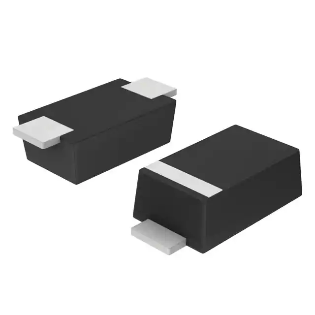
Surface Mount
Schottky Power Rectifier
This device employs the Schottky Barrier principle in a large area
metal−to−silicon power diode. State−of−the−art geometry features
epitaxial construction with oxide passivation and metal overlay
contact. Ideally suited for low voltage, high frequency rectification, or
as free wheeling and polarity protection diodes in surface mount
applications where compact size and weight are critical to the system.
Features
•
•
•
•
•
•
•
www.onsemi.com
SCHOTTKY BARRIER
RECTIFIER
2.0 AMPERE
60 VOLTS
Low Profile Package for Space Constrained Applications
Rectangular Package for Automated Handling
Highly Stable Oxide Passivated Junction
150°C Operating Junction Temperature
Guard−Ring for Stress Protection
NRVB Prefix for Automotive and Other Applications Requiring
Unique Site and Control Change Requirements; AEC−Q101
Qualified and PPAP Capable
These are Pb−Free and Halide−Free Devices
SMA−FL
CASE 403AA
STYLE 6
MARKING DIAGRAM
Mechanical Charactersistics
• Case: Epoxy, Molded, Epoxy Meets UL 94, V−0
• Weight: 95 mg (approximately)
• Finish: All External Surfaces Corrosion Resistant and Terminal
•
•
•
•
Leads are Readily Solderable
Lead and Mounting Surface Temperature for Soldering Purposes:
260°C Max. for 10 Seconds
Cathode Polarity Band
Device Meets MSL 1 Requirements
ESD Ratings: Machine Model = C
ESD Ratings: Human Body Model = 3B
RAG
AYWWG
RAG
A
Y
WW
G
= Specific Device Code
= Assembly Location
= Year
= Work Week
= Pb−Free Package
ORDERING INFORMATION
Device
Package
Shipping†
MBRAF260T3G
SMA−FL
(Pb−Free)
5000 / Tape & Reel
NRVBAF260T3G
SMA−FL
(Pb−Free)
5000 / Tape & Reel
†For information on tape and reel specifications,
including part orientation and tape sizes, please
refer to our Tape and Reel Packaging Specification
Brochure, BRD8011/D.
© Semiconductor Components Industries, LLC, 2016
December, 2016 − Rev. 3
1
Publication Order Number:
MBRAF260/D
�MBRAF260T3G, NRVBAF260T3G
MAXIMUM RATINGS
Rating
Peak Repetitive Reverse Voltage
Working Peak Reverse Voltage
DC Blocking Voltage
Average Rectified Forward Current
(At Rated VR, TL = 120°C)
Symbol
Value
Unit
VRRM
VRWM
VR
60
V
IO
A
2.0
Peak Repetitive Forward Current
(Rated VR, Square Wave, 20 kHz) TL = 90°C
IFRM
A
Non−Repetitive Peak Surge Current
(Surge Applied at Rated Load Conditions Halfwave, Single Phase, 60 Hz)
IFSM
Storage Temperature Range
Tstg
−55 to +150
°C
Operating Junction Temperature
TJ
−55 to +150
°C
4.0
A
60
Voltage Rate of Change
(Rated VR, TJ = 25°C)
dv/dt
V/ms
10,000
Controlled Avalanche Energy (see test conditions in Figures 6 and 7)
WAVAL
10
mJ
Stresses exceeding those listed in the Maximum Ratings table may damage the device. If any of these limits are exceeded, device functionality
should not be assumed, damage may occur and reliability may be affected.
THERMAL CHARACTERISTICS
Characteristic
Thermal Resistance, Junction−to−Lead (Note 1)
Thermal Resistance, Junction−to−Ambient (Note 1)
Symbol
Value
Unit
RqJL
RqJA
25
90
°C/W
1. 1 inch square pad size (1 x 0.5 inch for each lead) on FR4 board.
ELECTRICAL CHARACTERISTICS
Characteristic
Symbol
vF
Maximum Instantaneous Forward Voltage (Note 2)
(iF = 1.0 A)
(iF = 2.0 A)
Maximum Instantaneous Reverse Current (Note 2)
IR
(VR = 60 V)
Value
Unit
TJ = 25°C
TJ = 125°C
0.51
0.63
0.475
0.55
TJ = 25°C
TJ = 125°C
0.2
20
V
mA
Product parametric performance is indicated in the Electrical Characteristics for the listed test conditions, unless otherwise noted. Product
performance may not be indicated by the Electrical Characteristics if operated under different conditions.
2. Pulse Test: Pulse Width ≤ 250 ms, Duty Cycle ≤ 2.0%.
www.onsemi.com
2
�MBRAF260T3G, NRVBAF260T3G
10
IF, INSTANTANEOUS FORWARD
CURRENT (AMPS)
IF, INSTANTANEOUS FORWARD
CURRENT (AMPS)
10
75°C
125°C
25°C
1
0.1
75°C
125°C
25°C
1
0.1
0.1
0.2
0.3
0.4
0.5
0.6
0.7
0.8
0.1
0.2
0.3
0.4
0.5
0.6
0.8
VF, INSTANTANEOUS FORWARD VOLTAGE (VOLTS)
Figure 1. Typical Forward Voltage
Figure 2. Maximum Forward Voltage
1.0E−02
100
IR, REVERSE CURRENT (AMPS)
125°C
25°C
f = 1 MHz
C, CAPACITANCE (pF)
1.0E−03
75°C
1.0E−04
1.0E−05
25°C
1.0E−06
1.0E−07
R(t), TYPICAL TRANSIENT THERMAL
RESISTANCE (°C/W)
0.7
VF, INSTANTANEOUS FORWARD VOLTAGE (VOLTS)
10
0
10
20
30
40
50
60
0
10
20
30
50
40
VR, REVERSE VOLTAGE (VOLTS)
VR, REVERSE VOLTAGE (VOLTS)
Figure 3. Typical Reverse Current
Figure 4. Typical Capacitance
60
100
50% Duty Cycle
10
20%
10%
5%
2%
1
1%
0.1
0.01
Single Pulse
0.001
0.0000001 0.000001
0.00001
0.0001
0.001
0.01
0.1
1
10
t, PULSE TIME (S)
Figure 5. Typical Transient Thermal Response, Junction−to−Ambient
www.onsemi.com
3
100
1000
�MBRAF260T3G, NRVBAF260T3G
+VDD
IL
10 mH COIL
BVDUT
VD
MERCURY
SWITCH
ID
ID
IL
DUT
S1
VDD
t0
Figure 6. Test Circuit
t1
t2
t
Figure 7. Current−Voltage Waveforms
The unclamped inductive switching circuit shown in
Figure 6 was used to demonstrate the controlled avalanche
capability of this device. A mercury switch was used instead
of an electronic switch to simulate a noisy environment
when the switch was being opened.
When S1 is closed at t0 the current in the inductor IL ramps
up linearly; and energy is stored in the coil. At t1 the switch
is opened and the voltage across the diode under test begins
to rise rapidly, due to di/dt effects, when this induced voltage
reaches the breakdown voltage of the diode, it is clamped at
BVDUT and the diode begins to conduct the full load current
which now starts to decay linearly through the diode, and
goes to zero at t2.
By solving the loop equation at the point in time when S1
is opened; and calculating the energy that is transferred to
the diode it can be shown that the total energy transferred is
equal to the energy stored in the inductor plus a finite amount
of energy from the VDD power supply while the diode is in
breakdown (from t1 to t2) minus any losses due to finite
component resistances. Assuming the component resistive
elements are small Equation (1) approximates the total
energy transferred to the diode. It can be seen from this
equation that if the VDD voltage is low compared to the
breakdown voltage of the device, the amount of energy
contributed by the supply during breakdown is small and the
total energy can be assumed to be nearly equal to the energy
stored in the coil during the time when S1 was closed,
Equation (2).
EQUATION (1):
ǒ
BV
2
DUT
W
[ 1 LI LPK
AVAL
2
V
BV
DUT DD
EQUATION (2):
2
W
[ 1 LI LPK
AVAL
2
www.onsemi.com
4
Ǔ
�MECHANICAL CASE OUTLINE
PACKAGE DIMENSIONS
SMA−FL
CASE 403AA−01
ISSUE O
DATE 02 MAR 2011
SCALE 2:1
E
E1
NOTES:
1. DIMENSIONING AND TOLERANCING PER
ASME Y14.5M, 1994.
2. CONTROLLING DIMENSION: MILLIMETERS.
D
DIM
A
b
c
D
E
E1
L
TOP VIEW
A
c
2X
C
SIDE VIEW
MILLIMETERS
MIN
MAX
0.90
1.10
1.25
1.65
0.15
0.30
2.40
2.80
4.80
5.40
4.00
4.60
0.70
1.10
SEATING
PLANE
b
2X
L
BOTTOM VIEW
RECOMMENDED
SOLDER FOOTPRINT*
5.56
1.76
1.30
DIMENSIONS: MILLIMETERS
*For additional information on our Pb−Free strategy and soldering
details, please download the ON Semiconductor Soldering and
Mounting Techniques Reference Manual, SOLDERRM/D.
DOCUMENT NUMBER:
DESCRIPTION:
98AON55210E
SMA−FL
Electronic versions are uncontrolled except when accessed directly from the Document Repository.
Printed versions are uncontrolled except when stamped “CONTROLLED COPY” in red.
PAGE 1 OF 1
ON Semiconductor and
are trademarks of Semiconductor Components Industries, LLC dba ON Semiconductor or its subsidiaries in the United States and/or other countries.
ON Semiconductor reserves the right to make changes without further notice to any products herein. ON Semiconductor makes no warranty, representation or guarantee regarding
the suitability of its products for any particular purpose, nor does ON Semiconductor assume any liability arising out of the application or use of any product or circuit, and specifically
disclaims any and all liability, including without limitation special, consequential or incidental damages. ON Semiconductor does not convey any license under its patent rights nor the
rights of others.
© Semiconductor Components Industries, LLC, 2019
www.onsemi.com
�onsemi,
, and other names, marks, and brands are registered and/or common law trademarks of Semiconductor Components Industries, LLC dba “onsemi” or its affiliates
and/or subsidiaries in the United States and/or other countries. onsemi owns the rights to a number of patents, trademarks, copyrights, trade secrets, and other intellectual property.
A listing of onsemi’s product/patent coverage may be accessed at www.onsemi.com/site/pdf/Patent−Marking.pdf. onsemi reserves the right to make changes at any time to any
products or information herein, without notice. The information herein is provided “as−is” and onsemi makes no warranty, representation or guarantee regarding the accuracy of the
information, product features, availability, functionality, or suitability of its products for any particular purpose, nor does onsemi assume any liability arising out of the application or use
of any product or circuit, and specifically disclaims any and all liability, including without limitation special, consequential or incidental damages. Buyer is responsible for its products
and applications using onsemi products, including compliance with all laws, regulations and safety requirements or standards, regardless of any support or applications information
provided by onsemi. “Typical” parameters which may be provided in onsemi data sheets and/or specifications can and do vary in different applications and actual performance may
vary over time. All operating parameters, including “Typicals” must be validated for each customer application by customer’s technical experts. onsemi does not convey any license
under any of its intellectual property rights nor the rights of others. onsemi products are not designed, intended, or authorized for use as a critical component in life support systems
or any FDA Class 3 medical devices or medical devices with a same or similar classification in a foreign jurisdiction or any devices intended for implantation in the human body. Should
Buyer purchase or use onsemi products for any such unintended or unauthorized application, Buyer shall indemnify and hold onsemi and its officers, employees, subsidiaries, affiliates,
and distributors harmless against all claims, costs, damages, and expenses, and reasonable attorney fees arising out of, directly or indirectly, any claim of personal injury or death
associated with such unintended or unauthorized use, even if such claim alleges that onsemi was negligent regarding the design or manufacture of the part. onsemi is an Equal
Opportunity/Affirmative Action Employer. This literature is subject to all applicable copyright laws and is not for resale in any manner.
PUBLICATION ORDERING INFORMATION
LITERATURE FULFILLMENT:
Email Requests to: orderlit@onsemi.com
onsemi Website: www.onsemi.com
◊
TECHNICAL SUPPORT
North American Technical Support:
Voice Mail: 1 800−282−9855 Toll Free USA/Canada
Phone: 011 421 33 790 2910
Europe, Middle East and Africa Technical Support:
Phone: 00421 33 790 2910
For additional information, please contact your local Sales Representative
�