ON Semiconductor
Is Now
To learn more about onsemi™, please visit our website at
www.onsemi.com
onsemi and and other names, marks, and brands are registered and/or common law trademarks of Semiconductor Components Industries, LLC dba “onsemi” or its affiliates and/or
subsidiaries in the United States and/or other countries. onsemi owns the rights to a number of patents, trademarks, copyrights, trade secrets, and other intellectual property. A listing of onsemi
product/patent coverage may be accessed at www.onsemi.com/site/pdf/Patent-Marking.pdf. onsemi reserves the right to make changes at any time to any products or information herein, without
notice. The information herein is provided “as-is” and onsemi makes no warranty, representation or guarantee regarding the accuracy of the information, product features, availability, functionality,
or suitability of its products for any particular purpose, nor does onsemi assume any liability arising out of the application or use of any product or circuit, and specifically disclaims any and all
liability, including without limitation special, consequential or incidental damages. Buyer is responsible for its products and applications using onsemi products, including compliance with all laws,
regulations and safety requirements or standards, regardless of any support or applications information provided by onsemi. “Typical” parameters which may be provided in onsemi data sheets and/
or specifications can and do vary in different applications and actual performance may vary over time. All operating parameters, including “Typicals” must be validated for each customer application
by customer’s technical experts. onsemi does not convey any license under any of its intellectual property rights nor the rights of others. onsemi products are not designed, intended, or authorized
for use as a critical component in life support systems or any FDA Class 3 medical devices or medical devices with a same or similar classification in a foreign jurisdiction or any devices intended for
implantation in the human body. Should Buyer purchase or use onsemi products for any such unintended or unauthorized application, Buyer shall indemnify and hold onsemi and its officers, employees,
subsidiaries, affiliates, and distributors harmless against all claims, costs, damages, and expenses, and reasonable attorney fees arising out of, directly or indirectly, any claim of personal injury or death
associated with such unintended or unauthorized use, even if such claim alleges that onsemi was negligent regarding the design or manufacture of the part. onsemi is an Equal Opportunity/Affirmative
Action Employer. This literature is subject to all applicable copyright laws and is not for resale in any manner. Other names and brands may be claimed as the property of others.
�Very Low Forward Voltage
Trench-based Schottky
Rectifier
Exceptionally Low VF = 0.53 V at IF = 5 A
NTSB40200CT,
NRVTSB40200CT,
NTSJ40200CT
www.onsemi.com
VERY LOW FORWARD
VOLTAGE, LOW LEAKAGE
SCHOTTKY BARRIER
RECTIFIERS 40 AMPERES,
200 VOLTS
Features
• Fine Lithography Trench−based Schottky Technology for Very Low
•
•
•
•
•
•
•
Forward Voltage and Low Leakage
Fast Switching with Exceptional Temperature Stability
Low Power Loss and Lower Operating Temperature
Higher Efficiency for Achieving Regulatory Compliance
Low Thermal Resistance
High Surge Capability
NRV Prefix for Automotive and Other Applications Requiring
Unique Site and Control Change Requirements; AEC−Q101
Qualified and PPAP Capable
These Devices are Pb−Free and Halogen Free/BFR Free
PIN CONNECTIONS
1
2, 4
3
4
Typical Applications
• Switching Power Supplies including Telecom AC to DC Power
•
•
•
•
Stages, LED Lighting and ATX
High Voltage DC−DC Converters
Freewheeling and OR−ing Diodes
Output Rectifier in Welding Power Supplies
Industrial Automation
1
Mechanical Characteristics
• Case: Epoxy, Molded
• Epoxy Meets Flammability Rating UL 94−0 @ 0.125 in
• Finish: All External Surfaces Corrosion Resistant and Terminal
2
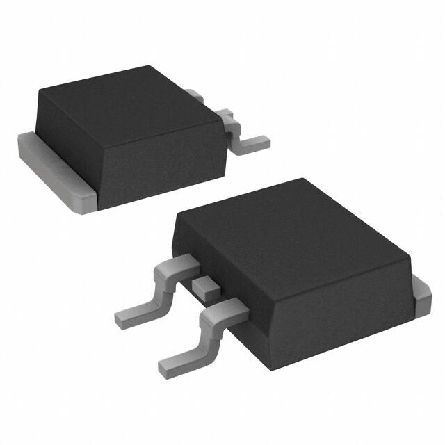
TO−220FP
CASE 221AH
D2PAK−3
CASE 418B
3
ORDERING INFORMATION
See detailed ordering and shipping information in the package
dimensions section on page 6 of this data sheet.
Leads are Readily Solderable
• Lead Temperature for Soldering Purposes:
260°C Maximum for 10 s
This document contains information on some products that are still under development.
ON Semiconductor reserves the right to change or discontinue these products without
notice.
© Semiconductor Components Industries, LLC, 2014
August, 2020 − Rev. 2
1
Publication Order Number:
NTSB40200CT/D
�NTSB40200CT, NRVTSB40200CT, NTSJ40200CT
MAXIMUM RATINGS
Symbol
Value
Unit
Peak Repetitive Reverse Voltage
Working Peak Reverse Voltage
DC Blocking Voltage
Rating
VRRM
VRWM
VR
200
V
Average Rectified Forward Current
(Rated VR, TC = 125°C) NTSB40200CT, NRVTSB40200CT Per device
(Rated VR, TC = 130°C) NTSB40200CT, NRVTSB40200CT Per diode
IF(AV)
A
40
20
20
20
(Rated VR, TC = 65°C) NTSJ40200CT Per device
(Rated VR, TC = 42°C) NTSJ40200CT Per diode
Peak Repetitive Forward Current
(Rated VR, Square Wave, 20 kHz, TC = 115°C) NTSB40200CT, NRVTSB40200CT Per device
(Rated VR, Square Wave, 20 kHz, TC = 125°C) NTSB40200CT, NRVTSB40200CT Per diode
IFRM
A
80
40
(Rated VR, Square Wave, 20 kHz, TC = 40°C) NTSJ40200CT Per device
(Rated VR, Square Wave, 20 kHz, TC = 25°C) NTSJ40200CT Per diode
40
40
Nonrepetitive Peak Surge Current
(Surge applied at rated load conditions halfwave, single phase, 60 Hz)
IFSM
250
A
Operating Junction Temperature
TJ
−55 to +150
°C
Storage Temperature
Tstg
−55 to +150
°C
ESD Rating (Human Body Model)
3A
ESD Rating (Machine Model)
M4
Stresses exceeding those listed in the Maximum Ratings table may damage the device. If any of these limits are exceeded, device functionality
should not be assumed, damage may occur and reliability may be affected.
THERMAL CHARACTERISTICS
Rating
Typical Thermal Resistance
Symbol
NTSB40200CT
NRVTSB40200CT
NTSJ40200CT
Junction−to−Case Per Diode
Junction−to−Case Per Device
RqJC
1.29
0.79
6.94
6.05
Junction−to−Ambient Per Device
RqJA
40
105
Unit
°C/W
ELECTRICAL CHARACTERISTICS
Rating
Symbol
Instantaneous Forward Voltage (Note 1)
(IF = 5 A, TJ = 25°C)
(IF = 10 A, TJ = 25°C)
(IF = 15 A, TJ = 25°C)
(IF = 20 A, TJ = 25°C)
VF
(IF = 5 A, TJ = 125°C)
(IF = 10 A, TJ = 125°C)
(IF = 15 A, TJ = 125°C)
(IF = 20 A, TJ = 125°C)
Instantaneous Reverse Current (Note 1)
(VR = 180 V, TJ = 25°C)
(Rated dc Voltage, TJ = 25°C)
IR
(VR = 180 V, TJ = 125°C)
(Rated dc Voltage, TJ = 125°C)
Typ
Max
0.68
0.74
0.79
0.84
−
−
−
1.45
0.53
0.60
0.64
0.68
−
−
−
0.80
3
5
−
100
mA
mA
5.3
7
−
30
mA
mA
Unit
V
Product parametric performance is indicated in the Electrical Characteristics for the listed test conditions, unless otherwise noted. Product
performance may not be indicated by the Electrical Characteristics if operated under different conditions.
1. Pulse Test: Pulse Width = 300 ms, Duty Cycle v 2.0%
www.onsemi.com
2
�NTSB40200CT, NRVTSB40200CT, NTSJ40200CT
TYPICAL CHARACTERISTICS
100
TA = 125°C
TA = 150°C
1
0.1
TA = 25°C
TA = −55°C
0.0
0.2
0.4
0.6
0.8
1.0
1.2
TA = 125°C
10
TA = 150°C
TA = 25°C
1
TA = −55°C
0.1
0.00
1.4
0.80
1.20
1.60
2.00
2.40
VF, INSTANTANEOUS FORWARD VOLTAGE (V)
Figure 1. Typical Instantaneous Forward
Characteristics
Figure 2. Maximum Instantaneous Forward
Characteristics
1.E−01
1.E−02
TA = 150°C
1.E−03
TA = 125°C
TA = 150°C
1.E−02
TA = 125°C
1.E−03
1.E−04
1.E−04
1.E−05
TA = 25°C
1.E−06
TA = 25°C
1.E−05
1.E−07
0
20
40
60
TA = −55°C
1.E−06
TA = −55°C
1.E−08
1.E−09
0.40
VF, INSTANTANEOUS FORWARD VOLTAGE (V)
80
100 120 140 160 180 200
VR, INSTANTANEOUS REVERSE VOLTAGE (V)
1.E−07
0
Figure 3. Typical Reverse Characteristics
20
40
1k
100
1
80
100 120 140 160 180 200
Figure 4. Maximum Reverse Characteristics
TJ = 25°C
10
60
VR, INSTANTANEOUS REVERSE VOLTAGE (V)
10k
C, JUNCTION CAPACITANCE (pF)
IR, INSTANTANEOUS REVERSE CURRENT (A)
iF, INSTANTANEOUS FORWARD
CURRENT (A)
10
IR, INSTANTANEOUS REVERSE CURRENT (A)
iF, INSTANTANEOUS FORWARD
CURRENT (A)
100
10
100
VR, REVERSE VOLTAGE (V)
Figure 5. Typical Junction Capacitance
www.onsemi.com
3
�NTSB40200CT, NRVTSB40200CT, NTSJ40200CT
TYPICAL CHARACTERISTICS
35
DC
30
25
Square Wave
20
15
10
5
0
0
20
40
60
80
120
30
20
10
0
20
40
60
80
80
IF(AV), AVERAGE FORWARD
CURRENT (A)
30
DC
20
Square Wave
10
5
0
40
100
120
Figure 7. Current Derating per Device
(NTSB40200CT & NRVTSB40200CT)
35
15
Square Wave
Figure 6. Current Derating per Diode
(NTSB40200CT & NRVTSB40200CT)
RqJC = 6.94°C/W
25
50
0
140
DC
60
TC, CASE TEMPERATURE (°C)
20
40
60
80
100
120
60
50
40
DC
30
20
Square Wave
10
0
140
0
20
40
60
80
100
120
TC, CASE TEMPERATURE (°C)
Figure 8. Current Derating per Diode
(NTSJ40200CT)
Figure 9. Current Derating per Device
(NTSJ40200CT)
60
55
IPK/IAV = 10
50
45
IPK/IAV = 5
IPK/IAV = 20
40
Square Wave
35
30
dc
25
20
15
10
5
0
TJ = 150°C
0
5
10
15
20
25
30
35
IF(AV), AVERAGE FORWARD CURRENT (A)
Figure 10. Forward Power Dissipation
www.onsemi.com
4
140
RqJC = 6.05°C/W
70
TC, CASE TEMPERATURE (°C)
PF(AV), AVERAGE FORWARD
POWER DISSIPATION (W)
IF(AV), AVERAGE FORWARD
CURRENT (A)
100
RqJC = 0.79°C/W
70
TC, CASE TEMPERATURE (°C)
40
0
80
RqJC = 1.29°C/W
IF(AV), AVERAGE FORWARD
CURRENT (A)
IF(AV), AVERAGE FORWARD
CURRENT (A)
40
40
140
�NTSB40200CT, NRVTSB40200CT, NTSJ40200CT
TYPICAL CHARACTERISTICS
R(t), TYPICAL TRANSIENT THERMAL
RESISTANCE (°C/W)
100
50%
10 20%
10%
5%
1 2%
RqJA = 40°C/W
1%
0.1
0.01
0.001
Single Pulse
Psi Tab−A
0.000001
0.00001
0.0001
0.001
0.01
0.1
1
10
100
1000
t, PULSE TIME (sec)
R(t), TYPICAL TRANSIENT THERMAL
RESISTANCE (°C/W)
Figure 11. Typical Transient Thermal Response per Device (NTSB40200CTG)
10
50%
RqJC = 6.05°C/W
20%
1 10%
5%
0.1
0.01
0.001
2%
1%
Single Pulse
0.000001
0.00001
0.0001
0.001
0.01
0.1
1
10
t, PULSE TIME (sec)
Figure 12. Typical Transient Thermal Response per Device (NTSJ40200CTG)
www.onsemi.com
5
100
1000
�NTSB40200CT, NRVTSB40200CT, NTSJ40200CT
ORDERING INFORMATION
Package
Shipping
NTSB40200CTG
Device
D2PAK−3
(Pb−Free)
50 Units / Rail
NTSB40200CTT4G
D2PAK−3
(Pb−Free)
800 / Tape & Reel
NRVTSB40200CTT4G*
D2PAK−3
(Pb−Free)
800 / Tape & Reel
TO−220FP
(Halide−Free)
50 Units / Rail
NTSJ40200CTG
(In Development)
*NRV Prefix for Automotive and Other Applications Requiring Unique Site and Control Change Requirements; AEC−Q101 Qualified and PPAP
Capable.
MARKING DIAGRAMS
AY WW
TS40200CG
AKA
AYWW
TS40200CG
AKA
D2PAK−3
A
Y
WW
AKA
G
TO−220FP
= Assembly Location
= Year
= Work Week
= Polarity Designator
= Pb−Free Package
www.onsemi.com
6
�NTSB40200CT, NRVTSB40200CT, NTSJ40200CT
PACKAGE DIMENSIONS
TO−220 FULLPACK, 3−LEAD
CASE 221AH
ISSUE D
A
E
B
P
E/2
0.14
Q
D
M
B A
M
A
H1
A1
C
NOTE 3
1 2 3
L
L1
3X
3X
b2
SEATING
PLANE
c
b
0.25
M
B A
M
C
A2
e
www.onsemi.com
7
NOTES:
1. DIMENSIONING AND TOLERANCING PER ASME
Y14.5M, 1994.
2. CONTROLLING DIMENSION: MILLIMETERS.
3. CONTOUR UNCONTROLLED IN THIS AREA.
4. DIMENSIONS D AND E DO NOT INCLUDE MOLD FLASH
AND GATE PROTRUSIONS. MOLD FLASH AND GATE
PROTRUSIONS NOT TO EXCEED 0.13 PER SIDE. THESE
DIMENSIONS ARE TO BE MEASURED AT OUTERMOST
EXTREME OF THE PLASTIC BODY.
5. DIMENSION b2 DOES NOT INCLUDE DAMBAR
PROTRUSION. LEAD WIDTH INCLUDING PROTRUSION
SHALL NOT EXCEED 2.00.
DIM
A
A1
A2
b
b2
c
D
E
e
H1
L
L1
P
Q
MILLIMETERS
MIN
MAX
4.30
4.70
2.50
2.90
2.50
2.70
0.54
0.84
1.10
1.40
0.49
0.79
14.70
15.30
9.70
10.30
2.54 BSC
6.70
7.10
12.70
14.73
--2.10
3.00
3.40
2.80
3.20
�NTSB40200CT, NRVTSB40200CT, NTSJ40200CT
PACKAGE DIMENSIONS
D2PAK 3
CASE 418B−04
ISSUE L
NOTES:
1. DIMENSIONING AND TOLERANCING
PER ANSI Y14.5M, 1982.
2. CONTROLLING DIMENSION: INCH.
3. 418B−01 THRU 418B−03 OBSOLETE,
NEW STANDARD 418B−04.
C
E
−B−
V
W
4
1
2
A
S
3
−T−
SEATING
PLANE
DIM
A
B
C
D
E
F
G
H
J
K
L
M
N
P
R
S
V
K
J
G
D 3 PL
0.13 (0.005)
W
H
M
T B
M
VARIABLE
CONFIGURATION
ZONE
N
R
MILLIMETERS
MIN
MAX
8.64
9.65
9.65 10.29
4.06
4.83
0.51
0.89
1.14
1.40
7.87
8.89
2.54 BSC
2.03
2.79
0.46
0.64
2.29
2.79
1.32
1.83
7.11
8.13
5.00 REF
2.00 REF
0.99 REF
14.60 15.88
1.14
1.40
P
U
L
M
INCHES
MIN
MAX
0.340 0.380
0.380 0.405
0.160 0.190
0.020 0.035
0.045 0.055
0.310 0.350
0.100 BSC
0.080
0.110
0.018 0.025
0.090
0.110
0.052 0.072
0.280 0.320
0.197 REF
0.079 REF
0.039 REF
0.575 0.625
0.045 0.055
L
M
L
M
F
F
F
VIEW W−W
1
VIEW W−W
2
VIEW W−W
3
ON Semiconductor and
are trademarks of Semiconductor Components Industries, LLC dba ON Semiconductor or its subsidiaries in the United States and/or other countries.
ON Semiconductor owns the rights to a number of patents, trademarks, copyrights, trade secrets, and other intellectual property. A listing of ON Semiconductor’s product/patent
coverage may be accessed at www.onsemi.com/site/pdf/Patent−Marking.pdf. ON Semiconductor reserves the right to make changes without further notice to any products herein.
ON Semiconductor makes no warranty, representation or guarantee regarding the suitability of its products for any particular purpose, nor does ON Semiconductor assume any liability
arising out of the application or use of any product or circuit, and specifically disclaims any and all liability, including without limitation special, consequential or incidental damages.
Buyer is responsible for its products and applications using ON Semiconductor products, including compliance with all laws, regulations and safety requirements or standards,
regardless of any support or applications information provided by ON Semiconductor. “Typical” parameters which may be provided in ON Semiconductor data sheets and/or
specifications can and do vary in different applications and actual performance may vary over time. All operating parameters, including “Typicals” must be validated for each customer
application by customer’s technical experts. ON Semiconductor does not convey any license under its patent rights nor the rights of others. ON Semiconductor products are not
designed, intended, or authorized for use as a critical component in life support systems or any FDA Class 3 medical devices or medical devices with a same or similar classification
in a foreign jurisdiction or any devices intended for implantation in the human body. Should Buyer purchase or use ON Semiconductor products for any such unintended or unauthorized
application, Buyer shall indemnify and hold ON Semiconductor and its officers, employees, subsidiaries, affiliates, and distributors harmless against all claims, costs, damages, and
expenses, and reasonable attorney fees arising out of, directly or indirectly, any claim of personal injury or death associated with such unintended or unauthorized use, even if such
claim alleges that ON Semiconductor was negligent regarding the design or manufacture of the part. ON Semiconductor is an Equal Opportunity/Affirmative Action Employer. This
literature is subject to all applicable copyright laws and is not for resale in any manner.
PUBLICATION ORDERING INFORMATION
LITERATURE FULFILLMENT:
Email Requests to: orderlit@onsemi.com
ON Semiconductor Website: www.onsemi.com
◊
TECHNICAL SUPPORT
North American Technical Support:
Voice Mail: 1 800−282−9855 Toll Free USA/Canada
Phone: 011 421 33 790 2910
www.onsemi.com
8
Europe, Middle East and Africa Technical Support:
Phone: 00421 33 790 2910
For additional information, please contact your local Sales Representative
�