NSBC114EPDP6T5G Series
Preferred Devices
Dual Digital Transistors (BRT)
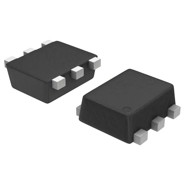
Complementary Silicon Surface Mount Transistors with Monolithic Bias Resistor Network
The BRT (Bias Resistor Transistor) contains a single transistor with a monolithic bias network consisting of two resistors; a series base resistor and a base−emitter resistor. These digital transistors are designed to replace a single device and its external resistor bias network. The BRT eliminates these individual components by integrating them into a single device. In the NSBC114EPDP6T5G series, two complementary BRT devices are housed in the SOT−963 package which is ideal for low power surface mount applications where board space is at a premium.
Features
(3) R1 Q1 R2 (4)
http://onsemi.com
(2) R2 Q2 R1 (5) (6) (1)
• • • • • •
Simplifies Circuit Design Reduces Board Space Reduces Component Count Available in 4 mm, 8000 Units Tape and Reel These are Pb−Free Devices These are Halide−Free Devices
MARKING DIAGRAM
XM 1
SOT−963 CASE 527AD
MAXIMUM RATINGS (TA = 25°C unless otherwise noted, common for Q1
and Q2, − minus sign for Q1 (PNP) omitted) Rating Collector-Base Voltage Collector-Emitter Voltage Collector Current Symbol VCBO VCEO IC Value 50 50 100 Unit Vdc Vdc mAdc
X M G
= Specific Device Code = Date Code = Pb−Free Package
ORDERING INFORMATION
Device Package Shipping† 8000 / Tape & Reel
Stresses exceeding Maximum Ratings may damage the device. Maximum Ratings are stress ratings only. Functional operation above the Recommended Operating Conditions is not implied. Extended exposure to stresses above the Recommended Operating Conditions may affect device reliability.
NSBC114EPDP6T5G SOT−963 (Pb−Free)
†For information on tape and reel specifications, including part orientation and tape sizes, please refer to our Tape and Reel Packaging Specifications Brochure, BRD8011/D.
DEVICE MARKING INFORMATION
See specific marking information in the device marking table on page 2 of this data sheet.
© Semiconductor Components Industries, LLC, 2008
July, 2008 − Rev. 1
1
Publication Order Number: NSBC114EPDP6/D
�NSBC114EPDP6T5G Series
THERMAL CHARACTERISTICS
Characteristic SINGLE HEATED Total Device Dissipation TA = 25°C (Note 1) Derate above 25°C Thermal Resistance (Note 1) Junction-to-Ambient Total Device Dissipation TA = 25°C (Note 2) Derate above 25°C Thermal Resistance (Note 2) Junction-to-Ambient DUAL HEATED (Note 3) Total Device Dissipation TA = 25°C (Note 1) Derate above 25°C Thermal Resistance (Note 1) Junction-to-Ambient Total Device Dissipation TA = 25°C (Note 2) Derate above 25°C Thermal Resistance (Note 2) Junction-to-Ambient Junction and Storage Temperature PD 339 2.7 369 mW mW/°C °C/W PD 231 1.9 540 mW mW/°C °C/W Symbol Max Unit
RqJA PD
269 2.2 464
mW mW/°C °C/W
RqJA
RqJA PD
408 3.3 306 − 55 to +150
mW mW/°C °C/W °C
RqJA TJ, Tstg
1. FR−4 @ 100 mm2, 1 oz. copper traces, still air. 2. FR−4 @ 500 mm2, 1 oz. copper traces, still air. 3. Dual heated values assume total power is sum of two equally powered channels.
DEVICE MARKING AND RESISTOR VALUES
Device NSBC114EPDP6T5G NSBC124EPDP6T5G NSBC144EPDP6T5G NSBC114YPDP6T5G NSBC115TPDP6T5G NSBC123TPDP6T5G NSBC143EPDP6T5G NSBC143ZPDP6T5G NSBC144WPDP6T5G NSBC123JPDP6T5G Package SOT−963 SOT−963 SOT−963 SOT−963 SOT−963 SOT−963 SOT−963 SOT−963 SOT−963 SOT−963 Marking (Clockwise Rotation) L R (90°) K (180°) Q (90°) J (180°) A (180°) V (90°) Y (90°) T (90°) D (180°) R1 (kW) 10 22 47 10 100 2.2 4.7 4.7 47 2.2 R2 (kW) 10 22 47 47 ∞ ∞ 4.7 47 22 47
http://onsemi.com
2
�NSBC114EPDP6T5G Series
ELECTRICAL CHARACTERISTICS
(TA = 25°C unless otherwise noted, common for Q1 and Q2, − minus sign for Q1 (PNP) omitted) TCharacteristic OFF CHARACTERISTICS Collector-Base Cutoff Current (VCB = 50 V, IE = 0) Collector-Emitter Cutoff Current (VCE = 50 V, IB = 0) Emitter-Base Cutoff Current (VEB = 6.0 V, IC = 0) NSBC114EPDP6T5G NSBC124EPDP6T5G NSBC144EPDP5T5G NSBC114YPDP6T5G NSBC115TPDP6T5G NSBC123TPDP6T5G NSBC143EPDP6T5G NSBC143ZPDP6T5G NSBC144WPDP6T5G NSBC123JPDP6T5G ICBO ICEO IEBO − − − − − − − − − − − − 50 50 − − − − − − − − − − − − − − 100 500 0.5 0.2 0.1 0.2 0.1 4.0 1.5 0.18 0.13 0.2 − − nAdc nAdc mAdc Symbol Min Typ Max Unit
Collector-Base Breakdown Voltage (IC = 10 mA, IE = 0) Collector-Emitter Breakdown Voltage (Note 4) (IC = 2.0 mA, IB = 0) ON CHARACTERISTICS (Note 4) DC Current Gain (VCE = 10 V, IC = 5.0 mA) NSBC114EPDP6T5G NSBC124EPDP6T5G NSBC144EPDP5T5G NSBC114YPDP6T5G NSBC115TPDP6T5G NSBC123TPDP6T5G NSBC143EPDP6T5G NSBC143ZPDP6T5G NSBC144WPDP6T5G NSBC123JPDP6T5G
V(BR)CBO V(BR)CEO hFE
Vdc Vdc
35 60 80 80 160 160 15 80 80 80
60 100 140 140 350 350 30 200 140 140
− − − − − − − − − − Vdc
Collector-Emitter Saturation Voltage (IC = 10 mA, IB = 0.3 mA)
VCE(sat) NSBC114EPDP6T5G NSBC124EPDP6T5G NSBC144EPDP6T5G NSBC114YPDP6T5G NSBC144WPDP6T5G NSBC123JPDP6T5G NSBC115TPDP6T5G NSBC143EPDP6T5G NSBC143ZPDP6T5G NSBC123TPDP6T5G VOL − − − − − − VOH 4.9 4.9 4.9 4.9 4.9 4.9 − − − − − − − − − − − − − − − − − − 0.2 0.2 0.2 0.2 0.2 0.2 − − − − − − − − − − − − − − − − − − − − 0.25 0.25 0.25 0.25 0.25 0.25 0.25 0.25 0.25 0.25
(IC = 10 mA, IB = 1 mA)
Output Voltage (on) (VCC = 5.0 V, VB = 2.5 V, RL = 1.0 kW) NSBC114EPDP6T5G/NSBC124EPDP6T5G NSBC114YPDP6T5G/NSBC123TPDP6T5G NSBC143EPDP6T5G/NSBC143ZPDP6T5G NSBC123JPDP6T5G (VCC = 5.0 V, VB = 4.0 V, RL = 1.0 kW) NSBC144WPDP6T5G (VCC = 5.0 V, VB = 3.5 V, RL = 1.0 kW) NSBC144EPDP6T5G/NSBC115TPDP6T5G Output Voltage (off) (VCC = 5.0 V, VB = 0.5 V, RL = 1.0 kW) NSBC114EPDP6T5G/NSBC124EPDP6T5G NSBC144EPDP6T5G/NSBC114YPDP6T5 NSBC143ZPDP6T5G/NSBC144WPDP6T5G NSBC123JPDP6T5G (VCC = 5.0 V, VB = 0.25 V, RL = 1.0 kW) NSBC123TPDP6T5G/NSBC115TPDP6T5G NSBC143EPDP6T5G 4. Pulse Test: Pulse Width < 300 ms, Duty Cycle < 2.0%
Vdc
Vdc
http://onsemi.com
3
�NSBC114EPDP6T5G Series
ELECTRICAL CHARACTERISTICS
(TA = 25°C unless otherwise noted, common for Q1 and Q2, − minus sign for Q1 (PNP) omitted) TCharacteristic ON CHARACTERISTICS (Note 4) Input Resistor NSBC114EPDP6T5G NSBC124EPDP6T5G NSBC144EPDP5T5G NSBC114YPDP6T5G NSBC115TPDP6T5G NSBC123TPDP6T5G NSBC143EPDP6T5G NSBC143ZPDP6T5G NSBC144WPDP6T5G NSBC123JPDP6T5G NSBC114EPDP6T5G NSBC124EPDP6T5G NSBC144EPDP5T5G NSBC114YPDP6T5G NSBC115TPDP6T5G NSBC123TPDP6T5G NSBC143EPDP6T5G NSBC143ZPDP6T5G NSBC144WPDP6T5G NSBC123JPDP6T5G R1 7.0 15.4 32.9 7.0 70 1.54 3.3 3.3 15.4 1.54 0.8 0.8 0.8 0.17 − − 0.8 0.055 1.7 0.038 10 22 47 10 100 2.2 4.7 4.7 47 2.2 1.0 1.0 1.0 0.21 − − 1.0 0.1 2.1 0.047 13 28.6 61.1 13 130 2.86 6.1 6.1 28.6 2.86 1.2 1.2 1.2 0.25 − − 1.2 0.185 2.6 0.056 kW Symbol Min Typ Max Unit
Resistor Ratio
R1/R2
4. Pulse Test: Pulse Width < 300 ms, Duty Cycle < 2.0%
http://onsemi.com
4
�NSBC114EPDP6T5G Series
TYPICAL ELECTRICAL CHARACTERISTICS − NSBC114EPDP6 NPN TRANSISTOR
VCE(SAT), COLLECTOR−TO−EMITTER SATURATION VOLTAGE (V)
1.0 IC/IB = 10
1000 VCE = 10 V hFE, DC CURRENT GAIN 25°C 100 150°C −55°C
TA = 25°C 0.10
TA = 150°C
TA = −55°C
10
0.01
0
5
10 15 20 25 30 35 40 IC, COLLECTOR CURRENT (mA)
45
50
1.0 0.1
Figure 1. VCE(sat) vs. IC
1 10 IC, COLLECTOR CURRENT (mA)
100
Figure 2. DC Current Gain
2.40 COBO, OUTPUT CAPACITANCE (pF) IC, COLLECTOR CURRENT (mA) 2.20 2.00 1.80 1.60 1.40 1.20 1.00 0.80 0 5 10 15 20 25 30 35 40 VCB, COLLECTOR BASE VOLTAGE (V) 45 50
100 150°C
10
1 −55°C 0.1 25°C
0.01 0.5
1
1.5
Figure 3. Output Capacitance
Figure 4. Output Current vs. Input Voltage
2 2.5 3 3.5 Vin, INPUT VOLTAGE (V)
4
4.5
5
10
Vin, INPUT VOLTAGE (V)
−55°C 25°C 1.0 150°C
0.10
0
5
10
15
20
25
30
35
40
45
50
Figure 5. Input Voltage vs. Output Current
IC, COLLECTOR CURRENT (mA)
http://onsemi.com
5
�NSBC114EPDP6T5G Series
TYPICAL ELECTRICAL CHARACTERISTICS − NSBC114EPDP6 PNP TRANSISTOR
VCE(SAT), COLLECTOR−TO−EMITTER SATURATION VOLTAGE (V)
1.0 IC/IB = 10 TA = 25°C TA = 150°C 0.10 TA = −55°C
1000 VCE = 10 V hFE, DC CURRENT GAIN
100 150°C 25°C 10 −55°C
0.01
0
5
10 15 20 25 30 35 40 IC, COLLECTOR CURRENT (mA)
45
50
1.0 0.1
Figure 6. VCE(sat) vs. IC
1 10 IC, COLLECTOR CURRENT (mA)
100
Figure 7. DC Current Gain
2.4 COBO, OUTPUT CAPACITANCE (pF) IC, COLLECTOR CURRENT (mA) 2.2 2.0 1.8 1.6 1.4 1.2 1.0 0.8 0 5 10 15 20 25 30 35 40 45 50
100
10
150°C
1.0 −55°C 0.1 25°C
0.01 0
1
2
3
4
5
REVERSE BIAS VOLTAGE (V)
Figure 8. Output Capacitance
10 25°C −55°C 1.0 150°C
Figure 9. Output Current vs. Input Voltage
Vin, INPUT VOLTAGE (V)
Vin, INPUT VOLTAGE (V)
0.1
0
5
10
15
20
25
30
35
40
45
50
Figure 10. Input Voltage vs. Output Current
IC, COLLECTOR CURRENT (mA)
http://onsemi.com
6
�NSBC114EPDP6T5G Series
PACKAGE DIMENSIONS
SOT−963 CASE 527AD−01 ISSUE C
NOTES: 1. DIMENSIONING AND TOLERANCING PER ANSI Y14.5M, 1982. 2. CONTROLLING DIMENSION: MILLIMETERS 3. MAXIMUM LEAD THICKNESS INCLUDES LEAD FINISH THICKNESS. MINIMUM LEAD THICKNESS IS THE MINIMUM THICKNESS OF BASE MATERIAL. DIM A b C D E e L HE MILLIMETERS MIN NOM MAX 0.34 0.37 0.40 0.10 0.15 0.20 0.07 0.12 0.17 0.95 1.00 1.05 0.75 0.80 0.85 0.35 BSC 0.05 0.10 0.15 0.95 1.00 1.05 MIN 0.004 0.003 0.037 0.03 INCHES NOM MAX
D
A B 4 E 3 C 0.08 C A B
A
C L
6
5 12 e
HE
6X
b
0.006 0.008 0.005 0.007 0.039 0.041 0.032 0.034 0.014 BSC 0.002 0.004 0.006 0.037 0.039 0.041
SOLDERING FOOTPRINT*
0.35 0.014 0.35 0.014
0.90 0.0354
0.20 0.08
0.20 0.08
SCALE 20:1
mm inches
*For additional information on our Pb−Free strategy and soldering details, please download the ON Semiconductor Soldering and Mounting Techniques Reference Manual, SOLDERRM/D.
ON Semiconductor and are registered trademarks of Semiconductor Components Industries, LLC (SCILLC). SCILLC reserves the right to make changes without further notice to any products herein. SCILLC makes no warranty, representation or guarantee regarding the suitability of its products for any particular purpose, nor does SCILLC assume any liability arising out of the application or use of any product or circuit, and specifically disclaims any and all liability, including without limitation special, consequential or incidental damages. “Typical” parameters which may be provided in SCILLC data sheets and/or specifications can and do vary in different applications and actual performance may vary over time. All operating parameters, including “Typicals” must be validated for each customer application by customer’s technical experts. SCILLC does not convey any license under its patent rights nor the rights of others. SCILLC products are not designed, intended, or authorized for use as components in systems intended for surgical implant into the body, or other applications intended to support or sustain life, or for any other application in which the failure of the SCILLC product could create a situation where personal injury or death may occur. Should Buyer purchase or use SCILLC products for any such unintended or unauthorized application, Buyer shall indemnify and hold SCILLC and its officers, employees, subsidiaries, affiliates, and distributors harmless against all claims, costs, damages, and expenses, and reasonable attorney fees arising out of, directly or indirectly, any claim of personal injury or death associated with such unintended or unauthorized use, even if such claim alleges that SCILLC was negligent regarding the design or manufacture of the part. SCILLC is an Equal Opportunity/Affirmative Action Employer. This literature is subject to all applicable copyright laws and is not for resale in any manner.
PUBLICATION ORDERING INFORMATION
LITERATURE FULFILLMENT: Literature Distribution Center for ON Semiconductor P.O. Box 5163, Denver, Colorado 80217 USA Phone : 303−675−2175 or 800−344−3860 Toll Free USA/Canada Fax: 303−675−2176 or 800−344−3867 Toll Free USA/Canada Email: orderlit@onsemi.com N. American Technical Support: 800−282−9855 Toll Free USA/Canada Europe, Middle East and Africa Technical Support: Phone: 421 33 790 2910 Japan Customer Focus Center Phone: 81−3−5773−3850 ON Semiconductor Website: www.onsemi.com Order Literature: http://www.onsemi.com/orderlit For additional information, please contact your local Sales Representative
http://onsemi.com
7
NSBC114EPDP6/D
�