NSR0340V2
Schottky Barrier Diode
Schottky barrier diodes are optimized for very low forward voltage
drop and low leakage current and are used in a wide range of dc−dc
converter, clamping and protection applications in portable devices.
NSR0340V2 in a SOD−523 miniature package enables designers to
meet the challenging task of achieving higher efficiency and meeting
reduced space requirements.
Features
•
•
•
•
•
•
•
http://onsemi.com
40 VOLT SCHOTTKY
BARRIER DIODE
Very Low Forward Voltage Drop − 410 mV @ 100 mA
Low Reverse Current − 0.5 mA @ 25 V VR
250 mA of Continuous Forward Current
Power Dissipation of 200 mW with Minimum Trace
Very High Switching Speed
Low Capacitance − CT = 6 pF
This is a Pb−Free Device
1
CATHODE
2
ANODE
2
Typical Applications
•
•
•
•
•
LCD and Keypad Backlighting
Camera Photo Flash
Buck and Boost dc−dc Converters
Reverse Voltage and Current Protection
Clamping & Protection
1
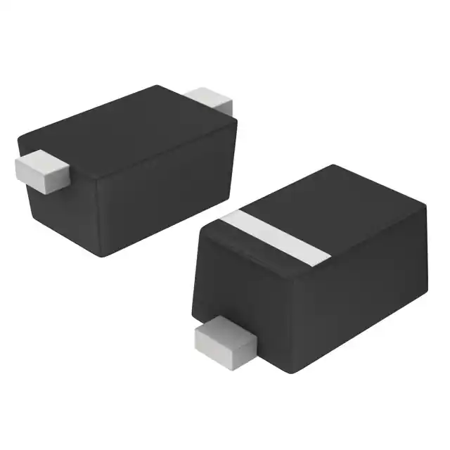
SOD−523
CASE 502
MARKING DIAGRAM
Markets
•
•
•
•
•
Mobile Handsets
MP3 Players
Digital Camera and Camcorders
Notebook PCs and PDAs
GPS
1
Symbol
Value
Unit
Reverse Voltage
VR
40
Vdc
Forward Continuous Current (DC)
IF
250
mA
IFSM
1.0
A
Non−Repetitive Peak Forward Surge
Current
ESD Rating: Human Body Model
Machine Model
ESD
Class 2
Class A
Stresses exceeding Maximum Ratings may damage the device. Maximum
Ratings are stress ratings only. Functional operation above the Recommended
Operating Conditions is not implied. Extended exposure to stresses above the
Recommended Operating Conditions may affect device reliability.
© Semiconductor Components Industries, LLC, 2013
June, 2013 − Rev. 1
2
AD = Device Code
M = Date Code*
G = Pb−Free Package
(Note: Microdot may be in either location)
MAXIMUM RATINGS
Rating
AD M G
G
1
*Date Code orientation position may vary depending
upon manufacturing location.
ORDERING INFORMATION
Device
Package
Shipping†
NSR0340V2T1G SOD−523
(Pb−Free)
3000 / Tape & Reel
NSR0340V2T5G SOD−523
(Pb−Free)
8000 / Tape & Reel
†For information on tape and reel specifications,
including part orientation and tape sizes, please
refer to our Tape and Reel Packaging Specifications
Brochure, BRD8011/D.
Publication Order Number:
NSR0340V2T1/D
�NSR0340V2
THERMAL CHARACTERISTICS
Characteristic
Symbol
Max
Unit
Thermal Resistance
Junction−to−Ambient (Note 1)
Total Power Dissipation @ TA = 25°C
RqJA
PD
600
200
°C/W
mW
Thermal Resistance
Junction−to−Ambient (Note 2)
Total Power Dissipation @ TA = 25°C
RqJA
PD
300
400
°C/W
mW
TJ, Tstg
−55 to +150
°C
Junction and Storage Temperature Range
1. Mounted onto a 4 in square FR−4 board 10 mm sq. 1 oz. Cu 0.06” thick single−sided. Operating to steady state.
2. Mounted onto a 4 in square FR−4 board 1 in sq. 1 oz. Cu 0.06” thick single−sided. Operating to steady state.
ELECTRICAL CHARACTERISTICS (TA = 25°C unless otherwise noted)
Symbol
Characteristic
Reverse Leakage
(VR = 10 V)
(VR = 25 V)
(VR = 40 V)
IR
Forward Voltage
(IF = 10 mA)
(IF = 100 mA)
(IF = 200 mA)
VF
Total Capacitance
(VR = 10 V, f = 1 MHz)
CT
Reverse Recovery Time
(IF = IR = 10 mA, IR = 1.0 mA)
trr
DC Current
Source
+
−
750 mH
50 W Output
Pulse
Generator
0.1 mF
Min
Max
0.2
0.5
1.5
1.0
3.0
6.0
310
410
470
350
450
510
6.0
5.0
0V
IF
Typ
tr
10%
90%
VR
0.1 mF
tp
Pulse Generator
Output
IF
DUT
Adjust for IRM
trr
RL = 50 W
IRM
Current
Transformer
50 W Input
Oscilloscope
1.
2.
3.
4.
5.
iR(REC) = 1 mA
Output Pulse
(IF = IRM = 10 mA; measured
at iR(REC) = 1 mA)
DC Current Source is adjusted for a Forward Current (IF) of 10 mA.
Pulse Generator Output is adjusted for a Peak Reverse Recovery Current IRM of 10 mA.
Pulse Generator transition time
很抱歉,暂时无法提供与“NSR0340V2T1G”相匹配的价格&库存,您可以联系我们找货
免费人工找货- 国内价格
- 5+1.08270
- 50+0.85828
- 150+0.74607
- 500+0.66194