NSR1030QMUTWG
Schottky Full Bridge, 1A, 30V
These full bridge Schottky barrier diodes are designed for the
rectification of the high speed signal of wireless charging. The
NSR1030QMUTWG has a very low forward voltage that will reduce
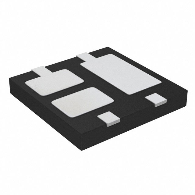
conduction loss. It is housed in a UDFN 3.0 x 3.0 x 0.5 mm package
that is ideal for space constrained wireless applications.
www.onsemi.com
Features
• Extremely Fast Switching Speed
• Low Forward Voltage − 0.49 V (Typ) @ IF = 1 A
• These Devices are Pb−Free, Halogen Free and are RoHS Compliant
MARKING
DIAGRAM
1
• Low Voltage Full Bridge Rectification & Wireless Charging
Reverse Voltage
Forward Current (DC)
Symbol
Value
Unit
VR
30
V
IF
1.0
A
Forward Current Surge Peak
(60 Hz, 1 cycle)
IFSM
12
A
Non−Repetitive Peak Forward Current
(Square Wave, TJ = 25°C prior to surge)
t = 1 ms
t = 1 ms
t=1s
IFSM
1030
= Specific Device Code
A
= Assembly Location
Y
= Year
WW
= Work Week
G
= Pb−Free Package
(Note: Microdot may be in either location)
A
PIN CONNECTIONS
40
10
3.0
Stresses exceeding those listed in the Maximum Ratings table may damage the
device. If any of these limits are exceeded, device functionality should not be
assumed, damage may occur and reliability may be affected.
1. All specifications pertain to a single diode.
THERMAL CHARACTERISTICS
Characteristic
Symbol
Max
Unit
Total Device Dissipation
TA = 25°C
Derate above 25°C
PD
(Note 2)
1.80
W
18
mW/°C
Thermal Resistance Junction to Ambient
RqJA
(Note 2)
55.5
°C/W
Total Device Dissipation
TA = 25°C
Derate above 25°C
PD
(Note 3)
0.70
W
7.0
mW/°C
Thermal Resistance Junction to Ambient
RqJA
(Note 3)
142
°C/W
Total Device Dissipation
TA = 25°C
Derate above 25°C
PD
(Note 4)
0.80
W
8.0
mW/°C
Device
Package
Shipping†
Thermal Resistance Junction to Ambient
RqJA
(Note 4)
125
°C/W
NSR1030QMUTWG
3000 / Tape &
Reel
Junction Temperature
TJ
+125
°C
UDFN4
(Pb−Free)
Storage Temperature Range
Tstg
−55 to
+150
°C
2. 4 Layer JEDEC JESD51.7 FR−4 @ 10 mm2, 1 oz. copper trace, still air.
3. Single Layer JEDEC JESD51.3 FR−4 @ 100 mm2, 1 oz. copper trace, still air.
4. Single Layer JEDEC JESD51.3 FR−4 @ 100 mm2, 2 oz. copper trace, still air.
© Semiconductor Components Industries, LLC, 2015
May, 2017 − Rev. 1
DEVICE SCHEMATIC
ORDERING INFORMATION
†For information on tape and reel specifications,
including part orientation and tape sizes, please
refer to our Tape and Reel Packaging Specification
Brochure, BRD8011/D.
Publication Order Number:
NSR1030QMU/D
M
MAXIMUM RATINGS (TJ = 125°C unless otherwise noted) (Note 1)
Rating
1030
AYWWG
G
UDFN4 3x3
CASE 517DB
Typical Applications
�NSR1030QMUTWG
ELECTRICAL CHARACTERISTICS (TA = 25°C unless otherwise noted) (Note 5)
Symbol
Min
Typ
Max
Unit
V(BR)
30
−
−
V
Reverse Leakage (VR = 30 V)
IR
−
4.0
20
mA
Forward Voltage (IF = 0.5 A)
VF
−
0.43
0.49
V
Forward Voltage (IF = 1.0 A)
VF
−
0.49
0.60
V
Reverse Recovery Time
(IF = IR = 10 mA, IR(REC) = 1.0 mA)
trr
−
25
−
ns
Input Capacitance (pins 1 to 3) (VR = 1.0 V, f = 1.0 MHz)
CT
−
70
−
pF
Characteristic
Reverse Breakdown Voltage (IR = 1.0 mA)
Product parametric performance is indicated in the Electrical Characteristics for the listed test conditions, unless otherwise noted. Product
performance may not be indicated by the Electrical Characteristics if operated under different conditions.
5. All specifications pertain to a single diode.
820 W
+10 V
2.0 k
100 mH
tr
0.1 mF
IF
tp
t
IF
trr
10%
t
0.1 mF
90%
D.U.T.
50 W OUTPUT
PULSE
GENERATOR
50 W INPUT
SAMPLING
OSCILLOSCOPE
iR(REC) = 1.0 mA
IR
VR
INPUT SIGNAL
OUTPUT PULSE
(IF = IR = 10 mA; MEASURED
at iR(REC) = 1.0 mA)
Notes: 1. A 2.0 kW variable resistor adjusted for a Forward Current (IF) of 10 mA.
Notes: 2. Input pulse is adjusted so IR(peak) is equal to 10 mA.
Notes: 3. tp » trr
Figure 1. Recovery Time Equivalent Test Circuit
www.onsemi.com
2
�NSR1030QMUTWG
TYPICAL CHARACTERISTICS
IR, REVERSE CURRENT (mA)
1.0E−01
0.1
150°C
0.01
0.001
0.0
125°C
0.1
85°C
0.2
1.0E−03
125°C
1.0E−04
85°C
1.0E−05
1.0E−06
1.0E−08
1.0E−09
CI, INPUT CAPACITANCE (pF)
−55°C
1.0E−10
25°C
0.3
−55°C
0.4
0.5
1.0E−11
0
0.6
5
10
15
20
VR, REVERSE VOLTAGE (V)
Figure 1. Forward Voltage
Figure 2. Reverse Leakage
70
60
50
40
30
20
10
15
20
25
30
30
25
VF, FORWARD VOLTAGE (V)
TA = 25°C
5
25°C
1.0E−07
80
0
150°C
1.0E−02
IFSM, FORWARD SURGE MAX CURRENT (A)
IF, FORWARD CURRENT (A)
1
45
Based on square wave currents
TJ = 25°C prior to surge
40
35
30
25
20
15
10
5
0
0.001
0.01
0.1
1
10
100
VR, REVERSE VOLTAGE (V)
Tp, PULSE ON TIME (ms)
Figure 3. Input Capacitance
Figure 4. Forward Surge Current
1000
100
D = 0.5
0.2
10
0.1
r(t)
(°C/W)
0.05
0.02
1
0.01
SINGLE PULSE
0.1
0.000001
0.00001
0.0001
0.001
0.01
0.1
PULSE TIME (s)
Figure 5. Thermal Response
www.onsemi.com
3
1
10
100
1000
�MECHANICAL CASE OUTLINE
PACKAGE DIMENSIONS
UDFN4 3.0x3.0, 1.30P
CASE 517DB
ISSUE A
DATE 17 SEP 2014
SCALE 2:1
D
ÍÍ
ÍÍ
PIN ONE
INDICATOR
2X
0.10 C
2X
0.10 C
NOTES:
1. DIMENSIONING AND TOLERANCING PER
ASME Y14.5M, 1994.
2. CONTROLLING DIMENSION: MILLIMETERS.
3. DIMENSION b APPLIES TO PLATED
TERMINAL AND IS MEASURED BETWEEN
0.05 AND 0.15 MM FROM THE TERMINAL TIP.
4. COPLANARITY APPLIES TO THE EXPOSED
PADS AS WELL AS THE TERMINALS.
5. POSITIONAL TOLERANCE APPLIES TO ALL
OF THE EXPOSED PADS.
A B
E
TOP VIEW
A
DIM
A
A1
A3
b
D
D2
D3
E
E2
E3
E4
e
F
F1
G
L
A3
A1
0.05 C
0.05 C
NOTE 4
C
SIDE VIEW
0.10
2X
D3
C A B
M
F
NOTE 5
D2
1
SEATING
PLANE
F1
2
1
2
4
3
E2
E3
E4
4
4X
0.10
3
L
4X
M
G
NOTE 5
b
BOTTOM VIEW
C A B
0.10
M
C A B
0.05
M
C
e/2
RECOMMENDED
SOLDERING FOOTPRINT*
1.30
PITCH
1.40
1.20
4X
1.17
0.87
1.00 1
0.70
0.75
1
XXXX
AYWWG
G
XXXX = Specific Device Code
A
= Assembly Location
Y
= Year
WW
= Work Week
G
= Pb−Free Package
(Note: Microdot may be in either location)
2X
0.63
0.55
GENERIC
MARKING DIAGRAM*
e
SUPPLEMENTAL
BOTTOM VIEW
NOTE 3
MILLIMETERS
MIN
MAX
0.45
0.55
0.00
0.05
0.13 REF
0.35
0.45
3.00 BSC
0.95
1.05
1.15
1.25
3.00 BSC
1.80
1.90
0.75
0.85
0.65
0.75
1.30 BSC
0.75 BSC
0.70 BSC
0.48 BSC
0.35
0.55
*This information is generic. Please refer
to device data sheet for actual part
marking.
Pb−Free indicator, “G” or microdot “ G”,
may or may not be present.
2.02 3.30
2X
0.50
DIMENSIONS: MILLIMETERS
*For additional information on our Pb−Free strategy and soldering
details, please download the ON Semiconductor Soldering and
Mounting Techniques Reference Manual, SOLDERRM/D.
DOCUMENT NUMBER:
DESCRIPTION:
98AON91435F
UDFN4 3.0X3.0, 1.30P
Electronic versions are uncontrolled except when accessed directly from the Document Repository.
Printed versions are uncontrolled except when stamped “CONTROLLED COPY” in red.
PAGE 1 OF 1
ON Semiconductor and
are trademarks of Semiconductor Components Industries, LLC dba ON Semiconductor or its subsidiaries in the United States and/or other countries.
ON Semiconductor reserves the right to make changes without further notice to any products herein. ON Semiconductor makes no warranty, representation or guarantee regarding
the suitability of its products for any particular purpose, nor does ON Semiconductor assume any liability arising out of the application or use of any product or circuit, and specifically
disclaims any and all liability, including without limitation special, consequential or incidental damages. ON Semiconductor does not convey any license under its patent rights nor the
rights of others.
© Semiconductor Components Industries, LLC, 2019
www.onsemi.com
�onsemi,
, and other names, marks, and brands are registered and/or common law trademarks of Semiconductor Components Industries, LLC dba “onsemi” or its affiliates
and/or subsidiaries in the United States and/or other countries. onsemi owns the rights to a number of patents, trademarks, copyrights, trade secrets, and other intellectual property.
A listing of onsemi’s product/patent coverage may be accessed at www.onsemi.com/site/pdf/Patent−Marking.pdf. onsemi reserves the right to make changes at any time to any
products or information herein, without notice. The information herein is provided “as−is” and onsemi makes no warranty, representation or guarantee regarding the accuracy of the
information, product features, availability, functionality, or suitability of its products for any particular purpose, nor does onsemi assume any liability arising out of the application or use
of any product or circuit, and specifically disclaims any and all liability, including without limitation special, consequential or incidental damages. Buyer is responsible for its products
and applications using onsemi products, including compliance with all laws, regulations and safety requirements or standards, regardless of any support or applications information
provided by onsemi. “Typical” parameters which may be provided in onsemi data sheets and/or specifications can and do vary in different applications and actual performance may
vary over time. All operating parameters, including “Typicals” must be validated for each customer application by customer’s technical experts. onsemi does not convey any license
under any of its intellectual property rights nor the rights of others. onsemi products are not designed, intended, or authorized for use as a critical component in life support systems
or any FDA Class 3 medical devices or medical devices with a same or similar classification in a foreign jurisdiction or any devices intended for implantation in the human body. Should
Buyer purchase or use onsemi products for any such unintended or unauthorized application, Buyer shall indemnify and hold onsemi and its officers, employees, subsidiaries, affiliates,
and distributors harmless against all claims, costs, damages, and expenses, and reasonable attorney fees arising out of, directly or indirectly, any claim of personal injury or death
associated with such unintended or unauthorized use, even if such claim alleges that onsemi was negligent regarding the design or manufacture of the part. onsemi is an Equal
Opportunity/Affirmative Action Employer. This literature is subject to all applicable copyright laws and is not for resale in any manner.
PUBLICATION ORDERING INFORMATION
LITERATURE FULFILLMENT:
Email Requests to: orderlit@onsemi.com
onsemi Website: www.onsemi.com
◊
TECHNICAL SUPPORT
North American Technical Support:
Voice Mail: 1 800−282−9855 Toll Free USA/Canada
Phone: 011 421 33 790 2910
Europe, Middle East and Africa Technical Support:
Phone: 00421 33 790 2910
For additional information, please contact your local Sales Representative
�


 工商网监
湘ICP备2023018690号
工商网监
湘ICP备2023018690号
