NST847BPDP6T5G
Dual Complementary
General Purpose Transistor
The NST847BPDP6T5G device is a spin−off of our popular
SOT−23/SOT−323/SOT−563 three−leaded device. It is designed for
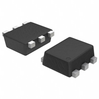
general purpose amplifier applications and is housed in the SOT−963
six−leaded surface mount package. By putting two discrete devices in
one package, this device is ideal for low−power surface mount
applications where board space is at a premium.
(3)
Features
•
•
•
•
•
•
www.onsemi.com
hFE, 200−450
Low VCE(sat), ≤ 0.3 V
Simplifies Circuit Design
Reduces Board Space
Reduces Component Count
This is a Pb−Free Device
(2)
Q1
Q2
(4)
(5)
(6)
NST847BPDP6T5G*
*Q1 PNP
Q2 NPN
MAXIMUM RATINGS
Rating
Symbol
Value
Unit
Collector −Emitter Voltage
VCEO
45
Vdc
Collector −Base Voltage
VCBO
50
Vdc
Emitter −Base Voltage
VEBO
6.0
Vdc
IC
100
mAdc
ESD
Class
2
B
Symbol
Max
Unit
PD
240
1.9
mW
mW/°C
RqJA
520
°C/W
PD
280
2.2
mW
mW/°C
Thermal Resistance, Junction-to-Ambient
(Note 2)
RqJA
446
°C/W
Characteristic (Dual Heated) (Note 3)
Symbol
Max
Unit
PD
350
2.8
mW
mW/°C
RqJA
357
°C/W
PD
420
3.4
mW
mW/°C
Thermal Resistance, Junction-to-Ambient
(Note 2)
RqJA
297
°C/W
Junction and Storage Temperature Range
TJ, Tstg
−55 to
+150
°C
Collector Current − Continuous
Electrostatic Discharge
(1)
HBM
MM
SOT−963
CASE 527AD
THERMAL CHARACTERISTICS
Characteristic (Single Heated)
Total Device Dissipation TA = 25°C
Derate above 25°C (Note 1)
Thermal Resistance, Junction-to-Ambient
(Note 1)
Total Device Dissipation TA = 25°C
Derate above 25°C (Note 2)
Total Device Dissipation TA = 25°C
Derate above 25°C (Note 1)
Thermal Resistance, Junction-to-Ambient
(Note 1)
Total Device Dissipation TA = 25°C
Derate above 25°C (Note 2)
MARKING DIAGRAM
AM
1
A
M
= Device Code
= Date Code
ORDERING INFORMATION
Device
Package
NST847BPDP6T5G SOT−963
(Pb−Free)
Shipping†
8000/Tape & Reel
†For information on tape and reel specifications,
including part orientation and tape sizes, please
refer to our Tape and Reel Packaging Specifications
Brochure, BRD8011/D.
Stresses exceeding those listed in the Maximum Ratings table may damage the
device. If any of these limits are exceeded, device functionality should not be
assumed, damage may occur and reliability may be affected.
1. FR−4 @ 100 mm2, 1 oz. copper traces, still air.
2. FR−4 @ 500 mm2, 1 oz. copper traces, still air.
3. Dual heated values assume total power is sum of two equally powered channels
© Semiconductor Components Industries, LLC, 2008
June, 2017 − Rev. 1
1
Publication Order Number:
NST847BPDP6/D
�NST847BPDP6T5G
ELECTRICAL CHARACTERISTICS (TA = 25°C unless otherwise noted)
Symbol
Min
Typ
Max
45
−45
−
−
−
−
50
−50
−
−
−
−
50
−50
−
−
−
−
6.0
−5.0
−
−
−
−
−
−
−
−
−
−
−
−
15
5.0
−15
−4.0
200
290
450
220
290
475
−
−
−
−
0.25
0.60
−
−
−
−
−0.30
−0.70
−
−
0.70
0.90
−
−
−
−
−0.70
−0.90
−
−
0.58
−
0.66
−
0.70
0.77
−0.60
−
−
−
−0.75
−0.82
100
−
−
100
−
−
−
−
4.5
−
−
4.5
(NPN)
−
−
10
(PNP)
−
−
10
Characteristic
Unit
OFF CHARACTERISTICS
Collector −Emitter Breakdown Voltage
(IC = 1.0 mA, IB = 0)
(IC = −1.0 mA, IB = 0)
(NPN)
(PNP)
Collector −Base Breakdown Voltage
(IC = 10 mA, IE = 0)
(IC = −10 mA, IE = 0)
(NPN)
(PNP)
Collector −Emitter Breakdown Voltage
(IC = 10 mA)
(IC = −10 mA)
(NPN)
(PNP)
Emitter −Base Breakdown Voltage
(IE = 1.0 mA, IC = 0)
(IE = −1.0 mA, IC = 0)
(NPN)
(PNP)
Collector Cutoff Current
(VCB = 30 V)
(VCB = 30 V, TA = 150°C)
(VCB = −30 V)
(VCB = −30 V, TA = 150°C)
(NPN)
(NPN)
(PNP)
(PNP)
V(BR)CEO
V(BR)CBO
V(BR)CES
V(BR)EBO
ICBO
V
V
V
V
nA
mA
nA
mA
ON CHARACTERISTICS (Note 4)
DC Current Gain
(IC = 2.0 mA, VCE = 5.0 V)
(NPN)
(IC = −2.0 mA, VCE = −5.0 V)
hFE
(PNP)
Collector −Emitter Saturation Voltage
(IC = 10 mA, IB = 0.5 mA)
(IC = 100 mA, IB = 5.0 mA)
(NPN)
(IC = −10 mA, IB = −0.5 mA)
(IC = −100 mA, IB = −5.0 mA)
VCE(sat)
(PNP)
Base −Emitter Saturation Voltage
(IC = 10 mA, IB = 0.5 mA)
(IC = 100 mA, IB = 5.0 mA)
(NPN)
(IC = −10 mA, IB = −0.5 mA)
(IC = −100 mA, IB = −5.0 mA)
VBE(sat)
(PNP)
Base −Emitter On Voltage
(IC = 2.0 mA, VCE = 5.0 V)
(IC = 10 mA, VCE = 5.0 V)
(NPN)
(IC = −2.0 mA, VCE = −5.0 V)
(IC = −10 mA, VCE = −5.0 V)
VBE(on)
(PNP)
−
V
V
V
SMALL−SIGNAL CHARACTERISTICS
Current−Gain − Bandwidth Product
(IC = 10 mA, VCE = 5.0 V, f = 100 MHz)
(NPN)
(IC = −10 mA, VCE = −5.0 V, f = 100 MHz)
fT
(PNP)
Output Capacitance
(VCB = 10 V, f = 1.0 MHz)
(NPN)
(VCB = −10 V, f = 1.0 MHz)
Cob
(PNP)
Noise Figure
(IC = 0.2 mA, VCE = 5.0 V, RS = 2 kW, f = 1 kHz, BW = 200 Hz)
MHz
pF
NF
(IC = −0.2 mA, VCE = −5.0 V, RS = 2 kW, f = 1 kHz, BW = 200 Hz)
4. Pulse Test: Pulse Width ≤ 300 μs; Duty Cycle ≤ 2.0%.
www.onsemi.com
2
dB
�NST847BPDP6T5G
NPN TRANSISTOR
0.16
600
150°C (5.0 V)
IC/IB = 10
hFE, DC CURRENT GAIN (V)
VCE(sat), COLLECTOR−EMITTER
SATURATION VOLTAGE (V)
0.18
0.14
0.12
VCE(sat) = 150°C
0.10
0.08
25°C
0.06
0.04
0.02
0.0001
500
150°C (1.0 V)
400
25°C (5.0 V)
300
25°C (1.0 V)
200 −55°C (5.0 V)
100
−55°C (1.0 V)
−55°C
0.001
0.01
IC, COLLECTOR CURRENT (A)
0.1
Figure 1. Collector Emitter Saturation Voltage vs.
Collector Current
0
0.0001
0.001
0.01
IC, COLLECTOR CURRENT (A)
0.1
Figure 2. DC Current Gain vs. Collector Current
NPN TRANSISTOR
www.onsemi.com
3
�NST847BPDP6T5G
1.0
0.8
VBE(on), BASE−EMITTER TURN−ON
VOLTAGE (V)
0.9
IC/IB = 10
−55°C
0.7
0.6
25°C
0.5
0.4 150°C
0.3
0.0001
0.001
0.01
0.1
−55°C
0.8
0.7
25°C
0.6
0.5
0.4 150°C
0.3
0.0001
0.001
0.01
0.1
IC, COLLECTOR CURRENT (A)
Figure 3. Base Emitter Saturation Voltage vs.
Collector Current
Figure 4. Base Emitter Turn−On Voltage vs.
Collector Current
1.0
7.0
IC = 100 mA
0.9
0.8
0.7
50 mA
0.6
0.5
0.4
30 mA
0.3
0.2
0.1
0
0.00001
10 mA
0.0001
0.001
0.01
6.5
6.0
5.5
5.0
Cib
4.5
4.0
3.5
3.0
0
0.5
1.0
1.5
2.0
2.5
3.0
3.5
4.0
Ib, BASE CURRENT (A)
Veb, EMITTER BASE VOLTAGE (V)
Figure 5. Saturation Region
Figure 6. Input Capacitance
2.5
Cobo, OUTPUT CAPACITANCE (pF)
VCE(sat), COLLECTOR−EMITTER
SATURATION VOLTAGE (V)
VCE = 2.0 V
0.9
IC, COLLECTOR CURRENT (A)
Cibo, INPUT CAPACITANCE (pF)
VBE(sat), BASE−EMITTER
SATURATION VOLTAGE (V)
1.0
2.3
2.1
1.9
1.7
1.5
1.3
1.1
Cob
0.9
0.7
0
5
10
15
20
25
Vcb, COLLECTOR BASE VOLTAGE (V)
Figure 7. Output Capacitance
www.onsemi.com
4
30
4.5 5.0
�NST847BPDP6T5G
PNP TRANSISTOR
0.16
800
IC/IB = 10
0.14
hFE, DC CURRENT GAIN (V)
VCE(sat), COLLECTOR−EMITTER
SATURATION VOLTAGE (V)
0.18
VCE(sat) = 150°C
0.12
0.10
0.08
25°C
0.06
0.04
0.02
0.0001
−55°C
0.001
0.01
IC, COLLECTOR CURRENT (A)
0.1
Figure 8. Collector Emitter Saturation Voltage vs.
Collector Current
150°C (5.0 V)
700
600
150°C (1.0 V)
500
25°C (5.0 V)
400
300
200
100
25°C (1.0 V)
−55°C (5.0 V)
−55°C (1.0 V)
0
0.0001
0.001
0.01
IC, COLLECTOR CURRENT (A)
0.1
Figure 9. DC Current Gain vs. Collector Current
PNP TRANSISTOR
www.onsemi.com
5
�NST847BPDP6T5G
1.0
0.8
VBE(on), BASE−EMITTER TURN−ON
VOLTAGE (V)
0.9
IC/IB = 10
−55°C
0.7
0.6
25°C
0.5
0.4 150°C
0.3
0.0001
0.001
0.01
VCE = 2.0 V
0.9
−55°C
0.8
0.7
25°C
0.6
0.5
0.4
150°C
0.3
0.0001
0.001
0.01
0.1
IC, COLLECTOR CURRENT (A)
IC, COLLECTOR CURRENT (A)
Figure 10. Base Emitter Saturation Voltage vs.
Collector Current
Figure 11. Base Emitter Turn−On Voltage vs.
Collector Current
1.0
10
IC =
100 mA
0.9
0.8
0.7
50 mA
0.6
0.5
30 mA
0.4
0.3
0.2
0.1
0
0.00001
10 mA
0.0001
0.001
0.01
9
8
7
6
Cib
5
4
3
0
1.0
2.0
3.0
4.0
Ib, BASE CURRENT (A)
Veb, EMITTER BASE VOLTAGE (V)
Figure 12. Saturation Region
Figure 13. Input Capacitance
4.5
Cobo, OUTPUT CAPACITANCE (pF)
VCE(sat), COLLECTOR−EMITTER
SATURATION VOLTAGE (V)
0.1
Cibo, INPUT CAPACITANCE (pF)
VBE(sat), BASE−EMITTER
SATURATION VOLTAGE (V)
1.0
4.0
3.5
3.0
2.5
2.0
1.5
Cob
1.0
0.5
0
5
10
15
20
25
Vcb, COLLECTOR BASE VOLTAGE (V)
Figure 14. Output Capacitance
www.onsemi.com
6
30
5.0
�MECHANICAL CASE OUTLINE
PACKAGE DIMENSIONS
SOT−963
CASE 527AD−01
ISSUE E
DATE 09 FEB 2010
SCALE 4:1
D
X
Y
6
5
4
1
2
3
A
HE
E
NOTES:
1. DIMENSIONING AND TOLERANCING PER ASME
Y14.5M, 1994.
2. CONTROLLING DIMENSION: MILLIMETERS
3. MAXIMUM LEAD THICKNESS INCLUDES LEAD
FINISH THICKNESS. MINIMUM LEAD
THICKNESS IS THE MINIMUM THICKNESS OF
BASE MATERIAL.
4. DIMENSIONS D AND E DO NOT INCLUDE MOLD
FLASH, PROTRUSIONS, OR GATE BURRS.
DIM
A
b
C
D
E
e
HE
L
L2
C
SIDE VIEW
TOP VIEW
e
6X
6X L2
6X
BOTTOM VIEW
L
MILLIMETERS
MIN
NOM
MAX
0.34
0.37
0.40
0.10
0.15
0.20
0.07
0.12
0.17
0.95
1.00
1.05
0.75
0.80
0.85
0.35 BSC
0.95
1.00
1.05
0.19 REF
0.05
0.10
0.15
GENERIC
MARKING DIAGRAM*
b
0.08 X Y
XM
1
STYLE 1:
PIN 1. EMITTER 1
2. BASE 1
3. COLLECTOR 2
4. EMITTER 2
5. BASE 2
6. COLLECTOR 1
STYLE 2:
PIN 1. EMITTER 1
2. EMITTER2
3. BASE 2
4. COLLECTOR 2
5. BASE 1
6. COLLECTOR 1
STYLE 3:
PIN 1. CATHODE 1
2. CATHODE 1
3. ANODE/ANODE 2
4. CATHODE 2
5. CATHODE 2
6. ANODE/ANODE 1
STYLE 4:
PIN 1. COLLECTOR
2. COLLECTOR
3. BASE
4. EMITTER
5. COLLECTOR
6. COLLECTOR
STYLE 5:
PIN 1. CATHODE
2. CATHODE
3. ANODE
4. ANODE
5. CATHODE
6. CATHODE
STYLE 6:
PIN 1. CATHODE
2. ANODE
3. CATHODE
4. CATHODE
5. CATHODE
6. CATHODE
STYLE 7:
PIN 1. CATHODE
2. ANODE
3. CATHODE
4. CATHODE
5. ANODE
6. CATHODE
STYLE 8:
PIN 1. DRAIN
2. DRAIN
3. GATE
4. SOURCE
5. DRAIN
6. DRAIN
STYLE 9:
PIN 1. SOURCE 1
2. GATE 1
3. DRAIN 2
4. SOURCE 2
5. GATE 2
6. DRAIN 1
STYLE 10:
PIN 1. CATHODE 1
2. N/C
3. CATHODE 2
4. ANODE 2
5. N/C
6. ANODE 1
DOCUMENT NUMBER:
DESCRIPTION:
X
M
= Specific Device Code
= Month Code
*This information is generic. Please refer
to device data sheet for actual part
marking.
Pb−Free indicator, “G” or microdot “ G”,
may or may not be present.
RECOMMENDED
MOUNTING FOOTPRINT
6X
0.20
6X
0.35
PACKAGE
OUTLINE
1.20
0.35
PITCH
DIMENSIONS: MILLIMETERS
98AON26456D
SOT−963, 1X1, 0.35P
Electronic versions are uncontrolled except when accessed directly from the Document Repository.
Printed versions are uncontrolled except when stamped “CONTROLLED COPY” in red.
PAGE 1 OF 1
ON Semiconductor and
are trademarks of Semiconductor Components Industries, LLC dba ON Semiconductor or its subsidiaries in the United States and/or other countries.
ON Semiconductor reserves the right to make changes without further notice to any products herein. ON Semiconductor makes no warranty, representation or guarantee regarding
the suitability of its products for any particular purpose, nor does ON Semiconductor assume any liability arising out of the application or use of any product or circuit, and specifically
disclaims any and all liability, including without limitation special, consequential or incidental damages. ON Semiconductor does not convey any license under its patent rights nor the
rights of others.
© Semiconductor Components Industries, LLC, 2019
www.onsemi.com
�onsemi,
, and other names, marks, and brands are registered and/or common law trademarks of Semiconductor Components Industries, LLC dba “onsemi” or its affiliates
and/or subsidiaries in the United States and/or other countries. onsemi owns the rights to a number of patents, trademarks, copyrights, trade secrets, and other intellectual property.
A listing of onsemi’s product/patent coverage may be accessed at www.onsemi.com/site/pdf/Patent−Marking.pdf. onsemi reserves the right to make changes at any time to any
products or information herein, without notice. The information herein is provided “as−is” and onsemi makes no warranty, representation or guarantee regarding the accuracy of the
information, product features, availability, functionality, or suitability of its products for any particular purpose, nor does onsemi assume any liability arising out of the application or use
of any product or circuit, and specifically disclaims any and all liability, including without limitation special, consequential or incidental damages. Buyer is responsible for its products
and applications using onsemi products, including compliance with all laws, regulations and safety requirements or standards, regardless of any support or applications information
provided by onsemi. “Typical” parameters which may be provided in onsemi data sheets and/or specifications can and do vary in different applications and actual performance may
vary over time. All operating parameters, including “Typicals” must be validated for each customer application by customer’s technical experts. onsemi does not convey any license
under any of its intellectual property rights nor the rights of others. onsemi products are not designed, intended, or authorized for use as a critical component in life support systems
or any FDA Class 3 medical devices or medical devices with a same or similar classification in a foreign jurisdiction or any devices intended for implantation in the human body. Should
Buyer purchase or use onsemi products for any such unintended or unauthorized application, Buyer shall indemnify and hold onsemi and its officers, employees, subsidiaries, affiliates,
and distributors harmless against all claims, costs, damages, and expenses, and reasonable attorney fees arising out of, directly or indirectly, any claim of personal injury or death
associated with such unintended or unauthorized use, even if such claim alleges that onsemi was negligent regarding the design or manufacture of the part. onsemi is an Equal
Opportunity/Affirmative Action Employer. This literature is subject to all applicable copyright laws and is not for resale in any manner.
PUBLICATION ORDERING INFORMATION
LITERATURE FULFILLMENT:
Email Requests to: orderlit@onsemi.com
onsemi Website: www.onsemi.com
◊
TECHNICAL SUPPORT
North American Technical Support:
Voice Mail: 1 800−282−9855 Toll Free USA/Canada
Phone: 011 421 33 790 2910
Europe, Middle East and Africa Technical Support:
Phone: 00421 33 790 2910
For additional information, please contact your local Sales Representative
�