NSVP249SDSF3
PIN Diode
Dual series PIN Diode for
VHF, UHF and AGC
www.onsemi.com
This PIN diode is designed to realize compact and efficient designs.
Two PIN diodes are incorporated in one SC−70 package. The use of
dual PIN diodes can reduce both system cost and board space. This
PIN diode is AEC−Q101 qualified and PPAP capable for automotive
applications.
50 V, 50 mA
rs = 4.5 W max
PIN Diode
Features
•
•
•
•
•
ELECTRICAL CONECTION
Series connection of 2 elements in a small−size package
Small Interterminal Capacitance (C = 0.23 pF typ)
Small Forward Series Resistance (rs = 4.5 W max)
AEC−Q101 qualified and PPAP capable
Pb−Free, Halogen Free and RoHS Compliance
1 : Anode
2 : Cathode
3 : Cathode / Anode
Typical Applications
• Auto Gain Control for Radio
MARKING
DIAGRAM
SPECIFICATIONS
ABSOLUTE MAXIMUM RATINGS at TA = 25°C
Symbol
Parameter
Value
Unit
VR
Reverse Voltage
50
V
IF
Forward Current
50
mA
P
Allowable Power Dissipation
100
mW
−55 to +125
°C
TJ, Tstg
Operating Junction and Storage
Temperature
Stresses exceeding those listed in the Maximum Ratings table may damage the
device. If any of these limits are exceeded, device functionality should not be
assumed, damage may occur and reliability may be affected.
3
1
2
MCP3
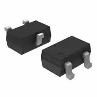
CASE 419 AJ
ORDERING INFORMATION
See detailed ordering and shipping information on
page 3 of this data sheet
ELECTRICAL CHARACTERISTICS at TA = 25°C (Note 1)
Parameter
Symbol
Conditions
Min
Typ
Max
Unit
VR
Reverse Voltage
IR = 10 mA
50
−
−
V
IR
Reverse Current
VR = 50 V
−
−
0.1
mA
VF
Forward Voltage
IF = 50 mA
−
0.92
−
V
C
Interterminal Capacitance
VR = 50 V, f = 1 MHz
−
0.23
−
pF
rs
Series Resistance
IF = 10 mA, f = 100 MHz
−
−
4.5
W
Product parametric performance is indicated in the Electrical Characteristics for the listed test conditions, unless otherwise noted. Product
performance may not be indicated by the Electrical Characteristics if operated under different conditions.
1. The specifications shown above are for each individual diode.
© Semiconductor Components Industries, LLC, 2018
February, 2018 − Rev. 0
1
Publication Order Number:
NSVP249SDSF3/D
�NSVP249SDSF3
0.1
5
Interterminal Capacitance, C −pF
Forward Current, IF − mA
3
2
10
7
5
3
2
TA = 125°C
1.0
7
5
3
2
0.1
7
5
3
2
0.01
−55°C
25°C
0
0.2
0.4
0.6
0.8
1.0
5
3
2
0.1
0.1
1.2
2
3
5 7 1.0
2
3
5 7 10
2
Forward Voltage, VF − V
Reverse Voltage, VR − V
Figure 1. IF −VF
Figure 2. C −VR
5
3
3
5 7 100
TA = 25°C
IF = 10 mA
1000
7
5
5
Series Resistance, rs − W
7
3
2
3
2
TA = 75°C
10
Reverse Current, IR − nA
7
5
2
TA = 25°C
f = 1 MHz
50°C
1.0
7
5
3
100 mA
2
100
7
5
3
1 mA
3
2
2
25°C
0.1
10
7
7
5
5
3
3
2
10 mA
2
0
10
20
30
40
50
60
Reverse Voltage, VR − V
0
2 3
5 7 10
2 3
5 7 100
2 3
Frequency, f − MHz
Figure 3. IR −VR
Figure 4. rs − f
www.onsemi.com
2
5 7 1000
2
�NSVP249SDSF3
1k
7
5
TA = 25°C
f = 100 MHz
3
Resistance, rs − W
2
100
7
5
3
2
10
7
5
3
2
1.0
0.01
2
3
5 7 0.1
2
3
5 7 1.0
2
3
5 7 10
Forward Reverse, IF − mA
Figure 5. rs − IF
ORDERING INFORMATION
Device
NSVP249SDSF3T1G
Marking
Package
Shipping †
GV
SC−70 / MCP3
(Pb−Free / Halogen Free)
3,000 / Tape & Reel
†For information on tape and reel specifications, including part orientation and tape sizes, please refer to our Tape and Reel Packaging
Specifications Brochure, BRD8011/D.
www.onsemi.com
3
�MECHANICAL CASE OUTLINE
PACKAGE DIMENSIONS
SC−70 / MCP3
CASE 419AJ
ISSUE O
DOCUMENT NUMBER:
98AON65442E
DESCRIPTION:
SC−70 / MCP3
DATE 30 NOV 2011
Electronic versions are uncontrolled except when accessed directly from the Document Repository.
Printed versions are uncontrolled except when stamped “CONTROLLED COPY” in red.
PAGE 1 OF 1
ON Semiconductor and
are trademarks of Semiconductor Components Industries, LLC dba ON Semiconductor or its subsidiaries in the United States and/or other countries.
ON Semiconductor reserves the right to make changes without further notice to any products herein. ON Semiconductor makes no warranty, representation or guarantee regarding
the suitability of its products for any particular purpose, nor does ON Semiconductor assume any liability arising out of the application or use of any product or circuit, and specifically
disclaims any and all liability, including without limitation special, consequential or incidental damages. ON Semiconductor does not convey any license under its patent rights nor the
rights of others.
© Semiconductor Components Industries, LLC, 2019
www.onsemi.com
�onsemi,
, and other names, marks, and brands are registered and/or common law trademarks of Semiconductor Components Industries, LLC dba “onsemi” or its affiliates
and/or subsidiaries in the United States and/or other countries. onsemi owns the rights to a number of patents, trademarks, copyrights, trade secrets, and other intellectual property.
A listing of onsemi’s product/patent coverage may be accessed at www.onsemi.com/site/pdf/Patent−Marking.pdf. onsemi reserves the right to make changes at any time to any
products or information herein, without notice. The information herein is provided “as−is” and onsemi makes no warranty, representation or guarantee regarding the accuracy of the
information, product features, availability, functionality, or suitability of its products for any particular purpose, nor does onsemi assume any liability arising out of the application or use
of any product or circuit, and specifically disclaims any and all liability, including without limitation special, consequential or incidental damages. Buyer is responsible for its products
and applications using onsemi products, including compliance with all laws, regulations and safety requirements or standards, regardless of any support or applications information
provided by onsemi. “Typical” parameters which may be provided in onsemi data sheets and/or specifications can and do vary in different applications and actual performance may
vary over time. All operating parameters, including “Typicals” must be validated for each customer application by customer’s technical experts. onsemi does not convey any license
under any of its intellectual property rights nor the rights of others. onsemi products are not designed, intended, or authorized for use as a critical component in life support systems
or any FDA Class 3 medical devices or medical devices with a same or similar classification in a foreign jurisdiction or any devices intended for implantation in the human body. Should
Buyer purchase or use onsemi products for any such unintended or unauthorized application, Buyer shall indemnify and hold onsemi and its officers, employees, subsidiaries, affiliates,
and distributors harmless against all claims, costs, damages, and expenses, and reasonable attorney fees arising out of, directly or indirectly, any claim of personal injury or death
associated with such unintended or unauthorized use, even if such claim alleges that onsemi was negligent regarding the design or manufacture of the part. onsemi is an Equal
Opportunity/Affirmative Action Employer. This literature is subject to all applicable copyright laws and is not for resale in any manner.
ADDITIONAL INFORMATION
TECHNICAL PUBLICATIONS:
Technical Library: www.onsemi.com/design/resources/technical−documentation
onsemi Website: www.onsemi.com
ONLINE SUPPORT: www.onsemi.com/support
For additional information, please contact your local Sales Representative at
www.onsemi.com/support/sales
�


 工商网监
湘ICP备2023018690号
工商网监
湘ICP备2023018690号
