DATA SHEET
www.onsemi.com
Dual Common
Base-Collector Bias
Resistor Transistors
NPN and PNP Silicon Surface Mount
Transistors with Monolithic Bias
Resistor Network
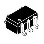
SC−88A/SOT−353
CASE 419A
STYLE 6
3
UMC2NT1G,
NSVUMC2NT1G,
UMC3NT1G,
NSVUMC3NT1G,
UMC5NT1G/T2G,
NSVUMC5NT1G/T2G
R1
R2
Q2
Q1
R1
4
Features
•
1
R2
The Bias Resistor Transistor (BRT) contains a single transistor with
a monolithic bias network consisting of two resistors; a series base
resistor and a base−emitter resistor. These digital transistors are
designed to replace a single device and its external resistor bias
network. The BRT eliminates these individual components by
integrating them into a single device. In the UMC2NT1G series, two
complementary BRT devices are housed in the SOT−353 package
which is ideal for low power surface mount applications where board
space is at a premium.
•
•
•
•
•
2
Simplifies Circuit Design
Reduces Board Space
Reduces Component Count
Available in 8 mm, 7 inch/3000 Unit Tape and Reel
NSV Prefix for Automotive and Other Applications Requiring
Unique Site and Control Change Requirements; AEC−Q101
Qualified and PPAP Capable
These Devices are Pb−Free, Halogen Free/BFR Free and are RoHS
Compliant*
5
MARKING DIAGRAM
5
4
Ux M G
G
1
2
3
Ux
= Device Marking
x
= 2, 3 or 5
M
= Date Code
G
= Pb−Free Package
(Note: Microdot may be in either location)
ORDERING INFORMATION
See detailed ordering and shipping information in the package
dimensions section on page 4 of this data sheet.
MAXIMUM RATINGS (TA = 25°C unless otherwise noted, common for
Q1 and Q2, − minus sign for Q1 (PNP) omitted)
Rating
Symbol
Value
Unit
Collector-Base Voltage
VCBO
50
Vdc
Collector-Emitter Voltage
VCEO
50
Vdc
IC
100
mAdc
Collector Current
Stresses exceeding those listed in the Maximum Ratings table may damage the
device. If any of these limits are exceeded, device functionality should not be
assumed, damage may occur and reliability may be affected.
*For additional information on our Pb−Free strategy and soldering details, please
download the onsemi Soldering and Mounting Techniques Reference Manual,
SOLDERRM/D.
© Semiconductor Components Industries, LLC, 2011
July, 2022 − Rev. 12
1
Publication Order Number:
UMC2NT1/D
�UMC2NT1G, NSVUMC2NT1G, UMC3NT1G, NSVUMC3NT1G, UMC5NT1G/T2G,
NSVUMC5NT1G/T2G
MAXIMUM RATINGS (TA = 25°C unless otherwise noted, common for Q1 and Q2, − minus sign for Q1 (PNP) omitted)
Rating
Symbol
Value
Unit
RqJA
833
°C/W
TJ, Tstg
−65 to +150
°C
PD
*150
mW
THERMAL CHARACTERISTICS
Thermal Resistance − Junction-to-Ambient (surface mounted)
Operating and Storage Temperature Range
Total Package Dissipation @ TA = 25°C (Note 1)
1. Device mounted on a FR-4 glass epoxy printed circuit board using the minimum recommended footprint.
ELECTRICAL CHARACTERISTICS (TA = 25°C unless otherwise noted)
Characteristic
Symbol
Min
Typ
Max
−
−
100
−
−
500
Unit
Q1 TRANSISTOR: PNP
OFF CHARACTERISTICS
Collector-Base Cutoff Current
(VCB = 50 V, IE = 0)
ICBO
Collector-Emitter Cutoff Current
(VCE = 50 V, IB = 0)
ICEO
Emitter-Base Cutoff Current
(VEB = 6.0, IC = 0 mA)
UMC2NT1G, NSVUMC2NT1G
UMC3NT1G, NSVUMC3NT1G
UMC5NT1G/T2G, NSVUMC5NT1G/T2G
IEBO
nAdc
nAdc
mAdc
−
−
−
−
−
−
0.2
0.5
1.0
50
−
−
50
−
−
60
35
20
100
60
35
−
−
−
−
−
0.25
−
−
0.2
4.9
−
−
15.4
7.0
3.3
22
10
4.7
28.6
13
6.1
0.8
0.8
0.38
1.0
1.0
0.47
1.2
1.2
0.56
ON CHARACTERISTICS
Collector-Base Breakdown Voltage
(IC = 10 mA, IE = 0)
V(BR)CBO
Collector-Emitter Breakdown Voltage
(IC = 2.0 mA, IB = 0)
V(BR)CEO
DC Current Gain
(VCE = 10 V, IC = 5.0 mA)
UMC2NT1G, NSVUMC2NT1G
UMC3NT1G, NSVUMC3NT1G
UMC5NT1G/T2G, NSVUMC5NT1G/T2G
Vdc
Vdc
hFE
Collector−Emitter Saturation Voltage
(IC = 10 mA, IB = 0.3 mA)
VCE(SAT)
Output Voltage (on)
(VCC = 5.0 V, VB = 2.5 V, RL = 1.0 kW)
VOL
Output Voltage (off)
(VCC = 5.0 V, VB = 0.5 V, RL = 1.0 kW)
VOH
Input Resistor
UMC2NT1G
UMC3NT1G
UMC5NT1G/T2G
R1
Resistor Ratio
UMC2NT1G
UMC3NT1G
UMC5NT1G/T2G
R1/R2
www.onsemi.com
2
Vdc
Vdc
Vdc
kW
�UMC2NT1G, NSVUMC2NT1G, UMC3NT1G, NSVUMC3NT1G, UMC5NT1G/T2G,
NSVUMC5NT1G/T2G
ELECTRICAL CHARACTERISTICS (TA = 25°C unless otherwise noted)
Characteristic
Symbol
Min
Typ
Max
−
−
100
−
−
500
Unit
Q2 TRANSISTOR: NPN
OFF CHARACTERISTICS
Collector-Base Cutoff Current
(VCB = 50 V, IE = 0)
ICBO
Collector-Emitter Cutoff Current
(VCE = 50 V, IB = 0)
ICEO
Emitter-Base Cutoff Current
(VEB = 6.0, IC = 0 mA)
UMC2NT1G
UMC3NT1G
UMC5NT1G/T2G
IEBO
nAdc
nAdc
mAdc
−
−
−
−
−
−
0.2
0.5
0.1
50
−
−
50
−
−
60
35
80
100
60
140
−
−
−
−
−
0.25
−
−
0.2
4.9
−
−
15.4
7.0
33
22
10
47
28.6
13
61
0.8
0.8
0.8
1.0
1.0
1.0
1.2
1.2
1.2
ON CHARACTERISTICS
Collector-Base Breakdown Voltage
(IC = 10 mA, IE = 0)
V(BR)CBO
Collector-Emitter Breakdown Voltage
(IC = 2.0 mA, IB = 0)
V(BR)CEO
DC Current Gain
(VCE = 10 V, IC = 5.0 mA)
UMC2NT1G
UMC3NT1G
UMC5NT1G/T2G
Vdc
Vdc
hFE
Collector−Emitter Saturation Voltage
(IC = 10 mA, IB = 0.3 mA)
VCE(SAT)
Output Voltage (on)
(VCC = 5.0 V, VB = 3.5 V, RL = 1.0 kW)
VOL
Output Voltage (off)
(VCC = 5.0 V, VB = 0.5 V, RL = 1.0 kW)
VOH
Input Resistor
UMC2NT1G
UMC3NT1G
UMC5NT1G/T2G
R1
Resistor Ratio
UMC2NT1G
UMC3NT1G
UMC5NT1G/T2G
R1/R2
www.onsemi.com
3
Vdc
Vdc
Vdc
kW
�UMC2NT1G, NSVUMC2NT1G, UMC3NT1G, NSVUMC3NT1G, UMC5NT1G/T2G,
NSVUMC5NT1G/T2G
ORDERING INFORMATION
Package
Shipping†
UMC2NT1G, NSVUMC2NT1G*
SC−88A/SOT−353
(Pb−Free)
3,000 / Tape & Reel
UMC3NT1G, NSVUMC3NT1G*
SC−88A/SOT−353
(Pb−Free)
3,000 / Tape & Reel
UMC3NT2G
SC−88A/SOT−353
(Pb−Free)
3,000 / Tape & Reel
UMC5NT1G, NSVUMC5NT1G*
SC−88A/SOT−353
(Pb−Free)
3,000 / Tape & Reel
UMC5NT2G, NSVUMC5NT2G*
SC−88A/SOT−353
(Pb−Free)
3,000 / Tape & Reel
Device
†For information on tape and reel specifications, including part orientation and tape sizes, please refer to our Tape and Reel Packaging
Specifications Brochure, BRD8011/D.
*NSV Prefix for Automotive and Other Applications Requiring Unique Site and Control Change Requirements; AEC−Q101 Qualified and PPAP
Capable.
DEVICE MARKING AND RESISTOR VALUES
Transistor 1 − PNP
Device
UMC2NT1G, NSVUMC2NT1G
UMC3NT1G, NSVUMC3NT1G
UMC3NT2G
UMC5NT1G, NSVUMC5NT1G
UMC5NT2G, NSVUMC5NT2G
Transistor 2 − NPN
Marking
R1 (K)
R2 (K)
R1 (K)
R2 (K)
U2
U3
U3
U5
U5
22
10
10
4.7
4.7
22
10
10
10
10
22
10
10
47
47
22
10
10
47
47
PD , POWER DISSIPATION (MILLIWATTS)
250
200
150
100
50
0
-�50
RqJA = 833°C/W
0
50
100
TA, AMBIENT TEMPERATURE (°C)
Figure 1. Derating Curve
www.onsemi.com
4
150
�UMC2NT1G, NSVUMC2NT1G, UMC3NT1G, NSVUMC3NT1G, UMC5NT1G/T2G,
NSVUMC5NT1G/T2G
1000
10
VCE = 10 V
IC/IB = 10
1
hFE, DC CURRENT GAIN
VCE(sat) , MAXIMUM COLLECTOR VOLTAGE (VOLTS)
TYPICAL ELECTRICAL CHARACTERISTICS — UMC2NT1G, NSVUMC2NT1G PNP TRANSISTOR
25°C
TA�=�-25°C
75°C
�0.1
0.01
TA�=�75°C
25°C
-25°C
100
10
0
�40
�20
IC, COLLECTOR CURRENT (mA)
10
1
�50
Figure 2. VCE(sat) versus IC
Figure 3. DC Current Gain
100
IC, COLLECTOR CURRENT (mA)
3
2
1
0
10
20
30
40
VR, REVERSE BIAS VOLTAGE (V)
25°C
75°C
f = 1 MHz
lE = 0 mA
TA = 25°C
TA�=�-25°C
10
1
�0.1
�0.01
�0.001
50
Figure 4. Output Capacitance
VO = 5 V
0
1
�2
�3
�4
�5
�6
�7
Vin, INPUT VOLTAGE (V)
VO = 0.2 V
TA�=�-25°C
10
25°C
75°C
1
�0.1
0
10
�8
�9
Figure 5. Output Current versus Input Voltage
100
V in , INPUT VOLTAGE (VOLTS)
Cob , CAPACITANCE (pF)
4
0
100
IC, COLLECTOR CURRENT (mA)
�20
�30
IC, COLLECTOR CURRENT (mA)
�40
Figure 6. Input Voltage versus Output Current
www.onsemi.com
5
�50
10
�UMC2NT1G, NSVUMC2NT1G, UMC3NT1G, NSVUMC3NT1G, UMC5NT1G/T2G,
NSVUMC5NT1G/T2G
1
1000
IC/IB = 10
VCE = 10 V
TA�=�-25°C
25°C
hFE, DC CURRENT GAIN
VCE(sat) , MAXIMUM COLLECTOR VOLTAGE (VOLTS)
TYPICAL ELECTRICAL CHARACTERISTICS — UMC2NT1G, NSVUMC2NT1G NPN TRANSISTOR
0.1
75°C
0.01
0.001
0
20
40
IC, COLLECTOR CURRENT (mA)
TA�=�75°C
25°C
-25°C
100
10
50
1
10
IC, COLLECTOR CURRENT (mA)
Figure 7. VCE(sat) versus IC
Figure 8. DC Current Gain
100
IC, COLLECTOR CURRENT (mA)
2
1
0
0
10
20
30
40
VR, REVERSE BIAS VOLTAGE (V)
25°C
75°C
f = 1 MHz
IE = 0 mA
TA = 25°C
1
0.1
0.01
VO = 5 V
0.001
50
TA�=�-25°C
10
0
1
2
3
4
5
6
7
Vin, INPUT VOLTAGE (V)
10
VO = 0.2 V
TA�=�-25°C
25°C
75°C
1
0.1
0
10
8
9
10
Figure 10. Output Current versus Input Voltage
Figure 9. Output Capacitance
V in , INPUT VOLTAGE (VOLTS)
Cob , CAPACITANCE (pF)
4
3
100
20
30
IC, COLLECTOR CURRENT (mA)
40
Figure 11. Input Voltage versus Output
Current
www.onsemi.com
6
50
�UMC2NT1G, NSVUMC2NT1G, UMC3NT1G, NSVUMC3NT1G, UMC5NT1G/T2G,
NSVUMC5NT1G/T2G
1000
1
VCE = 10 V
IC/IB = 10
hFE , DC CURRENT GAIN
VCE(sat) , MAXIMUM COLLECTOR VOLTAGE (VOLTS)
TYPICAL ELECTRICAL CHARACTERISTICS — UMC3NT1G PNP TRANSISTOR
TA�=�-25°C
�0.1
25°C
75°C
�0.01
�20
10
-25°C
10
IC, COLLECTOR CURRENT (mA)
Figure 12. VCE(sat) versus IC
Figure 13. DC Current Gain
�40
50
4
1
100
IC, COLLECTOR CURRENT (mA)
3
2
1
0
10
20
30
40
VR, REVERSE BIAS VOLTAGE (V)
TA�=�-25°C
10
1
�0.1
�0.01
�0.001
50
VO = 5 V
0
Figure 14. Output Capacitance
1
�2
3
�4
�5
�6
�7
Vin, INPUT VOLTAGE (V)
VO = 0.2 V
TA�=�-25°C
10
25°C
75°C
1
0
10
�8
�9
Figure 15. Output Current versus Input
Voltage
100
�0.1
100
25°C
75°C
f = 1 MHz
lE = 0 mA
TA = 25°C
V in , INPUT VOLTAGE (VOLTS)
Cob , CAPACITANCE (pF)
25°C
100
IC, COLLECTOR CURRENT (mA)
0
0
TA�=�75°C
�20
�30
IC, COLLECTOR CURRENT (mA)
�40
Figure 16. Input Voltage versus Output
Current
www.onsemi.com
7
�50
10
�UMC2NT1G, NSVUMC2NT1G, UMC3NT1G, NSVUMC3NT1G, UMC5NT1G/T2G,
NSVUMC5NT1G/T2G
1000
1
VCE = 10 V
IC/IB = 10
25°C
hFE, DC CURRENT GAIN
VCE(sat) , MAXIMUM COLLECTOR VOLTAGE (VOLTS)
TYPICAL ELECTRICAL CHARACTERISTICS — UMC3NT1G NPN TRANSISTOR
TA�=�-25°C
0.1
75°C
0.01
-25°C
100
10
0.001
0
20
50
40
1
10
100
IC, COLLECTOR CURRENT (mA)
IC, COLLECTOR CURRENT (mA)
Figure 17. VCE(sat) versus IC
Figure 18. DC Current Gain
4
100
IC, COLLECTOR CURRENT (mA)
f = 1 MHz
IE = 0 mA
TA = 25°C
3
2
1
75°C
25°C
TA�=�-25°C
10
1
0.1
0.01
VO = 5 V
0
0
10
0.001
50
20
30
40
VR, REVERSE BIAS VOLTAGE (V)
Figure 19. Output Capacitance
2
0
4
6
Vin, INPUT VOLTAGE (V)
VO = 0.2 V
TA�=�-25°C
10
25°C
75°C
1
0.1
0
10
8
10
Figure 20. Output Current versus Input Voltage
100
V in , INPUT VOLTAGE (VOLTS)
Cob , CAPACITANCE (pF)
TA�=�75°C
25°C
20
30
40
IC, COLLECTOR CURRENT (mA)
Figure 21. Input Voltage versus Output
Current
www.onsemi.com
8
50
�UMC2NT1G, NSVUMC2NT1G, UMC3NT1G, NSVUMC3NT1G, UMC5NT1G/T2G,
NSVUMC5NT1G/T2G
1000
1
VCE = 10 V
IC/IB = 10
TA�=�75°C
25°C
0.1
0.01
TA�=�75°C
hFE, DC CURRENT GAIN
VCE(sat) , MAXIMUM COLLECTOR VOLTAGE (VOLTS)
TYPICAL ELECTRICAL CHARACTERISTICS — UMC5NT1G PNP TRANSISTOR
-25°C
20
10
30
50
40
60
100
IC, COLLECTOR CURRENT (mA)
Figure 22. VCE(sat) versus IC
Figure 23. DC Current Gain
1000
100
IC, COLLECTOR CURRENT (mA)
f = 1 MHz
IE = 0 mA
TA = 25°C
10
Cob , CAPACITANCE (pF)
10
1
IC, COLLECTOR CURRENT (mA)
12
8
6
4
SERIES 1
2
0
-25°C
10
1
0
25°C
100
75°C
10
1
VO = 5 V
0.1
0.01
0
5
10
20
30
15
25
35
VR, REVERSE BIAS VOLTAGE (V)
40
45
Figure 24. Output Capacitance
TA�=�-25°C
25°C
0
2
4
6
8
Vin, INPUT VOLTAGE (V)
10
12
Figure 25. Output Current versus Input Voltage
www.onsemi.com
9
�UMC2NT1G, NSVUMC2NT1G, UMC3NT1G, NSVUMC3NT1G, UMC5NT1G/T2G,
NSVUMC5NT1G/T2G
10
1000
VCE = 10 V
IC/IB = 10
hFE, DC CURRENT GAIN
VCE(sat) , MAXIMUM COLLECTOR VOLTAGE (VOLTS)
TYPICAL ELECTRICAL CHARACTERISTICS — UMC5NT1G NPN TRANSISTOR
1
25°C
TA�=�-25°C
75°C
0.1
TA�=�75°C
25°C
-25°C
100
0.01
0
10
50
20
40
IC, COLLECTOR CURRENT (mA)
10
IC, COLLECTOR CURRENT (mA)
1
Figure 26. VCE(sat) versus IC
Figure 27. DC Current Gain
1
100
f = 1 MHz
IE = 0 mA
TA = 25°C
IC, COLLECTOR CURRENT (mA)
0.4
0.2
0
0
10
20
30
VR, REVERSE BIAS VOLTAGE (V)
25°C
75°C
0.6
1
0.1
0.01
VO = 5 V
0.001
50
40
TA�=�-25°C
10
0
2
4
6
Vin, INPUT VOLTAGE (V)
100
VO = 0.2 V
TA�=�-25°C
10
25°C
75°C
1
0.1
0
10
8
10
Figure 29. Output Current versus Input Voltage
Figure 28. Output Capacitance
V in , INPUT VOLTAGE (VOLTS)
Cob , CAPACITANCE (pF)
0.8
100
20
30
40
50
IC, COLLECTOR CURRENT (mA)
Figure 30. Input Voltage versus Output Current
www.onsemi.com
10
�MECHANICAL CASE OUTLINE
PACKAGE DIMENSIONS
SC−88A (SC−70−5/SOT−353)
CASE 419A−02
ISSUE L
SCALE 2:1
A
NOTES:
1. DIMENSIONING AND TOLERANCING
PER ANSI Y14.5M, 1982.
2. CONTROLLING DIMENSION: INCH.
3. 419A−01 OBSOLETE. NEW STANDARD
419A−02.
4. DIMENSIONS A AND B DO NOT INCLUDE
MOLD FLASH, PROTRUSIONS, OR GATE
BURRS.
G
5
4
−B−
S
1
2
DATE 17 JAN 2013
DIM
A
B
C
D
G
H
J
K
N
S
3
D 5 PL
0.2 (0.008)
B
M
M
N
INCHES
MIN
MAX
0.071
0.087
0.045
0.053
0.031
0.043
0.004
0.012
0.026 BSC
--0.004
0.004
0.010
0.004
0.012
0.008 REF
0.079
0.087
MILLIMETERS
MIN
MAX
1.80
2.20
1.15
1.35
0.80
1.10
0.10
0.30
0.65 BSC
--0.10
0.10
0.25
0.10
0.30
0.20 REF
2.00
2.20
J
GENERIC MARKING
DIAGRAM*
C
K
H
XXXMG
G
SOLDER FOOTPRINT
0.50
0.0197
XXX = Specific Device Code
M
= Date Code
G
= Pb−Free Package
0.65
0.025
0.65
0.025
0.40
0.0157
1.9
0.0748
SCALE 20:1
(Note: Microdot may be in either location)
*This information is generic. Please refer to
device data sheet for actual part marking.
Pb−Free indicator, “G” or microdot “G”, may
or may not be present. Some products may
not follow the Generic Marking.
mm Ǔ
ǒinches
STYLE 1:
PIN 1. BASE
2. EMITTER
3. BASE
4. COLLECTOR
5. COLLECTOR
STYLE 2:
PIN 1. ANODE
2. EMITTER
3. BASE
4. COLLECTOR
5. CATHODE
STYLE 3:
PIN 1. ANODE 1
2. N/C
3. ANODE 2
4. CATHODE 2
5. CATHODE 1
STYLE 4:
PIN 1. SOURCE 1
2. DRAIN 1/2
3. SOURCE 1
4. GATE 1
5. GATE 2
STYLE 6:
PIN 1. EMITTER 2
2. BASE 2
3. EMITTER 1
4. COLLECTOR
5. COLLECTOR 2/BASE 1
STYLE 7:
PIN 1. BASE
2. EMITTER
3. BASE
4. COLLECTOR
5. COLLECTOR
STYLE 8:
PIN 1. CATHODE
2. COLLECTOR
3. N/C
4. BASE
5. EMITTER
STYLE 9:
PIN 1. ANODE
2. CATHODE
3. ANODE
4. ANODE
5. ANODE
DOCUMENT NUMBER:
DESCRIPTION:
98ASB42984B
STYLE 5:
PIN 1. CATHODE
2. COMMON ANODE
3. CATHODE 2
4. CATHODE 3
5. CATHODE 4
Note: Please refer to datasheet for
style callout. If style type is not called
out in the datasheet refer to the device
datasheet pinout or pin assignment.
Electronic versions are uncontrolled except when accessed directly from the Document Repository.
Printed versions are uncontrolled except when stamped “CONTROLLED COPY” in red.
SC−88A (SC−70−5/SOT−353)
PAGE 1 OF 1
ON Semiconductor and
are trademarks of Semiconductor Components Industries, LLC dba ON Semiconductor or its subsidiaries in the United States and/or other countries.
ON Semiconductor reserves the right to make changes without further notice to any products herein. ON Semiconductor makes no warranty, representation or guarantee regarding
the suitability of its products for any particular purpose, nor does ON Semiconductor assume any liability arising out of the application or use of any product or circuit, and specifically
disclaims any and all liability, including without limitation special, consequential or incidental damages. ON Semiconductor does not convey any license under its patent rights nor the
rights of others.
© Semiconductor Components Industries, LLC, 2018
www.onsemi.com
�onsemi,
, and other names, marks, and brands are registered and/or common law trademarks of Semiconductor Components Industries, LLC dba “onsemi” or its affiliates
and/or subsidiaries in the United States and/or other countries. onsemi owns the rights to a number of patents, trademarks, copyrights, trade secrets, and other intellectual property.
A listing of onsemi’s product/patent coverage may be accessed at www.onsemi.com/site/pdf/Patent−Marking.pdf. onsemi reserves the right to make changes at any time to any
products or information herein, without notice. The information herein is provided “as−is” and onsemi makes no warranty, representation or guarantee regarding the accuracy of the
information, product features, availability, functionality, or suitability of its products for any particular purpose, nor does onsemi assume any liability arising out of the application or use
of any product or circuit, and specifically disclaims any and all liability, including without limitation special, consequential or incidental damages. Buyer is responsible for its products
and applications using onsemi products, including compliance with all laws, regulations and safety requirements or standards, regardless of any support or applications information
provided by onsemi. “Typical” parameters which may be provided in onsemi data sheets and/or specifications can and do vary in different applications and actual performance may
vary over time. All operating parameters, including “Typicals” must be validated for each customer application by customer’s technical experts. onsemi does not convey any license
under any of its intellectual property rights nor the rights of others. onsemi products are not designed, intended, or authorized for use as a critical component in life support systems
or any FDA Class 3 medical devices or medical devices with a same or similar classification in a foreign jurisdiction or any devices intended for implantation in the human body. Should
Buyer purchase or use onsemi products for any such unintended or unauthorized application, Buyer shall indemnify and hold onsemi and its officers, employees, subsidiaries, affiliates,
and distributors harmless against all claims, costs, damages, and expenses, and reasonable attorney fees arising out of, directly or indirectly, any claim of personal injury or death
associated with such unintended or unauthorized use, even if such claim alleges that onsemi was negligent regarding the design or manufacture of the part. onsemi is an Equal
Opportunity/Affirmative Action Employer. This literature is subject to all applicable copyright laws and is not for resale in any manner.
PUBLICATION ORDERING INFORMATION
LITERATURE FULFILLMENT:
Email Requests to: orderlit@onsemi.com
onsemi Website: www.onsemi.com
◊
TECHNICAL SUPPORT
North American Technical Support:
Voice Mail: 1 800−282−9855 Toll Free USA/Canada
Phone: 011 421 33 790 2910
Europe, Middle East and Africa Technical Support:
Phone: 00421 33 790 2910
For additional information, please contact your local Sales Representative
�