ON Semiconductor
Is Now
To learn more about onsemi™, please visit our website at
www.onsemi.com
onsemi and and other names, marks, and brands are registered and/or common law trademarks of Semiconductor Components Industries, LLC dba “onsemi” or its affiliates and/or
subsidiaries in the United States and/or other countries. onsemi owns the rights to a number of patents, trademarks, copyrights, trade secrets, and other intellectual property. A listing of onsemi
product/patent coverage may be accessed at www.onsemi.com/site/pdf/Patent-Marking.pdf. onsemi reserves the right to make changes at any time to any products or information herein, without
notice. The information herein is provided “as-is” and onsemi makes no warranty, representation or guarantee regarding the accuracy of the information, product features, availability, functionality,
or suitability of its products for any particular purpose, nor does onsemi assume any liability arising out of the application or use of any product or circuit, and specifically disclaims any and all
liability, including without limitation special, consequential or incidental damages. Buyer is responsible for its products and applications using onsemi products, including compliance with all laws,
regulations and safety requirements or standards, regardless of any support or applications information provided by onsemi. “Typical” parameters which may be provided in onsemi data sheets and/
or specifications can and do vary in different applications and actual performance may vary over time. All operating parameters, including “Typicals” must be validated for each customer application
by customer’s technical experts. onsemi does not convey any license under any of its intellectual property rights nor the rights of others. onsemi products are not designed, intended, or authorized
for use as a critical component in life support systems or any FDA Class 3 medical devices or medical devices with a same or similar classification in a foreign jurisdiction or any devices intended for
implantation in the human body. Should Buyer purchase or use onsemi products for any such unintended or unauthorized application, Buyer shall indemnify and hold onsemi and its officers, employees,
subsidiaries, affiliates, and distributors harmless against all claims, costs, damages, and expenses, and reasonable attorney fees arising out of, directly or indirectly, any claim of personal injury or death
associated with such unintended or unauthorized use, even if such claim alleges that onsemi was negligent regarding the design or manufacture of the part. onsemi is an Equal Opportunity/Affirmative
Action Employer. This literature is subject to all applicable copyright laws and is not for resale in any manner. Other names and brands may be claimed as the property of others.
�MOSFET - Power,
N‐Channel, SUPERFET) III,
FAST
650 V, 64 mW, 40 A
NTMT064N65S3H
www.onsemi.com
Description
SUPERFET III MOSFET is ON Semiconductor’s brand−new high
voltage super−junction (SJ) MOSFET family that is utilizing charge
balance technology for outstanding low on−resistance and lower gate
charge performance. This advanced technology is tailored to minimize
conduction loss, provide superior switching performance, and
withstand extreme dv/dt rate. Consequently, SUPERFET III FAST
MOSFET is suitable for various AC/DC power conversion for system
miniaturization and higher efficiency.
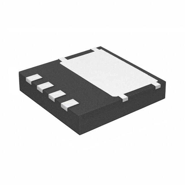
The Power88 package is an ultra−slim surface−mount package
(1 mm high) with a low profile and small footprint (8 x 8 mm2).
SUPERFET III MOSFET in a Power88 package offers excellent
switching performance due to lower parasitic source inductance and
separated power and drive sources. Power88 offers Moisture
Sensitivity Level 1 (MSL 1).
RDS(ON) MAX
ID MAX
650 V
64 mW @ 10 V
40 A
D
G
S1 S2
S1: Driver Source
S2: Power Source
POWER MOSFET
Features
•
•
•
•
•
•
VDSS
700 V @ TJ = 150°C
Typ. RDS(on) = 52 mW
Ultra Low Gate Charge (Typ. Qg = 82 nC)
Low Effective Output Capacitance (Typ. Coss(eff.) = 750 pF)
100% Avalanche Tested
These Devices are Pb−Free and are RoHS Compliant
Applications
• Telecom / Server Power Supplies
• Industrial Power Supplies
• UPS / Solar
G
S1
S2
S2
TDFN4 8X8 2P
CASE 520AB
MARKING DIAGRAM
NTMT064
N65S3H
AWLYWW
NTMT064N65S3H
A
WL
Y
WW
= Specific Device Code
= Assembly Location
= Wafer Lot
= Year
= Work Week
ORDERING INFORMATION
See detailed ordering and shipping information on page 2 of
this data sheet.
© Semiconductor Components Industries, LLC, 2018
March, 2021 − Rev. 1
1
Publication Order Number:
NTMT064N65S3H/D
�NTMT064N65S3H
ABSOLUTE MAXIMUM RATINGS (TC = 25°C, Unless otherwise noted)
Symbol
Parameter
VDSS
Drain to Source Voltage
VGSS
Gate to Source Voltage
ID
Drain Current
Value
Unit
650
V
− DC
±30
V
− AC (f > 1 Hz)
±30
− Continuous (TC = 25°C)
40
− Continuous (TC = 100°C)
25
IDM
Drain Current
112
A
EAS
Single Pulsed Avalanche Energy (Note 2)
422
mJ
IAS
Avalanche Current (Note 2)
6.5
A
EAR
Repetitive Avalanche Energy (Note 1)
2.60
mJ
dv/dt
MOSFET dv/dt
120
V/ns
Peak Diode Recovery dv/dt (Note 3)
20
PD
TJ, TSTG
TL
− Pulsed (Note 1)
A
Power Dissipation
(TC = 25°C)
260
W
− Derate Above 25°C
2.08
W/°C
−55 to +150
°C
260
°C
Operating and Storage Temperature Range
Maximum Lead Temperature for Soldering, 1/8″ from Case for 5 seconds
Stresses exceeding those listed in the Maximum Ratings table may damage the device. If any of these limits are exceeded, device functionality
should not be assumed, damage may occur and reliability may be affected.
1. Repetitive rating: pulse−width limited by maximum junction temperature.
2. IAS = 6.5 A, RG = 25 W, starting TJ = 25°C.
3. ISD ≤ 20 A, di/dt ≤ 200 A/ms, VDD ≤ 400 V, starting TJ = 25°C.
THERMAL CHARACTERISTICS
Symbol
Parameter
Value
Unit
RqJC
Thermal Resistance, Junction to Case, Max.
0.48
_C/W
RqJA
Thermal Resistance, Junction to Ambient, Max. (Note 4)
45
4. Device on 1 in2 pad 2 oz copper pad on 1.5 x 1.5 in. board of FR−4 material.
PACKAGE MARKING AND ORDERING INFORMATION
Part Number
Top Marking
Package
Reel Size
Tape Width
Shipping Quantity†
NTMT064N65S3H
NTMT064N65S3H
TDFN4
13″
13.3 mm
3000 Units / Tape & Reel
†For information on tape and reel specifications, including part orientation and tape sizes, please refer to our Tape and Reel Packaging
Specifications Brochure, BRD8011/D.
www.onsemi.com
2
�NTMT064N65S3H
ELECTRICAL CHARACTERISTICS (TC = 25°C unless otherwise noted)
Parameter
Symbol
Test Conditions
Min.
Typ.
Max.
Unit
VGS = 0 V, ID = 1 mA, TJ = 25_C
650
V
VGS = 0 V, ID = 1 mA, TJ = 150_C
700
V
OFF CHARACTERISTICS
BVDSS
Drain to Source Breakdown Voltage
DBVDSS/DTJ
Breakdown Voltage Temperature
Coefficient
ID = 10 mA, Referenced to 25_C
IDSS
Zero Gate Voltage Drain Current
VDS = 650 V, VGS = 0 V
IGSS
Gate to Body Leakage Current
0.63
V/_C
10
mA
±100
nA
4.0
V
64
mW
3.2
VDS = 520 V, TC = 125_C
VGS = ±30 V, VDS = 0 V
ON CHARACTERISTICS
VGS(th)
Gate Threshold Voltage
RDS(on)
Static Drain to Source On Resistance
VGS = 10 V, ID = 20 A
52
Forward Transconductance
VDS = 20 V, ID = 20 A
44
S
3745
pF
58
pF
gFS
VGS = VDS, ID = 3.9 mA
2.4
DYNAMIC CHARACTERISTICS
Ciss
Input Capacitance
Coss
Output Capacitance
VDS = 400 V, VGS = 0 V, f = 250 kHz
Coss(eff.)
Effective Output Capacitance
VDS = 0 V to 400 V, VGS = 0 V
750
pF
Coss(er.)
Energy Related Output Capacitance
VDS = 0 V to 400 V, VGS = 0 V
100
pF
Qg(tot)
Total Gate Charge at 10 V
Qgs
Gate to Source Gate Charge
Qgd
Gate to Drain “Miller” Charge
ESR
Equivalent Series Resistance
82
nC
VDS = 400 V, ID = 20 A, VGS = 10 V
(Note 5)
20
nC
23
nC
f = 1 MHz
0.7
W
29
ns
16
ns
85
ns
3.1
ns
SWITCHING CHARACTERISTICS
td(on)
Turn-On Delay Time
tr
Turn-On Rise Time
td(off)
Turn-Off Delay Time
tf
VDD = 400 V, ID = 20 A,
VGS = 10 V, Rg = 4.7 W
(Note 5)
Turn-Off Fall Time
SOURCE-DRAIN DIODE CHARACTERISTICS
Maximum Continuous Source to Drain Diode Forward Current
40
A
ISM
Maximum Pulsed Source to Drain Diode Forward Current
112
A
VSD
Source to Drain Diode Forward
Voltage
1.2
V
IS
trr
Reverse Recovery Time
Qrr
Reverse Recovery Charge
VGS = 0 V, ISD = 20 A
VDD = 400 V, ISD = 20 A,
dIF/dt = 100 A/ms
367
ns
6.3
mC
Product parametric performance is indicated in the Electrical Characteristics for the listed test conditions, unless otherwise noted. Product
performance may not be indicated by the Electrical Characteristics if operated under different conditions.
5. Essentially independent of operating temperature typical characteristics.
www.onsemi.com
3
�NTMT064N65S3H
TYPICAL CHARACTERISTICS
200
VGS = 4 V
100 4.5 V
5V
5.5 V
6V
6.5 V
7V
8V
10
10 V
RDS(on), DRAIN−TO−SOURCE ON−RESISTANCE (W)
ID, DRAIN CURRENT (A)
2
TJ = 150°C
10
TJ = 25°C
250 ms Pulse Test
TC = 25°C
1
0.2
1
20
TJ = −55°C
2.0
3.0
6.0
5.0
4.0
VDS, DRAIN−TO−SOURCE VOLTAGE (V)
VGS, GATE−TO−SOURCE VOLTAGE (V)
Figure 1. On−Region Characteristics
Figure 2. Transfer Characteristics
7.0
0.10
TC = 25°C
0.09
VGS = 10 V
0.08
0.07
VGS = 20 V
0.06
0.05
0.04
0
20
40
60
80
100
VGS = 0 V
250 ms Pulse Test
10
1
TJ = 150°C
0.1
TJ = 25°C
0.01
0.001
TJ = −55°C
0
0.2
0.6
0.4
1.0
0.8
VSD, BODY DIODE FORWARD VOLTAGE (V)
Figure 3. On−Resistance Variation vs. Drain
Current and Gate Voltage
Figure 4. Body Diode Forward Voltage
Variation vs. Source Current and
Temperature
VGS, GATE−TO−SOURCE VOLTAGE (V)
10K
Ciss
1K
100
100
ID, DRAIN CURRENT (A)
100K
CAPACITANCE (pF)
VDS = 20 V
250 ms Pulse Test
100
IS, REVERSE DRAIN CURRENT (A)
ID, DRAIN CURRENT (A)
1000
Coss
f = 250 kHz
VGS = 0 V
10 Ciss = Cgs + Cgd (Cds = shorted)
Coss = Cds + Cgd
Crss = Cgd
1
0.1
1
10
Crss
100
10
ID = 20 A
VDS = 130 V
8
VDS = 400 V
6
4
2
0
0
18
36
54
72
VDS, DRAIN−TO−SOURCE VOLTAGE (V)
Qg, TOTAL GATE CHARGE (nC)
Figure 5. Capacitance Characteristics
Figure 6. Gate Charge Characteristics
www.onsemi.com
4
1.2
90
�NTMT064N65S3H
TYPICAL CHARACTERISTICS
3.0
VGS = 0 V
ID = 10 mA
RDS(on), [NORMALIZED] DRAIN−TO−
SOURCE ON−RESISTANCE
BVDSS, [NORMALIZED] DRAIN−TO−
SOURCE BREAKDOWN VOLTAGE
1.2
1.1
1.0
0.9
0.8
−75 −50 −25
0
25
50
75
100 125
0.5
0
−75 −50
50
75
100 125
ID, DRAIN CURRENT (A)
10 ms
TC = 25°C
Single Pulse
TJ = 150°C
1
30
25
20
15
10
5
10
1000
100
0
25
50
75
100
125
VDS, DRAIN−TO−SOURCE VOLTAGE (V)
TC, CASE TEMPERATURE (°C)
Figure 9. Maximum Safe Operating Area
Figure 10. Maximum Drain Current
vs. Case Temperature
15
10
5
130
150 175
35
20
EOSS (mJ)
25
40
1 ms
Operation in this
Area is Limited by
RDS(on)
0
0
45
DC
0
−25
Figure 8. On−Resistance Variation
vs. Temperature
10
0.01
1.0
Figure 7. Breakdown Voltage Variation
vs. Temperature
100 ms
0.1
1.5
TJ, JUNCTION TEMPERATURE (°C)
30 ms
1
2.0
TJ, JUNCTION TEMPERATURE (°C)
200
100
ID, DRAIN CURRENT (A)
150 175
VGS = 10 V
ID = 20 A
2.5
260
390
650
520
VDS, DRAIN−TO−SOURCE VOLTAGE (V)
Figure 11. EOSS vs. Drain−to−Source Voltage
www.onsemi.com
5
150
�NTMT064N65S3H
r(t) NORMALIZED EFFECTIVE TRANSIENT THERMAL RESISTANCE
TYPICAL CHARACTERISTICS
2
1
50% Duty Cycle
20%
0.1
10%
5%
2%
1%
0.01
Single Pulse
0.001
10−5
10−4
10−3
10−2
10−1
t, RECTANGULAR PULSE DURATIONTIME (s)
Figure 12. Transient Thermal Response Curve
www.onsemi.com
6
100
101
�NTMT064N65S3H
VGS
RL
Qg
VDS
VGS
Qgs
Qgd
DUT
IG = Const.
Charge
Figure 13. Gate Charge Test Circuit & Waveform
RL
VDS
VDS
90%
90%
90%
VDD
VGS
RG
VGS
DUT
VGS
10%
td(on)
10%
tr
td(off)
ton
tf
toff
Figure 14. Resistive Switching Test Circuit & Waveforms
L
E AS + 1 @ LI AS
2
VDS
BVDSS
ID
IAS
RG
VDD
DUT
VGS
2
ID(t)
VDD
VDS(t)
tp
tp
Figure 15. Unclamped Inductive Switching Test Circuit & Waveforms
www.onsemi.com
7
Time
�NTMT064N65S3H
+
DUT
VDS
−
ISD
L
Driver
RG
Same Type
as DUT
VGS
− dv/dt controlled by RG
− ISD controlled by pulse period
D+
VGS
(Driver)
VDD
Gate Pulse Width
Gate Pulse Period
10 V
IFM, Body Diode Forward Current
ISD
(DUT)
di/dt
IRM
Body Diode Reverse Current
Body Diode Recovery dv/dt
VDS
(DUT)
VDD
VSD
Body Diode
Forward Voltage Drop
Figure 16. Peak Diode Recovery dv/dt Test Circuit & Waveforms
SUPERFET is a registered trademark of Semiconductor Components Industries, LLC.
www.onsemi.com
8
�NTMT064N65S3H
PACKAGE DIMENSIONS
TDFN4 8x8, 2P
CASE 520AB
ISSUE O
www.onsemi.com
9
�NTMT064N65S3H
ON Semiconductor and
are trademarks of Semiconductor Components Industries, LLC dba ON Semiconductor or its subsidiaries in the United States and/or other countries.
ON Semiconductor owns the rights to a number of patents, trademarks, copyrights, trade secrets, and other intellectual property. A listing of ON Semiconductor’s product/patent
coverage may be accessed at www.onsemi.com/site/pdf/Patent−Marking.pdf. ON Semiconductor reserves the right to make changes without further notice to any products herein.
ON Semiconductor makes no warranty, representation or guarantee regarding the suitability of its products for any particular purpose, nor does ON Semiconductor assume any liability
arising out of the application or use of any product or circuit, and specifically disclaims any and all liability, including without limitation special, consequential or incidental damages.
Buyer is responsible for its products and applications using ON Semiconductor products, including compliance with all laws, regulations and safety requirements or standards,
regardless of any support or applications information provided by ON Semiconductor. “Typical” parameters which may be provided in ON Semiconductor data sheets and/or
specifications can and do vary in different applications and actual performance may vary over time. All operating parameters, including “Typicals” must be validated for each customer
application by customer’s technical experts. ON Semiconductor does not convey any license under its patent rights nor the rights of others. ON Semiconductor products are not
designed, intended, or authorized for use as a critical component in life support systems or any FDA Class 3 medical devices or medical devices with a same or similar classification
in a foreign jurisdiction or any devices intended for implantation in the human body. Should Buyer purchase or use ON Semiconductor products for any such unintended or unauthorized
application, Buyer shall indemnify and hold ON Semiconductor and its officers, employees, subsidiaries, affiliates, and distributors harmless against all claims, costs, damages, and
expenses, and reasonable attorney fees arising out of, directly or indirectly, any claim of personal injury or death associated with such unintended or unauthorized use, even if such
claim alleges that ON Semiconductor was negligent regarding the design or manufacture of the part. ON Semiconductor is an Equal Opportunity/Affirmative Action Employer. This
literature is subject to all applicable copyright laws and is not for resale in any manner.
PUBLICATION ORDERING INFORMATION
LITERATURE FULFILLMENT:
Email Requests to: orderlit@onsemi.com
ON Semiconductor Website: www.onsemi.com
◊
TECHNICAL SUPPORT
North American Technical Support:
Voice Mail: 1 800−282−9855 Toll Free USA/Canada
Phone: 011 421 33 790 2910
www.onsemi.com
10
Europe, Middle East and Africa Technical Support:
Phone: 00421 33 790 2910
For additional information, please contact your local Sales Representative
�