NTTD4401F
FETKYt Power MOSFET
and Schottky Diode
−20 V, −3.3 A P−Channel with 20 V,
1.0 A Schottky Diode, Micro8t Package
http://onsemi.com
The FETKY product family incorporates low RDS(on), true logic level
MOSFETs packaged with industry leading, low forward drop, low
leakage Schottky Barrier Diodes to offer high efficiency components in
a space saving configuration. Independent pinouts for TMOS and
Schottky die allow the flexibility to use a single component for
switching and rectification functions in a wide variety of applications.
MOSFET PRODUCT SUMMARY
V(BR)DSS
•
•
ID Max
70 mW @ −4.5 V
−3.3 A
100 mW @ −2.7 V
−2.7 A
−20 V
Features
• Low VF and Low Leakage Schottky Diode
• Lower Component Placement and Inventory Costs along with Board
RDS(on) Typ
SCHOTTKY DIODE SUMMARY
VR Max
IF Max
VF Max
20 V
2.0 A
600 mV @ IF = 2.0 A
Space Savings
Logic Level Gate Drive – Can be Driven by Logic ICs
Pb−Free Package is Available
A
S
Applications
•
•
•
•
Buck Converter
Synchronous Rectification
Low Voltage Motor Control
Load Management in Battery Packs, Chargers, Cell Phones, and
other Portable Products
G
C
D
P−Channel MOSFET
Schottky Diode
MOSFET MAXIMUM RATINGS (TA = 25°C unless otherwise noted)
Symbol
Rating
Value
Unit
Drain−to−Source Voltage
VDSS
−20
V
Gate−to−Source Voltage
VGS
$10
V
ID
−3.3
A
TA = 25°C
Continuous Drain
Current (Note 1)
Power Dissipation
(Note 1)
TA = 100°C
Steady
State
Continuous Drain
Current (Note 2)
Power Dissipation
(Note 2)
TA = 25°C
PD
1.42
W
TA = 25°C
ID
−2.4
A
W
IDM
−10
A
TJ, TSTG
−55 to
150
°C
Single Pulse Drain−to−Source Avalanche
Energy Starting TA = 25°C (t v 10 s)
EAS
150
mJ
Lead Temperature for Soldering Purposes
(1/8″ from case for 10 s)
TL
260
°C
Operating Junction and
Storage Temperature
Stresses exceeding Maximum Ratings may damage the device. Maximum
Ratings are stress ratings only. Functional operation above the Recommended
Operating Conditions is not implied. Extended exposure to stresses above the
Recommended Operating Conditions may affect device reliability.
1. Surface−mounted on FR4 board using 1 in sq pad size
(Cu area = 1.127 in sq [1 oz] including traces).
2. Surface−mounted on FR4 board using the minimum recommended pad size
(Cu area = 0.172 in sq).
© Semiconductor Components Industries, LLC, 2007
April, 2007 − Rev. 6
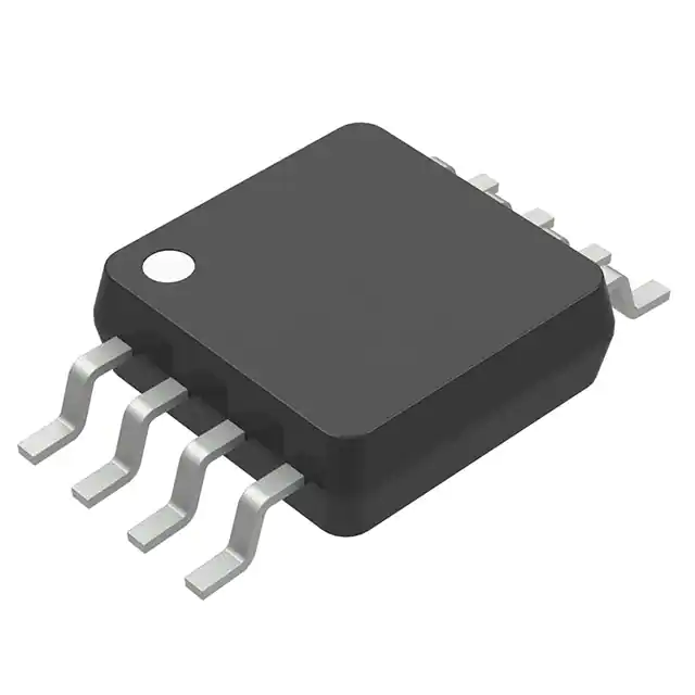
Micro8
CASE 846A
1
A AS G
0.78
t = 10 ms
WW
BG G
G
1
−1.5
PD
Pulsed Drain
Current
TA = 25°C
C CD D
8
8
−2.1
TA = 100°C
Steady
State
MARKING DIAGRAM &
PIN ASSIGNMENT
1
BG
= Specific Device Code
WW
= Work Week
G
= Pb−Free Package
(Note: Microdot may be in either location)
ORDERING INFORMATION
Device
NTTD4401FR2
NTTD4401FR2G
Package
Shipping†
Micro8
4000/Tape & Reel
Micro8
(Pb−Free)
4000/Tape & Reel
†For information on tape and reel specifications,
including part orientation and tape sizes, please
refer to our Tape and Reel Packaging Specification
Brochure, BRD8011/D.
Publication Order Number:
NTTD4401F/D
�NTTD4401F
SCHOTTKY DIODE MAXIMUM RATINGS (TA = 25°C unless otherwise noted)
Rating
Symbol
Value
Unit
V
20
V
Peak Repetitive Reverse Voltage
Average Forward Current (Rated VR, TA = 100°C)
IO
1.0
A
Peak Repetitive Forward Current (Note 3)
IFRM
2.0
A
Non−Repetitive Peak Surge Current (Note 4)
IFSM
20
A
THERMAL RESISTANCE RATINGS
FET
Rating
Schottky
Max
Symbol
Unit
Junction−to−Ambient – Steady State (Note 5)
RqJA
88
135
°C/W
Junction−to−Ambient – Steady State (Note 6)
RqJA
160
250
°C/W
MOSFET ELECTRICAL CHARACTERISTICS (TA = 25°C unless otherwise noted)
Characteristic
Symbol
Test Condition
Min
Typ
Max
Unit
V(BR)DSS
VGS = 0 V
−20
−
−
V
IDSS
VGS = 0 V, VDS = −16 V
−
−
−1.0
mA
VGS = 0 V, TJ = 125°C, VDS = −16 V
−
−
−25
IGSS
VDS = 0 V, VGS = ±10 V
−
−
±100
OFF CHARACTERISTICS
Drain−to−Source Breakdown Voltage
Zero Gate Voltage Drain Current (Note 7)
Gate−to−Source Leakage Current
nA
ON CHARACTERISTICS
Gate Threshold Voltage
Negative Threshold
Temperature Coefficient
Drain−to−Source On Resistance
VGS(TH)
VGS = VDS, ID = −250 mA
−0.5
−
−1.5
V
VGS(TH)/TJ
−
−
2.5
−
mV/°C
RDS(on)
VGS = −4.5 V, ID = −3.3 A
−
70
90
mW
VGS = −2.5 V, ID = −1.2 A
−
100
150
VDS = −10 V, ID = −2.7 A
−
4.2
−
S
−
550
750
pF
−
200
300
−
50
175
Forward Transconductance
gFS
CHARGES, CAPACITANCES AND GATE RESISTANCE
Input Capacitance
CISS
Output Capacitance
COSS
Reverse Transfer Capacitance
CRSS
Total Gate Charge
VGS = 0 V, f = 1.0 MHz,
VDS = −16 V
QG(TOT)
nC
−
10
18
−
1.5
3.0
QGD
−
5.0
10
td(ON)
−
11
20
−
35
65
−
33
60
−
29
55
−
−0.88
−1.0
V
−
37
50
ns
−
16
−
−
21
−
−
0.025
0.05
Gate−to−Source Gate Charge
QGS
Gate−to−Drain “Miller’’ Charge
VGS = −4.5 V, VDS = −16 V,
ID = −3.3 A
SWITCHING CHARACTERISTICS
Turn−On Delay Time
Rise Time
Turn−Off Delay Time
tr
td(OFF)
Fall Time
VGS = −4.5 V, VDD = −10 V,
ID = −3.3 A, RG = 6.0 W
tf
ns
DRAIN−SOURCE DIODE CHARACTERISTICS
Forward Diode Voltage
VSD
Reverse Recovery Time
tRR
Charge Time
ta
Discharge Time
tb
Reverse Recovery Charge
3.
4.
5.
6.
7.
VGS = 0 V, IS = −2.0 A
VGS = 0 V, dIS/dt = 100 A/ms,
IS = −3.3 A
QRR
−
Rated VR, square wave, 20 kHz, TA = 105°C.
Surge applied at rated load conditions, half−wave, single phase, 60 Hz.
Surface−mounted on FR4 board using 1 inch sq pad size (Cu area = 1.127 in sq [1 oz] including traces).
Surface−mounted on FR4 board using the minimum recommended pad size (Cu area = 0.172 in sq).
Body diode leakage current.
http://onsemi.com
2
nC
�NTTD4401F
SCHOTTKY DIODE ELECTRICAL CHARACTERISTICS (TJ = 25°C unless otherwise noted)
Symbol
Test Condition
Min
Typ
Reverse Breakdown Voltage
BV
IR = 1.0 mA
Reverse Leakage Current
IR
Characteristic
Forward Voltage
VF
VR = 20 V
IF = 1.0 A
IF = 2.0 A
Voltage Rate of Change
dV/dt
VR = 20 V
http://onsemi.com
3
Max
Unit
20
−
−
V
TA = 25°C
−
−
0.05
mA
TA = 125°C
−
−
10
TA = 25°C
−
−
0.5
TA = 125°C
−
−
0.39
TA = 25°C
−
−
0.6
TA = 125°C
−
−
0.53
−
10,000
−
V
V/ms
�NTTD4401F
TYPICAL ELECTRICAL CHARACTERISTICS
4
5
VGS = −10 V
VGS = −4.5 V
VGS = −2.5 V
3
TJ = 25°C
−ID, DRAIN CURRENT (AMPS)
−ID, DRAIN CURRENT (AMPS)
VGS = −2.1 V
VGS = −1.9 V
2
VGS = −1.7 V
1
VGS = −1.5 V
4
3
2
TJ = 25°C
1
TJ = 100°C
0
2
4
6
8
10
3
2.5
Figure 1. On−Region Characteristics
Figure 2. Transfer Characteristics
RDS(on), DRAIN−TO−SOURCE RESISTANCE (W)
−VGS, GATE−TO−SOURCE VOLTAGE (VOLTS)
0.15
0.1
0.05
0
2
4
6
8
−VGS, GATE−TO−SOURCE VOLTAGE (VOLTS)
0.12
TJ = 25°C
0.1
VGS = −2.7 V
0.08
VGS = −4.5 V
0.06
0.04
1
1.5
2
2.5
3
3.5
4
4.5
−ID, DRAIN CURRENT (AMPS)
Figure 3. On−Resistance vs. Gate−to−Source
Voltage
Figure 4. On−Resistance vs. Drain Current and
Gate Voltage
1.6
1000
VGS = 0 V
ID = −3.3 A
VGS = −4.5 V
TJ = 125°C
−IDSS, LEAKAGE (nA)
100
1.2
1
0.8
0.6
−50
2
−VDS, DRAIN−TO−SOURCE VOLTAGE (VOLTS)
TJ = 25°C
1.4
1.5
1
0.2
RDS(on), DRAIN−TO−SOURCE
RESISTANCE (NORMALIZED)
TJ = 55°C
0
0
RDS(on), DRAIN−TO−SOURCE RESISTANCE (W)
VDS > = −10 V
TJ = 100°C
10
TJ = 25°C
1
0.1
0.01
−25
50
100
125
0
25
75
TJ, JUNCTION TEMPERATURE (°C)
150
0
Figure 5. On−Resistance Variation with
Temperature
4
8
12
16
−VDS, DRAIN−TO−SOURCE VOLTAGE (VOLTS)
Figure 6. Drain−to−Source Leakage Current
vs. Voltage
http://onsemi.com
4
20
�NTTD4401F
C, CAPACITANCE (pF)
VDS = 0 V
1200
VGS = 0 V
Ciss
TJ = 25°C
900
Crss
Ciss
600
300
Coss
Crss
0
10
5
0
−VGS −VDS
5
10
15
20
5
20
18
QT
16
4
14
3
10
Q2
8
2
6
1
ID = −3.3 A
TJ = 25°C
VDS
2
0
0
2
4
6
8
12
10
Figure 8. Gate−to−Source and
Drain−to−Source Voltage vs. Total Charge
1000
100
td (off)
VDD = −10 V
ID = −1.2 A
VGS = −2.7 V
t, TIME (ns)
tr
tr
tf
td (on)
10
tf
td (off)
VDD = −10 V
ID = −3.3 A
VGS = −4.5 V
td (on)
1.0
10
10
1.0
14
Qg, TOTAL GATE CHARGE (nC)
Figure 7. Capacitance Variation
100
4
0
GATE−TO−SOURCE OR DRAIN−TO−SOURCE VOLTAGE (VOLTS)
t, TIME (ns)
12
VGS
Q1
100
RG, GATE RESISTANCE (W)
1.0
10
RG, GATE RESISTANCE (W)
Figure 9. Resistive Switching Time Variation
vs. Gate Resistance
Figure 10. Resistive Switching Time Variation
vs. Gate Resistance
100
−IS, SOURCE CURRENT (AMPS)
2
1.6
VGS = 0 V
TJ = 25°C
di/dt
IS
trr
1.2
ta
tb
TIME
0.8
0.25 IS
tp
IS
0.4
0
0.4
0.5
0.6
0.7
−VDS, DRAIN−TO−SOURCE VOLTAGE (VOLTS)
1500
−VGS, GATE−TO−SOURCE VOLTAGE (VOLTS)
TYPICAL ELECTRICAL CHARACTERISTICS
0.8
0.9
1
Figure 12. Diode Reverse Recovery Waveform
−VSD, SOURCE−TO−DRAIN VOLTAGE (VOLTS)
Figure 11. Diode Forward Voltage
vs. Current
http://onsemi.com
5
�NTTD4401F
Rthja(t), EFFECTIVE TRANSIENT THERMAL RESPONSE
1
D = 0.5
0.2
0.1
Normalized to R∅ja at Steady State (1 inch pad)
0.1
0.0125 W 0.0563 W
0.110 W
0.273 W
0.113 W
0.436 W
2.93 F
152 F
261 F
0.05
0.02
0.01
0.021 F
0.137 F
1.15 F
Single Pulse
0.01
1E−03
1E−02
1E−01
1E+00
1E+03
1E+02
1E+03
t, TIME (s)
Figure 13. FET Thermal Response
10
IF, INSTANTANEOUS FORWARD CURRENT (AMPS)
IF, INSTANTANEOUS FORWARD CURRENT (AMPS)
TYPICAL SCHOTTKY ELECTRICAL CHARACTERISTICS
TJ = 125°C
1.0
85°C
25°C
−�40 °C
0.1
0.1
0.2
0.3
0.4
0.5
0.6
0.7
0.8
0.9
1.0
10
TJ = 125°C
85°C
1.0
25°C
0.1
0
VF, INSTANTANEOUS FORWARD VOLTAGE (VOLTS)
0.2
0.4
0.6
0.8
1.0
1.2
VF, MAXIMUM INSTANTANEOUS FORWARD VOLTAGE (VOLTS)
Figure 14. Typical Forward Voltage
Figure 15. Maximum Forward Voltage
http://onsemi.com
6
1.4
�NTTD4401F
TYPICAL SCHOTTKY ELECTRICAL CHARACTERISTICS
IR, MAXIMUM REVERSE CURRENT (AMPS)
IR, REVERSE CURRENT (AMPS)
1E−2
TJ = 125°C
1E−3
85°C
1E−4
1E−5
25°C
1E−6
1E−7
1E−1
TJ = 125°C
1E−2
1E−3
1E−4
25°C
1E−5
1E−6
0
5.0
10
15
20
5.0
0
VR, REVERSE VOLTAGE (VOLTS)
IO , AVERAGE FORWARD CURRENT (AMPS)
C, CAPACITANCE (pF)
TYPICAL CAPACITANCE AT 0 V = 170 pF
100
10
15
10
20
1.6
dc
1.2
SQUARE WAVE
1.0
Ipk/Io = p
0.8
Ipk/Io = 5.0
0.6
Ipk/Io = 10
0.4
Ipk/Io = 20
0.2
0
0
20
40
60
0.6
dc
SQUARE
WAVE
Ipk/Io = p
Ipk/Io = 5.0
Ipk/Io = 10
0.3
Ipk/Io = 20
0.2
0.1
0
0
100
120
Figure 19. Current Derating
0.7
0.4
80
TA, AMBIENT TEMPERATURE (°C)
Figure 18. Typical Capacitance
PFO , AVERAGE POWER DISSIPATION (WATTS)
FREQ = 20 kHz
1.4
VR, REVERSE VOLTAGE (VOLTS)
0.5
20
Figure 17. Maximum Reverse Current
1000
5.0
15
VR, REVERSE VOLTAGE (VOLTS)
Figure 16. Typical Reverse Current
0
10
0.5
1.0
1.5
IO, AVERAGE FORWARD CURRENT (AMPS)
Figure 20. Forward Power Dissipation
FETKY and Micro8 are registered trademarks of International Rectifier Corporation.
http://onsemi.com
7
2.0
140
160
�MECHANICAL CASE OUTLINE
PACKAGE DIMENSIONS
Micro8
CASE 846A−02
ISSUE K
DATE 16 JUL 2020
SCALE 2:1
GENERIC
MARKING DIAGRAM*
8
XXXX
AYWG
G
1
XXXX
A
Y
W
G
= Specific Device Code
= Assembly Location
= Year
= Work Week
= Pb−Free Package
(Note: Microdot may be in either location)
*This information is generic. Please refer to
device data sheet for actual part marking.
Pb−Free indicator, “G” or microdot “G”, may
or may not be present. Some products may
not follow the Generic Marking.
DOCUMENT NUMBER:
DESCRIPTION:
98ASB14087C
MICRO8
STYLE 1:
PIN 1.
2.
3.
4.
5.
6.
7.
8.
SOURCE
SOURCE
SOURCE
GATE
DRAIN
DRAIN
DRAIN
DRAIN
STYLE 2:
PIN 1.
2.
3.
4.
5.
6.
7.
8.
SOURCE 1
GATE 1
SOURCE 2
GATE 2
DRAIN 2
DRAIN 2
DRAIN 1
DRAIN 1
STYLE 3:
PIN 1.
2.
3.
4.
5.
6.
7.
8.
N-SOURCE
N-GATE
P-SOURCE
P-GATE
P-DRAIN
P-DRAIN
N-DRAIN
N-DRAIN
Electronic versions are uncontrolled except when accessed directly from the Document Repository.
Printed versions are uncontrolled except when stamped “CONTROLLED COPY” in red.
PAGE 1 OF 1
ON Semiconductor and
are trademarks of Semiconductor Components Industries, LLC dba ON Semiconductor or its subsidiaries in the United States and/or other countries.
ON Semiconductor reserves the right to make changes without further notice to any products herein. ON Semiconductor makes no warranty, representation or guarantee regarding
the suitability of its products for any particular purpose, nor does ON Semiconductor assume any liability arising out of the application or use of any product or circuit, and specifically
disclaims any and all liability, including without limitation special, consequential or incidental damages. ON Semiconductor does not convey any license under its patent rights nor the
rights of others.
© Semiconductor Components Industries, LLC, 2019
www.onsemi.com
�onsemi,
, and other names, marks, and brands are registered and/or common law trademarks of Semiconductor Components Industries, LLC dba “onsemi” or its affiliates
and/or subsidiaries in the United States and/or other countries. onsemi owns the rights to a number of patents, trademarks, copyrights, trade secrets, and other intellectual property.
A listing of onsemi’s product/patent coverage may be accessed at www.onsemi.com/site/pdf/Patent−Marking.pdf. onsemi reserves the right to make changes at any time to any
products or information herein, without notice. The information herein is provided “as−is” and onsemi makes no warranty, representation or guarantee regarding the accuracy of the
information, product features, availability, functionality, or suitability of its products for any particular purpose, nor does onsemi assume any liability arising out of the application or use
of any product or circuit, and specifically disclaims any and all liability, including without limitation special, consequential or incidental damages. Buyer is responsible for its products
and applications using onsemi products, including compliance with all laws, regulations and safety requirements or standards, regardless of any support or applications information
provided by onsemi. “Typical” parameters which may be provided in onsemi data sheets and/or specifications can and do vary in different applications and actual performance may
vary over time. All operating parameters, including “Typicals” must be validated for each customer application by customer’s technical experts. onsemi does not convey any license
under any of its intellectual property rights nor the rights of others. onsemi products are not designed, intended, or authorized for use as a critical component in life support systems
or any FDA Class 3 medical devices or medical devices with a same or similar classification in a foreign jurisdiction or any devices intended for implantation in the human body. Should
Buyer purchase or use onsemi products for any such unintended or unauthorized application, Buyer shall indemnify and hold onsemi and its officers, employees, subsidiaries, affiliates,
and distributors harmless against all claims, costs, damages, and expenses, and reasonable attorney fees arising out of, directly or indirectly, any claim of personal injury or death
associated with such unintended or unauthorized use, even if such claim alleges that onsemi was negligent regarding the design or manufacture of the part. onsemi is an Equal
Opportunity/Affirmative Action Employer. This literature is subject to all applicable copyright laws and is not for resale in any manner.
PUBLICATION ORDERING INFORMATION
LITERATURE FULFILLMENT:
Email Requests to: orderlit@onsemi.com
onsemi Website: www.onsemi.com
◊
TECHNICAL SUPPORT
North American Technical Support:
Voice Mail: 1 800−282−9855 Toll Free USA/Canada
Phone: 011 421 33 790 2910
Europe, Middle East and Africa Technical Support:
Phone: 00421 33 790 2910
For additional information, please contact your local Sales Representative
�