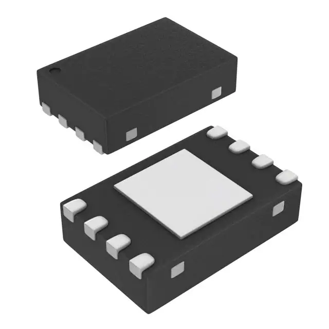
NUC2401MN Integrated Common Mode Choke with Integrated ESD Protection
Description
The NUC2401MN is an Integrated Common Mode Filter for the elimination of common mode noise in high speed data line applications such as IEEE1394, USB2.0 and other LVDS type applications. ESD protection is integrated into the Common mode filter for superior protection and significant part count reduction.
Features
http://onsemi.com SIMPLIFIED SCHEMATIC
VCC 6
• • • • • • •
Common mode EMI Filtering and ESD Protection Integration of 5 Discrete components ±12 kV ESD Protection per IEC61000−4−2 (Contact Discharge) DFN: 2.0 x 2.2 mm Package Moisture Sensitivity Level 1 ESD Rating: Machine Model (MM) = 1.6 kV; Human Body Model (HBM) = 16 kV This is a Pb−Free Device
I/O 1, 9 I/O 2, 10
I/O 8, 12 I/O 7, 11
MARKING DIAGRAM
8 1 DFN8 CASE 506BL 1 C2 MG G
Benefits
• Reduces EMI/RFI Emissions on a Data Line • Integrated Solution offers Cost and Space Savings • Reduces Parasitic Inductances Which Offer a More “Ideal” Common • • • • • • •
Mode Filtering Integrated Solution Improves System Reliability High Speed Differential Data Lines USB2.0 IEEE1394 LVDS MIPI MDDI
C2 = Specific Device Code M = Date Code G = Pb−Free Device (Note: Microdot may be in either location)
Applications
D− D+ GND GND
PIN CONNECTIONS*
1 2 3 4 N/C 9 10 N/C N/C 12 11 N/C 8 7 6 5 D− D+ VCC GND
GND (Top View)
*NOTE: Pins 1 and 9, Pins 2 and 10, Pins 7 and 11, Pins 8 and 12 are internally connected in pairs. It is recommended not to solder to Pins 9, 10, 11, 12.
ORDERING INFORMATION
Device NUC2401MNTAG Package DFN8 (Pb−Free) Shipping† 3000/Tape & Reel
†For information on tape and reel specifications, including part orientation and tape sizes, please refer to our Tape and Reel Packaging Specification Brochure, BRD8011/D.
© Semiconductor Components Industries, LLC, 2010
January, 2010 − Rev. 2
1
Publication Order Number: NUC2401MN/D
�NUC2401MN
MAXIMUM RATINGS (TA = 25°C unless otherwise stated)
Parameter ESD Discharge IEC61000−4−2 Operating Temperature Range Storage Temperature Range Maximum Lead Temperature for Soldering Purposes (1/8” from Case for 10 Seconds) DC Current per Line Contact Discharge Symbol VPP TOP TSTG TL ILINE Value ±12 −40 to 85 −55 to 125 260 100 Units kV °C °C °C mA
Stresses exceeding Maximum Ratings may damage the device. Maximum Ratings are stress ratings only. Functional operation above the Recommended Operating Conditions is not implied. Extended exposure to stresses above the Recommended Operating Conditions may affect device reliability.
ELECTRICAL CHARACTERISTICS (TA = 25°C unless otherwise specified)
Parameter Maximum Reverse Working Voltage Breakdown Voltage Leakage Current Maximum Peak Pulse Current Clamping Voltage Resistance Pin 1 to Pin 8 Resistance Pin 2 to Pin 7 Capacitance (Note 1) Capacitance (Note 2) Common Mode Cut−Off Frequency (Note 3) Common Mode Impedance Symbol VRWM VBR IR IPP VC RA RB CLINE 1 CLINE 2 f3dB ZC (Above this Frequency, Appreciable Common Mode Attenuation Occurs) @ 100 MHz IR = 1 mA VRWM = 5.5 V 8x20 ms Waveform IPP = 5 A 2.2 2.2 0.8 0.8 40 90 6.0 7.6 Test Conditions Min Typ Max 5.0 8.6 2.0 12 10 5.0 5.0 1.0 1.0 Unit V V mA A V W W pF pF MHz W
1. Measured at 25°C, VR = 0 V, f = 1 MHz, Pins 1 or 4 to GND. 2. Measured at 25°C, VR = 0 V, f = 1 MHz, Pins 8 or 5 to GND. 3. 50 W source and 50 W load termination.
10000
0 −5 Differential Mode
1000
IMPEDANCE (W) Common Mode
INSERTION LOSS (dB)
−10 −15 −20 −25 −30 Common Mode
100
10
Differential Mode
1 1
10
100
FREQUENCY (MHz)
1000
10000
−35
1
10
100 FREQUENCY (MHz)
1000
10000
Figure 1. Impedance Characteristics vs. Frequency
Figure 2. Insertion Loss Characteristics vs. Frequency
http://onsemi.com
2
�NUC2401MN
I/O 1 I/O 2
I/O 8 I/O 7
NUC2401MN 2 1 4 3
Network Analyzer
Normal (Differential) Mode
Figure 3. Normal (Differential) Mode Test Configuration
I/O 1 I/O 2 Differential Signal Driver and Transmission Line
I/O 8 I/O 7 Differential Signal Buffer and Transmission Line
NUC2401MN
Figure 4. Application Circuit
http://onsemi.com
3
�NUC2401MN
PACKAGE DIMENSIONS
DFN8, 2.2x2, 0.5P CASE 506BL−01 ISSUE O
D A B
NOTES: 1. DIMENSIONING AND TOLERANCING PER ASME Y14.5M, 1994. 2. CONTROLLING DIMENSION: MILLIMETERS. 3. DIMENSION b APPLIES TO PLATED TERMINAL AND IS MEASURED BETWEEN 0.15 AND 0.30 mm FROM TERMINAL. 4. COPLANARITY APPLIES TO THE EXPOSED PAD AS WELL AS THE TERMINALS. 5. EXPOSED ENDS OF THE TERMINALS ARE ELECTRICALLY ACTIVE. DIM A A1 A3 b D D2 E E2 e K L L1 MILLIMETERS MIN MAX 0.85 0.95 0.00 0.05 0.20 REF 0.15 0.25 2.20 BSC 0.34 0.54 2.00 BSC 0.60 0.80 0.50 BSC 0.20 −−− 0.30 0.50 −−− 0.15
2X
0.10 C
2X
0.10 C 0.10 C
9X
0.08 C
NOTE 4
A1 A3 SIDE VIEW
C
SEATING PLANE
OPTIONAL CONSTRUCTION
0.10 C A B
DETAIL A
L
D2
1 4
E2
L1 0.10 C A B DETAIL A
OPTIONAL CONSTRUCTIONS
K e
8
5
8X
b 0.10 C A B 0.05 C
NOTE 3
e/2 BOTTOM VIEW (0.28) (0.825)
(0.20)
1
(0.50) (0.25) AUXILIARY BOTTOM VIEW
(FOR REFERENCE ONLY) 4X
ON Semiconductor and are registered trademarks of Semiconductor Components Industries, LLC (SCILLC). SCILLC reserves the right to make changes without further notice to any products herein. SCILLC makes no warranty, representation or guarantee regarding the suitability of its products for any particular purpose, nor does SCILLC assume any liability arising out of the application or use of any product or circuit, and specifically disclaims any and all liability, including without limitation special, consequential or incidental damages. “Typical” parameters which may be provided in SCILLC data sheets and/or specifications can and do vary in different applications and actual performance may vary over time. All operating parameters, including “Typicals” must be validated for each customer application by customer’s technical experts. SCILLC does not convey any license under its patent rights nor the rights of others. SCILLC products are not designed, intended, or authorized for use as components in systems intended for surgical implant into the body, or other applications intended to support or sustain life, or for any other application in which the failure of the SCILLC product could create a situation where personal injury or death may occur. Should Buyer purchase or use SCILLC products for any such unintended or unauthorized application, Buyer shall indemnify and hold SCILLC and its officers, employees, subsidiaries, affiliates, and distributors harmless against all claims, costs, damages, and expenses, and reasonable attorney fees arising out of, directly or indirectly, any claim of personal injury or death associated with such unintended or unauthorized use, even if such claim alleges that SCILLC was negligent regarding the design or manufacture of the part. SCILLC is an Equal Opportunity/Affirmative Action Employer. This literature is subject to all applicable copyright laws and is not for resale in any manner.
PUBLICATION ORDERING INFORMATION
LITERATURE FULFILLMENT: Literature Distribution Center for ON Semiconductor P.O. Box 5163, Denver, Colorado 80217 USA Phone : 303−675−2175 or 800−344−3860 Toll Free USA/Canada Fax: 303−675−2176 or 800−344−3867 Toll Free USA/Canada Email: orderlit@onsemi.com N. American Technical Support: 800−282−9855 Toll Free USA/Canada Europe, Middle East and Africa Technical Support: Phone: 421 33 790 2910 Japan Customer Focus Center Phone: 81−3−5773−3850 ON Semiconductor Website: www.onsemi.com Order Literature: http://www.onsemi.com/orderlit For additional information, please contact your local Sales Representative
http://onsemi.com
4
ÉÉÉ ÇÇÇ
DETAIL B
ÉÉÉ ÉÉÉ ÉÉÉ
PIN ONE REFERENCE
E
NOTE 5
END VIEW
TOP VIEW
DETAIL B
A
EXPOSED Cu
MOLD CMPD
L
SOLDERING FOOTPRINT*
8X
0.24
0.90 0.55
2.30
0.62
8X
0.80
PACKAGE OUTLINE
0.50 PITCH
DIMENSIONS: MILLIMETERS
*For additional information on our Pb−Free strategy and soldering details, please download the ON Semiconductor Soldering and Mounting Techniques Reference Manual, SOLDERRM/D.
NUC2401MN/D
�


 工商网监
湘ICP备2023018690号
工商网监
湘ICP备2023018690号
