DATA SHEET
www.onsemi.com
LED Shunt
NUD4700
Anode
The NUD4700 is an electronic shunt which provides a current bypass
in the case of a single LED going into open circuit. LEDs are by nature
quite fragile when subjected to transients and surge conditions. There
are also many cases where high reliability of the LED lighting must be
maintained such as headlights, lighthouses, bridges, aircraft, runways
and so forth. In these cases the low cost addition of the NUD4700 will
provide full assurance that an entire string of LEDs will not extinguish
should one LED fail. NUD4700 is also applicable to other loads where
circuit continuity is required. This device is designed to be used with
1 W LEDs (nominally 350 mA @ 3 V).
Cathode
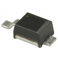
POWERMITE[
CASE 457
MARKING DIAGRAM
•
Cathode
M
= Date Code
MNH = Device Code
G
= Pb−Free Package
Features
•
•
•
•
•
•
M
MNHG
Anode
A Simple Two Terminal Device
Automatically Resets Itself if the LED Heals Itself or is Replaced
ON−State Voltage Typically 1 V
OFF−State Current less than 250 mA
Available with White Package
SZ Prefix (black package only) for Automotive and Other
Applications Requiring Unique Site and Control Change
Requirements; AEC−Q101 Qualified and PPAP Capable
These Devices are Pb−Free, Halogen Free/BFR Free and are RoHS
Compliant
Anode
Control
Circuit
Cathode
Typical Applications
•
•
•
•
•
PIN FUNCTION DESCRIPTION
LEDs where Preventive Maintenance is Non Practical
LED Headlights
LEDs with High Reliability Requirements
Crowbar Protection for Open Circuit Conditions
Overvoltage Protection for Sensitive Circuits
Pin
Description
Anode
Positive Input Voltage to the Device
Cathode
Negative Input Voltage to the Device
ORDERING INFORMATION
Package
Shipping†
POWERMITE
(Black)
3000/Tape &
Reel
SZNUD4700SNT1G POWERMITE
(Black)
3000/Tape &
Reel
Device
NUD4700SNT1G
†For information on tape and reel specifications,
including part orientation and tape sizes, please
refer to our Tape and Reel Packaging Specifications
Brochure, BRD8011/D.
© Semiconductor Components Industries, LLC, 2017
November, 2022 − Rev. 12
1
Publication Order Number:
NUD4700/D
�NUD4700
MAXIMUM RATINGS (Maximum ratings are those, that, if exceeded, may cause damage to the device. Electrical Characteristics are
not guaranteed over this range)
Rating
Symbol
Value
Unit
VDM
−0.3 to 10
V
Peak Repetitive Off State Voltage (Anode to Cathode)
Average On−State Current, (TA = 25°C),
(Note 1)
(Note 2)
IT(AVG)
Thermal Resistance, Junction−to−Air
(Note 1)
(Note 2)
QJA
Thermal Resistance, Junction−to−Lead
A
1.3
0.376
°C/W
80
277
35
QJL
°C/W
Power Dissipation (TA = 25°C)
(Note 1)
(Note 2)
PMAX
W
Operating Temperature Range
TJ
−40 to 150
°C
Non−Operating Temperature Range
TJ
150
°C
Lead Temperature, Soldering (10 Sec)
TL
260
°C
1.56
0.45
Stresses exceeding those listed in the Maximum Ratings table may damage the device. If any of these limits are exceeded, device functionality
should not be assumed, damage may occur and reliability may be affected.
1. Mounted onto a 1“ x 1” square copper pad.
Normally this device would be mounted on the same copper heat sink and adjacent to the LED. If the LED were to go open, then the NUD4700
shunt would now dissipate the power using the same copper heat sink. Since the NUD4700 has a voltage that is nominally 30% of the LED,
then the power dissipation would be easily handled by the same heat sink as the LED.
2. Device mounted on minimum copper pad.
ELECTRICAL CHARACTERISTICS (Unless otherwise noted: TA = 25°C)
Characteristics
Symbol
Min
Typ
Max
Unit
Off−State Current
(VAnode = 5 V)
ILEAK
−
100
250
mA
Breakdown Voltage
(IBR = 1 mA)
V(BR)
5.5
−
7.5
V
Holding Current
(VAnode = 10 V, Iinitial = 100 mA)
IH
−
6.0
12
mA
Latching Current
(VAnode = 10 V)
IL
−
35
70
mA
VT
−
−
−
1.0
1.0
1.0
1.2
−
−
V
dV/dt
250
−
−
V/ms
On−State Voltage
(IT = 0.350 A)
(IT = 0.750 A)
(IT = 1.0 A)
DYNAMIC CHARACTERISTICS
Critical Rate−of−Rise of Off State Voltage
(Vpk = Rated V(BR), TJ = 125°C, Exponential Method)
Product parametric performance is indicated in the Electrical Characteristics for the listed test conditions, unless otherwise noted. Product
performance may not be indicated by the Electrical Characteristics if operated under different conditions.
www.onsemi.com
2
�NUD4700
TYPICAL PERFORMANCE CURVES
(TA = 25°C UNLESS OTHERWISE NOTED)
6
35
IH, HOLDING CURRENT (mA)
IL, LATCHING CURRENT (mA)
40
30
25
20
15
10
5
0
−50
−25
0
25
50
75
100
125
3
2
1
0
25
50
75
100
125
150
TA, AMBIENT TEMPERATURE (°C)
TA, AMBIENT TEMPERATURE (°C)
Figure 2. Holding Current vs Temperature
IDSS, LEAKAGE CURRENT (mA)
450
90
80
70
60
50
0
1
2
3
4
400
350
300
250
200
150
100
50
0
−50
5
25
50
75
100
125
150
TA, AMBIENT TEMPERATURE (°C)
Figure 4. Leakage Current vs Temperature
1.2
1.1
IT @ 1.0 mA
1
IT @ 350 mA
0.6
0.4
IT @ 750 mA
0.2
−50
0
VOLTS (V)
1.2
0.8
−25
Figure 3. Capacitance vs Voltage
1.4
0
−25
Figure 1. Latching Current vs Temperature
VT, ON−STATE VOLTAGE (V)
Cd, CAPACITANCE (pF)
4
0
−50
150
100
VT, ON−STATE VOLTAGE (V)
5
−25
0
25
50
75
100
125
150
1
0.9
0.8
0.7
0.6
0.5
0.25
175
0.35
0.45
0.55
0.65
0.75
0.85
0.95
TEMPERATURE (°C)
IT, ON−STATE CURRNT (A)
Figure 5. On−State Voltage vs. Temperature
Figure 6. On−State Voltage vs. On−State
Current (IT) at 255C
www.onsemi.com
3
1.05
�NUD4700
TYPICAL APPLICATION CIRCUIT
Q1
AC/DC
Converter
NUD4001
R1
Current
Source
NUD4700
Control
Circuit
NUD4700
Control
Circuit
NUD4700
Control
Circuit
NUD4700
Control
Circuit
NUD4700
Control
Circuit
Figure 7. Typical Application Circuit
www.onsemi.com
4
�NUD4700
TYPICAL OPERATION WAVEFORMS
Switching event
LED being opened
LED Current
NUD4700 voltage
Off state
NUD4700 voltage
ON−state
NUD4700 switching
waveforms (Powermite)
Figure 8. NUD4700 Switching Waveforms
Switching event
LED being opened
Current overshoot
due to response time
of current source
LED Current
NUD4700 voltage
Off state
NUD4700 voltage
ON−state
NUD4700 switching
waveforms (zoom in)
Figure 9. Zoom in of Figure 8
POWERMITE is a registered trademarks of and used under a license from Microsemi Corporation.
www.onsemi.com
5
�MECHANICAL CASE OUTLINE
PACKAGE DIMENSIONS
POWERMITE
CASE 457
ISSUE G
DATE 12 JAN 2022
SCALE 4:1
GENERIC
MARKING DIAGRAMS*
1
M
XXXG
2
1
STYLE 1
1
M
XXXG
2
STYLE 2
M
XXXG
2
XXX = Specific Device Code
M = Date Code
G
= Pb−Free Package
STYLE 3
DOCUMENT NUMBER:
DESCRIPTION:
STYLE 1:
PIN 1. CATHODE
2. ANODE
98ASB14853C
POWERMITE
STYLE 2:
PIN 1. ANODE OR CATHODE
2. CATHODE OR ANODE
(BI−DIRECTIONAL)
STYLE 3:
PIN 1. ANODE
2. CATHODE
*This information is generic. Please refer to
device data sheet for actual part marking.
Pb−Free indicator, “G” or microdot “G”, may
or may not be present. Some products may
not follow the Generic Marking.
Electronic versions are uncontrolled except when accessed directly from the Document Repository.
Printed versions are uncontrolled except when stamped “CONTROLLED COPY” in red.
PAGE 1 OF 1
onsemi and
are trademarks of Semiconductor Components Industries, LLC dba onsemi or its subsidiaries in the United States and/or other countries. onsemi reserves
the right to make changes without further notice to any products herein. onsemi makes no warranty, representation or guarantee regarding the suitability of its products for any particular
purpose, nor does onsemi assume any liability arising out of the application or use of any product or circuit, and specifically disclaims any and all liability, including without limitation
special, consequential or incidental damages. onsemi does not convey any license under its patent rights nor the rights of others.
© Semiconductor Components Industries, LLC, 2019
www.onsemi.com
�onsemi,
, and other names, marks, and brands are registered and/or common law trademarks of Semiconductor Components Industries, LLC dba “onsemi” or its affiliates
and/or subsidiaries in the United States and/or other countries. onsemi owns the rights to a number of patents, trademarks, copyrights, trade secrets, and other intellectual property.
A listing of onsemi’s product/patent coverage may be accessed at www.onsemi.com/site/pdf/Patent−Marking.pdf. onsemi reserves the right to make changes at any time to any
products or information herein, without notice. The information herein is provided “as−is” and onsemi makes no warranty, representation or guarantee regarding the accuracy of the
information, product features, availability, functionality, or suitability of its products for any particular purpose, nor does onsemi assume any liability arising out of the application or use
of any product or circuit, and specifically disclaims any and all liability, including without limitation special, consequential or incidental damages. Buyer is responsible for its products
and applications using onsemi products, including compliance with all laws, regulations and safety requirements or standards, regardless of any support or applications information
provided by onsemi. “Typical” parameters which may be provided in onsemi data sheets and/or specifications can and do vary in different applications and actual performance may
vary over time. All operating parameters, including “Typicals” must be validated for each customer application by customer’s technical experts. onsemi does not convey any license
under any of its intellectual property rights nor the rights of others. onsemi products are not designed, intended, or authorized for use as a critical component in life support systems
or any FDA Class 3 medical devices or medical devices with a same or similar classification in a foreign jurisdiction or any devices intended for implantation in the human body. Should
Buyer purchase or use onsemi products for any such unintended or unauthorized application, Buyer shall indemnify and hold onsemi and its officers, employees, subsidiaries, affiliates,
and distributors harmless against all claims, costs, damages, and expenses, and reasonable attorney fees arising out of, directly or indirectly, any claim of personal injury or death
associated with such unintended or unauthorized use, even if such claim alleges that onsemi was negligent regarding the design or manufacture of the part. onsemi is an Equal
Opportunity/Affirmative Action Employer. This literature is subject to all applicable copyright laws and is not for resale in any manner.
PUBLICATION ORDERING INFORMATION
LITERATURE FULFILLMENT:
Email Requests to: orderlit@onsemi.com
onsemi Website: www.onsemi.com
◊
TECHNICAL SUPPORT
North American Technical Support:
Voice Mail: 1 800−282−9855 Toll Free USA/Canada
Phone: 011 421 33 790 2910
Europe, Middle East and Africa Technical Support:
Phone: 00421 33 790 2910
For additional information, please contact your local Sales Representative
�