ON Semiconductor
Is Now
To learn more about onsemi™, please visit our website at
www.onsemi.com
onsemi and and other names, marks, and brands are registered and/or common law trademarks of Semiconductor Components Industries, LLC dba “onsemi” or its affiliates and/or
subsidiaries in the United States and/or other countries. onsemi owns the rights to a number of patents, trademarks, copyrights, trade secrets, and other intellectual property. A listing of onsemi
product/patent coverage may be accessed at www.onsemi.com/site/pdf/Patent-Marking.pdf. onsemi reserves the right to make changes at any time to any products or information herein, without
notice. The information herein is provided “as-is” and onsemi makes no warranty, representation or guarantee regarding the accuracy of the information, product features, availability, functionality,
or suitability of its products for any particular purpose, nor does onsemi assume any liability arising out of the application or use of any product or circuit, and specifically disclaims any and all
liability, including without limitation special, consequential or incidental damages. Buyer is responsible for its products and applications using onsemi products, including compliance with all laws,
regulations and safety requirements or standards, regardless of any support or applications information provided by onsemi. “Typical” parameters which may be provided in onsemi data sheets and/
or specifications can and do vary in different applications and actual performance may vary over time. All operating parameters, including “Typicals” must be validated for each customer application
by customer’s technical experts. onsemi does not convey any license under any of its intellectual property rights nor the rights of others. onsemi products are not designed, intended, or authorized
for use as a critical component in life support systems or any FDA Class 3 medical devices or medical devices with a same or similar classification in a foreign jurisdiction or any devices intended for
implantation in the human body. Should Buyer purchase or use onsemi products for any such unintended or unauthorized application, Buyer shall indemnify and hold onsemi and its officers, employees,
subsidiaries, affiliates, and distributors harmless against all claims, costs, damages, and expenses, and reasonable attorney fees arising out of, directly or indirectly, any claim of personal injury or death
associated with such unintended or unauthorized use, even if such claim alleges that onsemi was negligent regarding the design or manufacture of the part. onsemi is an Equal Opportunity/Affirmative
Action Employer. This literature is subject to all applicable copyright laws and is not for resale in any manner. Other names and brands may be claimed as the property of others.
�NUF4105FC
4 Channel EMI Pi−Filter
Array with ESD Protection
+4 ESD Diodes
This device is a 4 channel EMI filter array for data lines. Greater
than −40 dB attenuation is obtained at frequencies from 800 MHz to
2.2 GHz. It also offers ESD protection − clamping transients from
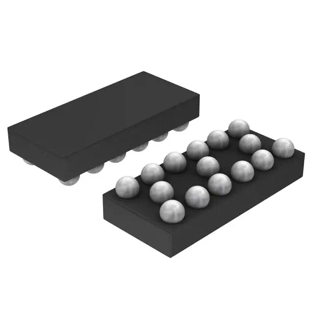
static discharges to protect delicate data line circuitry. It is offered in
300 �m and 350 �m solder spheres.
http://onsemi.com
CIRCUIT DESCRIPTION
A1
D1
Features
•
•
•
•
•
•
EMI Filtering and ESD Protection for Data Lines
Integration of 26 Discretes Offers Cost and Space Savings
Exceeds IEC61000−4−2 (Level 4) Specifications
Low Profile Flip−Chip Packaging
MSL 1
300 �m Solder Spheres (NUF4105), Case 499D
C1
C2
D2
C4
D4
R2
A2
C2
D3
C3
B1
R3
A3
C3
D5
C5
C6
D6
C8
D8
R4
Typical Applications
•
•
•
•
•
C1
A4
EMI Filtering and ESD Protection for Data Lines
Cell Phones
Handheld Portables
Notebook Computers
MP3 Players
C4
D7
C7
B2
R5
A5
C5
D9
C9 C10
D10
A6
MAXIMUM RATINGS (TA = 25°C)
Rating
C6
D11
Symbol
Value
C11 C12
D12
Unit
ESD Discharge IEC61000−4−2,
− Air Discharge
− Contact Discharge
Human Body Model
VPP
DC Power per Resistor
PR
100
mW
DC Power per Package
PT
400
mW
Junction Temperature
TJ
150
°C
Operating Temperature Range
Top
−40 to +85
°C
Storage Temperature Range
Tstg
−55 to +150
°C
B3
kV
30
30
16
A1
FLIP−CHIP
CASE 499D
300 �m Bumps
DEVICE MARKING
ON
NUF4105YYWW
Maximum ratings are those values beyond which device damage can occur.
Maximum ratings applied to the device are individual stress limit values (not
normal operating conditions) and are not valid simultaneously. If these limits are
exceeded, device functional operation is not implied, damage may occur and
reliability may be affected.
YY = Year
WW = Work Week
ORDERING INFORMATION
Device
Package
Shipping†
NUF4105FCT1
Flip−Chip
3000/Tape & Reel
†For information on tape and reel specifications,
including part orientation and tape sizes, please
refer to our Tape and Reel Packaging Specification
Brochure, BRD8011/D.
Semiconductor Components Industries, LLC, 2004
November, 2004 − Rev. 1
1
Publication Order Number:
NUF4105FC/D
�NUF4105FC
ELECTRICAL CHARACTERISTICS (TA = 25°C unless otherwise noted)
Symbol
Min
Typ
Max
Unit
6.0
7.0
8.0
V
VRM = 3.3 V per line
−
−
0.1
�A
RI/O
IR = 20 mA
80
100
120
�
Cline
VR = 2.5 V, f = 1.0 MHz (Note 1)
−
53
−
pF
VBR
Characteristic
IZ = 10 mA
IR
1. Measured from input/output pins to ground.
TYPICAL PERFORMANCE CURVES
(TA = 25°C unless otherwise specified)
0
0
−5
−10
−10
−20
S41 (dB)
−20
−25
Channel 2 or Channel 5
−30
−30
−40
Channel 3 to Channel 4
−50
−35
−60
−40
−70
−45
Channel 3 or Channel 4
−50
10
100
1000
10000
−80
10
100
FREQUENCY (MHz)
Figure 2. Analog Crosstalk Curve
105
104
103
102
101
100
99
98
97
96
95
−40
1000
FREQUENCY (MHz)
Figure 1. Insertion Loss Curve
RESISTANCE (�)
S21 (dB)
−15
−15
10
35
60
TEMPERATURE (°C)
Figure 3. Resistance Over Temperature
http://onsemi.com
2
85
10000
�NUF4105FC
2 V/div
Figure 4. ESD Response for Human Body Model (+8.0 kV)
500 mV/div
Figure 5. ESD Response for Human Body Model (−8.0 kV)
http://onsemi.com
3
�NUF4105FC
Printed Circuit Board Recommendations
500 �m Pitch
300 or 350 �m Solder Ball
Parameter
250 �m +25
250 �m −0
PCB Pad Size
Pad Shape
Round
Pad Type
NSMD
350 �m ±25
Solder Mask Opening
125 �m
Solder Stencil Thickness
Stencil Aperture
250 x 250 �m sq.
Solder Flux Ratio
50/50
Solder Paste Type
No Clean Type 3 or Finer
Trace Finish
OSP Cu
Trace Width
150 �m Max
Copper
Solder Mask
NSMD
SMD
Figure 6. Solder Mask versus Non−Solder Mask Definition
Controlled Atmosphere
250
225°C Min
235°C Max
TEMPERATURE (°C)
200
183 °C
2 to 5 °C/s
150
140 to 160 °C
100
50
1 to 5 °C/s
0
0
1
2
3
4
1 to 2 min
30−100 sec
TIME (minutes)
Figure 7. Solder Reflow Profile
http://onsemi.com
4
5
�NUF4105FC
PACKAGE DIMENSIONS
15 PIN FLIP−CHIP CSP
CASE 499D−01
ISSUE O
4X
0.10 C
TERMINAL A1
LOCATOR
ÈÈ
ÈÈ
D
A
NOTES:
1. DIMENSIONING AND TOLERANCING PER
ASME Y14.5M, 1994.
2. CONTROLLING DIMENSION: MILLIMETER.
3. COPLANARITY APPLIES TO SPHERICAL
CROWNS OF SOLDER BALLS.
B
E
A1
0.10 C
A2
A
C
0.05 C
SEATING
PLANE
D1
e /2
e
C
15 X
b
0.05 C A B
0.03 C
E1
B
A
1
2
3
4
5
6
e1
http://onsemi.com
5
DIM
A
A1
A2
D
E
b
e
e1
D1
E1
MILLIMETERS
MIN
MAX
−−−
0.700
0.210
0.270
0.380
0.430
2.960 BSC
1.330 BSC
0.290
0.340
0.500 BSC
0.435 BSC
2.500 BSC
0.870 BSC
�NUF4105FC
ON Semiconductor and
are registered trademarks of Semiconductor Components Industries, LLC (SCILLC). SCILLC reserves the right to make changes without further notice
to any products herein. SCILLC makes no warranty, representation or guarantee regarding the suitability of its products for any particular purpose, nor does SCILLC assume any liability
arising out of the application or use of any product or circuit, and specifically disclaims any and all liability, including without limitation special, consequential or incidental damages.
“Typical” parameters which may be provided in SCILLC data sheets and/or specifications can and do vary in different applications and actual performance may vary over time. All
operating parameters, including “Typicals” must be validated for each customer application by customer’s technical experts. SCILLC does not convey any license under its patent rights
nor the rights of others. SCILLC products are not designed, intended, or authorized for use as components in systems intended for surgical implant into the body, or other applications
intended to support or sustain life, or for any other application in which the failure of the SCILLC product could create a situation where personal injury or death may occur. Should
Buyer purchase or use SCILLC products for any such unintended or unauthorized application, Buyer shall indemnify and hold SCILLC and its officers, employees, subsidiaries, affiliates,
and distributors harmless against all claims, costs, damages, and expenses, and reasonable attorney fees arising out of, directly or indirectly, any claim of personal injury or death
associated with such unintended or unauthorized use, even if such claim alleges that SCILLC was negligent regarding the design or manufacture of the part. SCILLC is an Equal
Opportunity/Affirmative Action Employer. This literature is subject to all applicable copyright laws and is not for resale in any manner.
PUBLICATION ORDERING INFORMATION
LITERATURE FULFILLMENT:
Literature Distribution Center for ON Semiconductor
P.O. Box 61312, Phoenix, Arizona 85082−1312 USA
Phone: 480−829−7710 or 800−344−3860 Toll Free USA/Canada
Fax: 480−829−7709 or 800−344−3867 Toll Free USA/Canada
Email: orderlit@onsemi.com
N. American Technical Support: 800−282−9855 Toll Free
USA/Canada
ON Semiconductor Website: http://onsemi.com
Order Literature: http://www.onsemi.com/litorder
Japan: ON Semiconductor, Japan Customer Focus Center
2−9−1 Kamimeguro, Meguro−ku, Tokyo, Japan 153−0051
Phone: 81−3−5773−3850
http://onsemi.com
6
For additional information, please contact your
local Sales Representative.
NUF4105FC/D
�