ON Semiconductor
Is Now
To learn more about onsemi™, please visit our website at
www.onsemi.com
onsemi and and other names, marks, and brands are registered and/or common law trademarks of Semiconductor Components Industries, LLC dba “onsemi” or its affiliates and/or
subsidiaries in the United States and/or other countries. onsemi owns the rights to a number of patents, trademarks, copyrights, trade secrets, and other intellectual property. A listing of onsemi
product/patent coverage may be accessed at www.onsemi.com/site/pdf/Patent-Marking.pdf. onsemi reserves the right to make changes at any time to any products or information herein, without
notice. The information herein is provided “as-is” and onsemi makes no warranty, representation or guarantee regarding the accuracy of the information, product features, availability, functionality,
or suitability of its products for any particular purpose, nor does onsemi assume any liability arising out of the application or use of any product or circuit, and specifically disclaims any and all
liability, including without limitation special, consequential or incidental damages. Buyer is responsible for its products and applications using onsemi products, including compliance with all laws,
regulations and safety requirements or standards, regardless of any support or applications information provided by onsemi. “Typical” parameters which may be provided in onsemi data sheets and/
or specifications can and do vary in different applications and actual performance may vary over time. All operating parameters, including “Typicals” must be validated for each customer application
by customer’s technical experts. onsemi does not convey any license under any of its intellectual property rights nor the rights of others. onsemi products are not designed, intended, or authorized
for use as a critical component in life support systems or any FDA Class 3 medical devices or medical devices with a same or similar classification in a foreign jurisdiction or any devices intended for
implantation in the human body. Should Buyer purchase or use onsemi products for any such unintended or unauthorized application, Buyer shall indemnify and hold onsemi and its officers, employees,
subsidiaries, affiliates, and distributors harmless against all claims, costs, damages, and expenses, and reasonable attorney fees arising out of, directly or indirectly, any claim of personal injury or death
associated with such unintended or unauthorized use, even if such claim alleges that onsemi was negligent regarding the design or manufacture of the part. onsemi is an Equal Opportunity/Affirmative
Action Employer. This literature is subject to all applicable copyright laws and is not for resale in any manner. Other names and brands may be claimed as the property of others.
�NUF8000MU
Low Capacitance 8 Line EMI
Filter with ESD Protection in
UDFN Package
This device is an 8 line EMI filter array for wireless applications.
Greater than -30 dB typical attenuation is obtained at frequencies from
800 MHz to 5.0 GHz. The NUF8000MU has a typical cut-off frequency
of 95 MHz. This UDFN package is specifically designed to enhance EMI
filtering for low-profile or slim design electronics especially where space
and height is a premium. It also offers ESD protection-clamping
transients from static discharges. ESD protection is provided across all
capacitors.
Features
http://onsemi.com
16
1
Cd
Cd
2
15
Cd
Cd
3
•�EMI Filtering and ESD Protection
•�Integration of 40 Discrete Components
•�Compliance with IEC61000-4-2 (Level 4)
•�UDFN Package, 1.2 x 3.5 mm, 0.4 mm Pitch
•�Moisture Sensitivity Level 1
•�ESD Ratings: Machine Model = C
14
Cd
Cd
4
13
Cd
Cd
Cd
Cd
5
Human Body Model = 3B
12
6
11
•�This is a Pb-Free Device*
Cd
Benefits
Cd
10
7
•�Reduces EMI/RFI Emissions on a Data Line
•�Low Profile Package; Typical Height of 0.5 mm
•�Design-Friendly and Easy-to-Use Pin Configurations,
Cd
Cd
8
9
Cd
Particularly for Portable Electronics
•�Integrated Solution Offers Cost and Space Savings in UDFN Package
•�Reduces Parasitic Inductances Which Offer a More “Ideal” Low Pass
Filter Response
•�Integrated Solution Improves System Reliability
Cd
(Top View)
MARKING
DIAGRAM
16
1
Applications
800 M
G
UDFN16
MU SUFFIX
CASE 517AF
•�EMI Filtering and ESD Protection for Data Lines
•�Keypad Interface and Protection for Portable Electronics
•�Bottom Connector Interface for Mobile Handsets
•�Notebook Computers and Digital Cameras
•�LCD Display Interface in Mobile Handsets
•�Camera Display Interface in Mobile Handsets
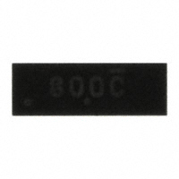
800
M
G
1
= Specific Device Code
= Date and Assembly Location
= Pb-Free Package
ORDERING INFORMATION
*For additional information on our Pb-Free strategy and soldering details, please
download the ON Semiconductor Soldering and Mounting Techniques
Reference Manual, SOLDERRM/D.
©� Semiconductor Components Industries, LLC, 2007
October, 2007 - Rev. 0
1
Device
Package
Shipping†
NUF8000MUT2G
UDFN16
(Pb-Free)
3000 / Tape & Reel
†For information on tape and reel specifications,
including part orientation and tape sizes, please
refer to our Tape and Reel Packaging Specifications
Brochure, BRD8011/D.
Publication Order Number:
NUF8000MU/D
�NUF8000MU
MAXIMUM RATINGS
Parameter
Symbol
ESD Discharge IEC61000-4-2
Value
VPP
Unit
kV
Contact Discharge
8.0
Operating Temperature Range
TOP
-40 to 85
°C
Storage Temperature Range
TSTG
-55 to 150
°C
TL
260
°C
Maximum Lead Temperature for Soldering Purposes (1.8 in from case for 10 seconds)
Stresses exceeding Maximum Ratings may damage the device. Maximum Ratings are stress ratings only. Functional operation above the
Recommended Operating Conditions is not implied. Extended exposure to stresses above the Recommended Operating Conditions may affect
device reliability.
ELECTRICAL CHARACTERISTICS (TJ = 25°C unless otherwise noted)
Parameter
Maximum Reverse Working Voltage
Breakdown Voltage
Symbol
Test Conditions
Min
Typ
VRWM
VBR
IR = 1.0 mA
Leakage Current
IR
VRWM = 3.3 V
Resistance
RA
IR = 20 mA
Capacitance (Notes 1 and 2)
Cd
Cut-Off Frequency (Note 3)
f3dB
Above this frequency,
appreciable attenuation occurs
1. Measured at 25°C, VR = 2.5 V, f = 1.0 MHz.
2. Total Line Capacitance is 2 times the Diode Capacitance (Cd).
3. 50 � source and 50 � load termination.
http://onsemi.com
2
Max
Unit
5.0
V
8.0
V
6.0
7.0
100
nA
85
100
115
�
15
20
pF
95
MHz
�NUF8000MU
TYPICAL PERFORMANCE CURVES (TA= 25°C unless otherwise specified)
0
0
-5
-10
-10
-20
-30
S41 (dB)
S21 (dB)
-15
-20
-25
-30
-50
-60
-35
-70
-40
-45
1.E+06
1.E+07
1.E+08
1.E+09
-80
10.0E+6
1.E+10
1.0E+9
10.0E+9
FREQUENCY (Hz)
Figure 1. Typical Insertion Loss Characteristic
Figure 2. Typical Analog Crosstalk
2
1.05
1.5
1.025
1
0.5
1
2
3
4
1
0.975
0.95
-40
0
0
100.0E+6
FREQUENCY (Hz)
RESISTANCE (�)
NORMALIZED CAPACITANCE
-40
5
-20
0
20
40
60
80
REVERSE VOLTAGE (V)
TEMPERATURE (°C)
Figure 3. Typical Capacitance vs.
Reverse Biased Voltage
(Normalized Capacitance Cd at 2.5 V)
Figure 4. Typical Resistance over Temperature
http://onsemi.com
3
�NUF8000MU
PACKAGE DIMENSIONS
UDFN16, 3.5x1.2, 0.4P
CASE 517AF-01
ISSUE B
0.10 C
PIN ONE
REFERENCE
2X
ÉÉÉÉ
ÉÉÉÉ
0.10 C
ÉÉ
ÇÇ
ÉÉ
A
B
D
2X
E
A1
A3
NOTES:
1. DIMENSIONING AND TOLERANCING PER
ASME Y14.5M, 1994.
2. CONTROLLING DIMENSION: MILLIMETERS.
3. DIMENSION b APPLIES TO PLATED TERMINAL
AND IS MEASURED BETWEEN 0.25 AND
0.30 mm FROM TERMINAL.
4. COPLANARITY APPLIES TO THE EXPOSED
PAD AS WELL AS THE TERMINALS.
DETAIL A
TOP VIEW
(A3)
DETAIL A
DIM
A
A1
A3
b
D
D2
E
E2
e
K
L
A
0.10 C
16X
SEATING
PLANE
0.08 C
SIDE VIEW
D2
16X
C
A1
14X
SOLDERING FOOTPRINT*
e
L
8
1
1.35
E2
1
16X
K
16
9
BOTTOM VIEW
16X
MILLIMETERS
MIN
NOM MAX
0.45
0.50
0.55
0.00
0.03
0.05
0.127 REF
0.15
0.20
0.25
3.50 BSC
2.70
2.80
2.90
1.20 BSC
0.20
0.30
0.40
0.40 BSC
0.20
----0.20
0.25
0.30
b
0.10 C A B
0.05 C
0.35
0.30
NOTE 3
0.10
2.85
15X
0.40 PITCH
0.20
16X
0.32
DIMENSIONS: MILLIMETERS
*For additional information on our Pb-Free strategy and soldering
details, please download the ON Semiconductor Soldering and
Mounting Techniques Reference Manual, SOLDERRM/D.
ON Semiconductor and
are registered trademarks of Semiconductor Components Industries, LLC (SCILLC). SCILLC reserves the right to make changes without further notice
to any products herein. SCILLC makes no warranty, representation or guarantee regarding the suitability of its products for any particular purpose, nor does SCILLC assume any liability
arising out of the application or use of any product or circuit, and specifically disclaims any and all liability, including without limitation special, consequential or incidental damages.
“Typical” parameters which may be provided in SCILLC data sheets and/or specifications can and do vary in different applications and actual performance may vary over time. All
operating parameters, including “Typicals” must be validated for each customer application by customer's technical experts. SCILLC does not convey any license under its patent rights
nor the rights of others. SCILLC products are not designed, intended, or authorized for use as components in systems intended for surgical implant into the body, or other applications
intended to support or sustain life, or for any other application in which the failure of the SCILLC product could create a situation where personal injury or death may occur. Should
Buyer purchase or use SCILLC products for any such unintended or unauthorized application, Buyer shall indemnify and hold SCILLC and its officers, employees, subsidiaries, affiliates,
and distributors harmless against all claims, costs, damages, and expenses, and reasonable attorney fees arising out of, directly or indirectly, any claim of personal injury or death
associated with such unintended or unauthorized use, even if such claim alleges that SCILLC was negligent regarding the design or manufacture of the part. SCILLC is an Equal
Opportunity/Affirmative Action Employer. This literature is subject to all applicable copyright laws and is not for resale in any manner.
PUBLICATION ORDERING INFORMATION
LITERATURE FULFILLMENT:
Literature Distribution Center for ON Semiconductor
P.O. Box 5163, Denver, Colorado 80217 USA
Phone: 303-675-2175 or 800-344-3860 Toll Free USA/Canada
Fax: 303-675-2176 or 800-344-3867 Toll Free USA/Canada
Email: orderlit@onsemi.com
N. American Technical Support: 800-282-9855 Toll Free
USA/Canada
Europe, Middle East and Africa Technical Support:
Phone: 421 33 790 2910
Japan Customer Focus Center
Phone: 81-3-5773-3850
http://onsemi.com
4
ON Semiconductor Website: www.onsemi.com
Order Literature: http://www.onsemi.com/orderlit
For additional information, please contact your local
Sales Representative
NUF8000MU/D
�