NUP1128, NUP2128
Single Line LIN & Dual Line
CAN Bus Protector
The NUP1128/NUP2128 are designed to protect both CAN and LIN
transceivers from ESD and other harmful transient voltage events.
These devices provide bidirectional protection for each data line with
a single compact SC−70 (SOT−323) or SOD−323 package, giving the
system designer a low cost option for improving system reliability and
meeting stringent EMI requirements.
www.onsemi.com
MARKING
DIAGRAMS
Features
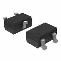
SC−70
CASE 419
• Low Reverse Leakage Current (< 100 nA)
• 175°C TJ(max) − Rated for High Temperature, Mission Critical
•
•
•
•
•
•
Applications
IEC Compatibility:
IEC 61000−4−2 (ESD): Level 4
IEC 61000−4−4 (EFT): 50 A (5/50 ns)
IEC 61000−4−5 (Lighting) 3.0 A (8/20 ms)
ISO 7637−1, Nonrepetitive EMI Surge Pulse 2, 8.0 A (1/50 ms)
ISO 7637−3, Repetitive Electrical Fast Transient (EFT)
EMI Surge Pulses, 50 A (5/50 ns)
Flammability Rating UL 94 V−0
SZ Prefix for Automotive and Other Applications Requiring Unique
Site and Control Change Requirements; AEC−Q101 Qualified and
PPAP Capable
These Devices are Pb−Free, Halogen Free/BFR Free and are RoHS
Compliant
1
2
XX
M
G
♦
♦
XX M
= Specific Device Code
= Date Code
= Pb−Free Package
(Note: Microdot may be in either location)
PIN 1
PIN 3
NUP1128
(SC−70)
PIN 1
PIN 2
NUP1128
(SOD−323)
• Automotive Networks
♦
SOD−323
CASE 477
1
Applications
♦
XX MG
G
CAN / CAN−FD
Low and High−Speed CAN
Fault Tolerant CAN
LIN
PIN 1
PIN 3
PIN 2
NUP2128
CAN_H / Single Wire LIN
CAN / LIN
Transceiver
CAN_L
NUP1128
CAN / LIN
NUP2128
ORDERING INFORMATION
See detailed ordering, marking and shipping information on
page 7 of this data sheet.
© Semiconductor Components Industries, LLC, 2017
March, 2019 − Rev. 0
1
Publication Order Number:
NUP1128/D
�NUP1128, NUP2128
MAXIMUM RATINGS (TJ = 25°C, unless otherwise specified)
Symbol
PPK
Rating
Peak Power Dissipation, 8/20 ms Double Exponential Waveform (Note 1)
Value
Unit
165
W
TJ
Operating Junction Temperature Range
NUP1128HT1G, SZNUP1128HT1G
All other devices
−55 to 150
−55 to 175
TJ
Storage Temperature Range
NUP1128HT1G, SZNUP1128HT1G
All other devices
−55 to 150
−55 to 175
TL
Lead Solder Temperature (10 s)
260
°C
Human Body Model (HBM)
IEC 61000−4−2 Contact
IEC 61000−4−2 Air
ISO 10605 Contact (330 pF / 330 W)
ISO 10605 Contact (330 pF / 2 kW)
ISO 10605 Contact (150 pF / 2 kW)
8.0
±30
±30
±30
±30
±30
kV
kV
kV
kV
kV
kV
ESD
°C
°C
Stresses exceeding those listed in the Maximum Ratings table may damage the device. If any of these limits are exceeded, device functionality
should not be assumed, damage may occur and reliability may be affected.
1. Non−repetitive current pulse per Figure 1.
ELECTRICAL CHARACTERISTICS (TJ = 25°C, unless otherwise specified)
Symbol
VRWM
Parameter
Test Conditions
Min
Typ
Max
Unit
26.5
V
31
35.5
V
Reverse Working Voltage
(Note 2)
Breakdown Voltage
IT = 1 mA (Note 3)
IR
Reverse Leakage Current
VRWM = 26.5 V
TA = 150°C
1
150
100
750
nA
VC
Clamping Voltage
IPP = 1 A (8/20 ms Waveform) (Note 4)
IPP = 3 A
39
46
47
55
V
IPP
Maximum Peak Pulse Current
8/20 ms Waveform (Note 4)
CJ
Capacitance
VR = 0 V, f = 1 MHz (Line to GND)
DC
Diode Capacitance Matching
VR = 0 V, f = 1 MHz (Note 5)
VBR
27.5
3.0
A
11
13
pF
2
%
Product parametric performance is indicated in the Electrical Characteristics for the listed test conditions, unless otherwise noted. Product
performance may not be indicated by the Electrical Characteristics if operated under different conditions.
2. TVS devices are normally selected according to the working peak reverse voltage (VRWM), which should be equal or greater than the DC
or continuous peak operating voltage level.
3. VBR is measured at pulse test current IT.
4. Pulse waveform per Figure 1.
5. DC is the percentage difference between CJ of lines 1 and 2 measured according to the test conditions given in the electrical characteristics
table.
www.onsemi.com
2
�NUP1128, NUP2128
TYPICAL PERFORMANCE CURVES
(TJ = 25°C unless otherwise noted)
1.E−02
12
1.E−03
10
1.E−04
1.E−05
8
C (pF)
I (A)
1.E−06
1.E−07
1.E−08
6
4
1.E−09
1.E−10
2
1.E−11
1.E−12
−40
−30
−20
−10
0
V (V)
10
30
20
0
−30 −25 −20 −15 −10 −5
5
0
VBias (V)
40
Figure 1. IV Characteristics
25
+55°C
+85°C
20
15
10
+150°C
5
0
1E−12
1E−11 1E−10 1E−09 1E−08
IL, LEAKAGE CURRENT (A)
1E−07
30
20
40
60
80
100
−60 −40 −20
1E−06
0 20 40 60 80 100 120 140 160 180
TEMPERATURE (°C)
Figure 4. Temperature Power Dissipation Derating
Figure 3. IR vs Temperature Characteristics
60
110
WAVEFORM
PARAMETERS
tr = 8 ms
td = 20 ms
100
90
80
c−t
70
50
VCLAMP, (V)
% OF PEAK PULSE CURRENT
20 25
0
+25°C
−55°C
15
Figure 2. CV Characteristics
PERCENT DERATING (%)
VR, REVERSE BIAS VOLTAGE (V)
30
10
60
td = IPP/2
50
40
30
20
40
IO−GND
30
20
10
10
0
0
5
10
15
20
25
0
30
0
1
2
3
IPP (A)
t, TIME (ms)
Figure 6. Clamping Voltage vs Peak Pulse Current
(8/20 ms)
Figure 5. Pulse Waveform (8/20 ms)
www.onsemi.com
3
4
�180
20
160
0
140
−20
120
−40
VOLTAGE (V)
VOLTAGE (V)
NUP1128, NUP2128
100
80
60
40
−60
−80
−100
−120
20
−140
0
−160
−20
−20
0
20
40
60
80
TIME (ns)
100
120
140
−180
−20
Figure 7. IEC61000−4−2 +8 kV Contact ESD
Clamping Voltage
0
20
40
60
80
TIME (ns)
100
120
Figure 8. IEC61000−4−2 −8 kV Contact ESD
Clamping Voltage
www.onsemi.com
4
140
�NUP1128, NUP2128
IEC61000−4−2 Waveform
IEC 61000−4−2 Spec.
Ipeak
Level
Test Voltage (kV)
First Peak
Current
(A)
Current at
30 ns (A)
Current at
60 ns (A)
1
2
7.5
4
2
2
4
15
8
4
3
6
22.5
12
6
4
8
30
16
8
100%
90%
I @ 30 ns
I @ 60 ns
10%
tP = 0.7 ns to 1 ns
Figure 9. IEC61000−4−2 Spec
Device
ESD Gun
Under
Oscilloscope
Test
50 W
50 W
Cable
Figure 10. Diagram of ESD Clamping Voltage Test Setup
The following is taken from Application Note
AND8308/D − Interpretation of Datasheet Parameters
for ESD Devices.
systems such as cell phones or laptop computers it is not
clearly defined in the spec how to specify a clamping voltage
at the device level. ON Semiconductor has developed a way
to examine the entire voltage waveform across the ESD
protection diode over the time domain of an ESD pulse in the
form of an oscilloscope screenshot, which can be found on
the datasheets for all ESD protection diodes. For more
information on how ON Semiconductor creates these
screenshots and how to interpret them please refer to
AND8307/D.
ESD Voltage Clamping
For sensitive circuit elements it is important to limit the
voltage that an IC will be exposed to during an ESD event
to as low a voltage as possible. The ESD clamping voltage
is the voltage drop across the ESD protection diode during
an ESD event per the IEC61000−4−2 waveform. Since the
IEC61000−4−2 was written as a pass/fail spec for larger
www.onsemi.com
5
�NUP1128, NUP2128
20
10
18
14
−14
6
12
10
6
−12
−10
4
8
6
2
4
4
−8
−6
−4
2
−2
2
NOTE:
8
−16
EQUIVALENT VIEC (kV)
TLP CURRENT (A)
TLP CURRENT (A)
8
EQUIVALENT VIEC (kV)
−18
16
0
0
10
−20
10
20
30
40
0
0
0
50
10
20
30
40
VOLTAGE (V)
VOLTAGE (V)
Figure 11. Positive TLP IV Curve
Figure 12. Negative TLP IV Curve
0
50
TLP parameter: Z0 = 50 W, tp = 100 ns, tr = 300 ps, averaging window: t1 = 30 ns to t2 = 60 ns.
Transmission Line Pulse (TLP) Measurement
L
Transmission Line Pulse (TLP) provides current versus
voltage (I−V) curves in which each data point is obtained
from a 100 ns long rectangular pulse from a charged
transmission line. A simplified schematic of a typical TLP
system is shown in Figure 13. TLP I−V curves of ESD
protection devices accurately demonstrate the product’s
ESD capability because the 10s of amps current levels and
under 100 ns time scale match those of an ESD event. This
is illustrated in Figure 14 where an 8 kV IEC 61000−4−2
current waveform is compared with TLP current pulses at
8 A and 16 A. A TLP I−V curve shows the voltage at which
the device turns on as well as how well the device clamps
voltage over a range of current levels.
50 W Coax
Cable
S Attenuator
÷
50 W Coax
Cable
10 MW
IM
VM
DUT
VC
Oscilloscope
Figure 13. Simplified Schematic of a Typical TLP
System
Figure 14. Comparison Between 8 kV IEC 61000−4−2 and 8 A and 16 A TLP Waveforms
www.onsemi.com
6
�NUP1128, NUP2128
ORDERING INFORMATION
Device
NUP1128WTT1G
SZNUP1128WTT1G*
NUP2128WTT1G
SZNUP2128WTT1G*
NUPH1128HT1G
(In Development**)
SZNUPH1128HT1G*
(In Development**)
NUP1128HT1G
SZNUP1128HT1G*
Marking
Package
Operating Junction
Temperature Range
Shipping†
7X
SC−70
(Pb−Free)
7U
3000 / Tape & Reel
−55 to 175°C
TBD
SOD−323
(Pb−Free)
7A
3000 / Tape & Reel
−55 to 150°C
†For information on tape and reel specifications, including part orientation and tape sizes, please refer to our Tape and Reel Packaging
Specifications Brochure, BRD8011/D.
*SZ Prefix for Automotive and Other Applications Requiring Unique Site and Control Change Requirements; AEC−Q101 Qualified and PPAP
Capable.
**Product release in Q3 2019.
www.onsemi.com
7
�NUP1128, NUP2128
PACKAGE DIMENSIONS
SC−70 (SOT−323)
CASE 419−04
ISSUE N
D
NOTES:
1. DIMENSIONING AND TOLERANCING PER ANSI Y14.5M, 1982.
2. CONTROLLING DIMENSION: INCH.
e1
DIM
A
A1
A2
b
c
D
E
e
e1
L
HE
3
E
HE
1
2
b
e
A
0.05 (0.002)
MIN
0.80
0.00
0.30
0.10
1.80
1.15
1.20
0.20
2.00
MILLIMETERS
NOM
MAX
0.90
1.00
0.05
0.10
0.70 REF
0.35
0.40
0.18
0.25
2.10
2.20
1.24
1.35
1.30
1.40
0.65 BSC
0.38
0.56
2.10
2.40
c
A2
L
A1
SOLDERING FOOTPRINT*
0.65
0.025
0.65
0.025
1.9
0.075
0.9
0.035
0.7
0.028
SCALE 10:1
mm Ǔ
ǒinches
*For additional information on our Pb−Free strategy and soldering
details, please download the ON Semiconductor Soldering and
Mounting Techniques Reference Manual, SOLDERRM/D.
www.onsemi.com
8
MIN
0.032
0.000
0.012
0.004
0.071
0.045
0.047
0.008
0.079
INCHES
NOM
0.035
0.002
0.028 REF
0.014
0.007
0.083
0.049
0.051
0.026 BSC
0.015
0.083
MAX
0.040
0.004
0.016
0.010
0.087
0.053
0.055
0.022
0.095
�NUP1128, NUP2128
PACKAGE DIMENSIONS
SOD−323
CASE 477−02
ISSUE H
NOTES:
1. DIMENSIONING AND TOLERANCING PER ANSI
Y14.5M, 1982.
2. CONTROLLING DIMENSION: MILLIMETERS.
3. LEAD THICKNESS SPECIFIED PER L/F DRAWING
WITH SOLDER PLATING.
4. DIMENSIONS A AND B DO NOT INCLUDE MOLD
FLASH, PROTRUSIONS OR GATE BURRS.
5. DIMENSION L IS MEASURED FROM END OF RADIUS.
HE
D
b
1
2
E
A3
A
C
NOTE 3
L
MILLIMETERS
DIM MIN
NOM MAX
A
0.80
0.90
1.00
A1 0.00
0.05
0.10
A3
0.15 REF
b
0.25
0.32
0.4
C 0.089
0.12 0.177
D
1.60
1.70
1.80
E
1.15
1.25
1.35
L
0.08
HE
2.30
2.50
2.70
INCHES
NOM MAX
0.035 0.040
0.002 0.004
0.006 REF
0.010 0.012 0.016
0.003 0.005 0.007
0.062 0.066 0.070
0.045 0.049 0.053
0.003
0.090 0.098 0.105
MIN
0.031
0.000
A1
NOTE 5
SOLDERING FOOTPRINT*
0.63
0.025
0.83
0.033
1.60
0.063
2.85
0.112
*For additional information on our Pb−Free strategy and soldering
details, please download the ON Semiconductor Soldering and
Mounting Techniques Reference Manual, SOLDERRM/D.
Honeywell and SDS are registered trademarks of Honeywell International Inc.
DeviceNet is a trademark of Rockwell Automation.
ON Semiconductor and
are trademarks of Semiconductor Components Industries, LLC dba ON Semiconductor or its subsidiaries in the United States and/or other countries.
ON Semiconductor owns the rights to a number of patents, trademarks, copyrights, trade secrets, and other intellectual property. A listing of ON Semiconductor’s product/patent
coverage may be accessed at www.onsemi.com/site/pdf/Patent−Marking.pdf. ON Semiconductor reserves the right to make changes without further notice to any products herein.
ON Semiconductor makes no warranty, representation or guarantee regarding the suitability of its products for any particular purpose, nor does ON Semiconductor assume any liability
arising out of the application or use of any product or circuit, and specifically disclaims any and all liability, including without limitation special, consequential or incidental damages.
Buyer is responsible for its products and applications using ON Semiconductor products, including compliance with all laws, regulations and safety requirements or standards,
regardless of any support or applications information provided by ON Semiconductor. “Typical” parameters which may be provided in ON Semiconductor data sheets and/or
specifications can and do vary in different applications and actual performance may vary over time. All operating parameters, including “Typicals” must be validated for each customer
application by customer’s technical experts. ON Semiconductor does not convey any license under its patent rights nor the rights of others. ON Semiconductor products are not
designed, intended, or authorized for use as a critical component in life support systems or any FDA Class 3 medical devices or medical devices with a same or similar classification
in a foreign jurisdiction or any devices intended for implantation in the human body. Should Buyer purchase or use ON Semiconductor products for any such unintended or unauthorized
application, Buyer shall indemnify and hold ON Semiconductor and its officers, employees, subsidiaries, affiliates, and distributors harmless against all claims, costs, damages, and
expenses, and reasonable attorney fees arising out of, directly or indirectly, any claim of personal injury or death associated with such unintended or unauthorized use, even if such
claim alleges that ON Semiconductor was negligent regarding the design or manufacture of the part. ON Semiconductor is an Equal Opportunity/Affirmative Action Employer. This
literature is subject to all applicable copyright laws and is not for resale in any manner.
PUBLICATION ORDERING INFORMATION
LITERATURE FULFILLMENT:
Literature Distribution Center for ON Semiconductor
19521 E. 32nd Pkwy, Aurora, Colorado 80011 USA
Phone: 303−675−2175 or 800−344−3860 Toll Free USA/Canada
Fax: 303−675−2176 or 800−344−3867 Toll Free USA/Canada
Email: orderlit@onsemi.com
◊
N. American Technical Support: 800−282−9855 Toll Free
USA/Canada
Europe, Middle East and Africa Technical Support:
Phone: 421 33 790 2910
www.onsemi.com
9
ON Semiconductor Website: www.onsemi.com
Order Literature: http://www.onsemi.com/orderlit
For additional information, please contact your local
Sales Representative
NUP1128/D
�