NV8664ST50T3GEVB
NCV8664 Evaluation Board
User's Manual
http://onsemi.com
EVAL BOARD USER’S MANUAL
Description
• Wide Input Voltage Operating Range of 5.5 V to 45 V
• Internal Fault Protection
• −42 V Reverse Voltage
• Short Circuit/Overcurrent
• Thermal Overload
The NCV8664 is a precision 3.3 V and 5.0 V fixed output,
low dropout integrated voltage regulator with an output
current capability of 150 mA. Careful management of light
load current consumption, combined with a low leakage
process, achieve a typical quiescent ground current of
22 mA. The output voltage is accurate within ±2.0%, and
maximum dropout voltage is 600 mV at full rated load
current. The following ceramic capacitors are the
recommended values to be used with these devices; Cin =
0.1 mF, Cout = 10 mF.
Board Notes
Max voltage on Vin cap not to exceed 35 V.
Board Layouts
These boards are shown in sets of 2 due to the minimum
board size requirement of most board fabrication houses.
When sent out for fabrication, it must be indicated that the
center line of the board set be V−scored to allow board
separation.
Features
• ±2.0% Output Accuracy, Over Full Temperature Range
• 30 mA Maximum Quiescent Current at Iout = 100 mA
• 600 mV Maximum Dropout Voltage at 150 mA Load
Current
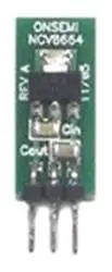
Figure 1. Evaluation Board Photo
© Semiconductor Components Industries, LLC, 2012
May, 2012 − Rev. 1
1
Publication Order Number:
EVBUM2117/D
�NV8664ST50T3GEVB
Figure 2. SOT−223 Evaluation Board
Figure 3. DPAK Evaluation Board
SCHEMATIC FOR THE NCV8664 EVALUATION BOARD
NCV8664 Demo Board
Vin
NCV8664
Vout
Cin
Cout
Figure 4. NCV8664 Evaluation Board Circuit
http://onsemi.com
2
�NV8664ST50T3GEVB
Lead Free
−
−
Advanced Circuits
NCV8664DPAK3DemoBoard
No
Yes
−
SOT223
On Semiconductor
NCV8664ST50R3G
No
Yes
−
−
−
Molex/Waldom Electronics Corporation
22−28−8030
Yes
Yes
0.1 mF
10%
1206
Murata Electronics North America
GRM319R71H104KA01D
Yes
Yes
10 mF
10%
1206
Murata Electronics North America
GRM31CR71C106KAC7L
Yes
Yes
Value
Footprint
−
−
Tolerance
Substitution
Allowed
Table 1. BILL OF MATERIALS FOR THE NCV8664 EVALUATION BOARD
Manufacturer
Part Number
SOT223 BOM
DPAK BOM
−
−
−
Advanced Circuits
NCV8664DPAK3DemoBoard
No
Yes
−
−
DPAK
On Semiconductor
NCV8664DT50RKG
No
Yes
−
−
−
Molex/Waldom Electronics Corporation
22−28−8030
Yes
Yes
0.1 mF
10%
1206
Murata Electronics North America
GRM319R71H104KA01D
Yes
Yes
10 mF
10%
1206
Murata Electronics North America
GRM31CR71C106KAC7L
Yes
Yes
Test Procedure
Required Equipment:
• Resistive Load
• 2 Multimeters
• One NCV8664 Evaluation Board
• DC Power Supply
NCV8664 Demo Board
DC Power Supply
I
Vin
NCV8664
Vout
Cin
O
Cout
GND
Load
+
DC −
Voltmeter
+
−
DC
Voltmeter
G
Figure 5. Dropout Voltage Test Setup
Dropout Voltage Verification Steps
1. Connect circuit as shown in Figure 5.
2. Set Vin = 13.5 V, Record Vout.
3. Reduce Vin until Vout has dropped by 100 mV.
4. Subtract Vout from Vin. Resulting Voltage is
Dropout Voltage.
http://onsemi.com
3
�NV8664ST50T3GEVB
0.40
Quiescent Current Verification Steps
1. Connect circuit as shown in Figure 7.
2. Set Vin = 13.5 V.
3. Subtract Output Current from Input Current.
DROPOUT VOLTAGE (V)
0.35
0.30
0.25
0.20
0.15
0.10
0.05
0
0
50
100
200
150
OUTPUT CURRENT (mA)
Figure 6. Dropout Voltage vs. Output Current
DC
Ammeter
+
DC
Ammeter
+
−
NCV8664 Demo Board
DC Power Supply
Vin
I
NCV8664
Cin
Vout
O
Cout
GND
G
Figure 7. Quiescent Current Verification Setup
http://onsemi.com
4
Load
−
�NV8664ST50T3GEVB
Output Voltage Verification Steps
1. Connect circuit as shown in Figure 9.
2. Set output load to 100 W, Set Vin = 0 V, Record
Vout.
3. Increase Vin, measure Vout.
9
8
7
6
5
4
3
2
1
0
Vin = 13.5 V
0
50
100
200
150
OUTPUT CURRENT (mA)
Figure 8. Current Consumption vs. Output
Current
NCV8664 Demo Board
DC Power Supply
Vin
I
NCV8664
Vout
Cin
O
Cout
+
GND
Load
+
DC −
Voltmeter
G
Figure 9. Quiescent Current Verification Setup
6
5
OUTPUT VOLTAGE (V)
CURRENT CONSUMPTION (mA)
10
4
3
2
RL = 100 W
1
0
0
10
20
30
40
INPUT VOLTAGE (V)
Figure 10. Input Voltage vs. Output Voltage
http://onsemi.com
5
−
DC
Voltmeter
�onsemi,
, and other names, marks, and brands are registered and/or common law trademarks of Semiconductor Components Industries, LLC dba “onsemi” or its affiliates
and/or subsidiaries in the United States and/or other countries. onsemi owns the rights to a number of patents, trademarks, copyrights, trade secrets, and other intellectual property. A
listing of onsemi’s product/patent coverage may be accessed at www.onsemi.com/site/pdf/Patent−Marking.pdf. onsemi is an Equal Opportunity/Affirmative Action Employer. This
literature is subject to all applicable copyright laws and is not for resale in any manner.
The evaluation board/kit (research and development board/kit) (hereinafter the “board”) is not a finished product and is not available for sale to consumers. The board is only intended
for research, development, demonstration and evaluation purposes and will only be used in laboratory/development areas by persons with an engineering/technical training and familiar
with the risks associated with handling electrical/mechanical components, systems and subsystems. This person assumes full responsibility/liability for proper and safe handling. Any
other use, resale or redistribution for any other purpose is strictly prohibited.
THE BOARD IS PROVIDED BY ONSEMI TO YOU “AS IS” AND WITHOUT ANY REPRESENTATIONS OR WARRANTIES WHATSOEVER. WITHOUT LIMITING THE FOREGOING,
ONSEMI (AND ITS LICENSORS/SUPPLIERS) HEREBY DISCLAIMS ANY AND ALL REPRESENTATIONS AND WARRANTIES IN RELATION TO THE BOARD, ANY
MODIFICATIONS, OR THIS AGREEMENT, WHETHER EXPRESS, IMPLIED, STATUTORY OR OTHERWISE, INCLUDING WITHOUT LIMITATION ANY AND ALL
REPRESENTATIONS AND WARRANTIES OF MERCHANTABILITY, FITNESS FOR A PARTICULAR PURPOSE, TITLE, NON−INFRINGEMENT, AND THOSE ARISING FROM A
COURSE OF DEALING, TRADE USAGE, TRADE CUSTOM OR TRADE PRACTICE.
onsemi reserves the right to make changes without further notice to any board.
You are responsible for determining whether the board will be suitable for your intended use or application or will achieve your intended results. Prior to using or distributing any systems
that have been evaluated, designed or tested using the board, you agree to test and validate your design to confirm the functionality for your application. Any technical, applications or
design information or advice, quality characterization, reliability data or other services provided by onsemi shall not constitute any representation or warranty by onsemi, and no additional
obligations or liabilities shall arise from onsemi having provided such information or services.
onsemi products including the boards are not designed, intended, or authorized for use in life support systems, or any FDA Class 3 medical devices or medical devices with a similar
or equivalent classification in a foreign jurisdiction, or any devices intended for implantation in the human body. You agree to indemnify, defend and hold harmless onsemi, its directors,
officers, employees, representatives, agents, subsidiaries, affiliates, distributors, and assigns, against any and all liabilities, losses, costs, damages, judgments, and expenses, arising
out of any claim, demand, investigation, lawsuit, regulatory action or cause of action arising out of or associated with any unauthorized use, even if such claim alleges that onsemi was
negligent regarding the design or manufacture of any products and/or the board.
This evaluation board/kit does not fall within the scope of the European Union directives regarding electromagnetic compatibility, restricted substances (RoHS), recycling (WEEE), FCC,
CE or UL, and may not meet the technical requirements of these or other related directives.
FCC WARNING – This evaluation board/kit is intended for use for engineering development, demonstration, or evaluation purposes only and is not considered by onsemi to be a finished
end product fit for general consumer use. It may generate, use, or radiate radio frequency energy and has not been tested for compliance with the limits of computing devices pursuant
to part 15 of FCC rules, which are designed to provide reasonable protection against radio frequency interference. Operation of this equipment may cause interference with radio
communications, in which case the user shall be responsible, at its expense, to take whatever measures may be required to correct this interference.
onsemi does not convey any license under its patent rights nor the rights of others.
LIMITATIONS OF LIABILITY: onsemi shall not be liable for any special, consequential, incidental, indirect or punitive damages, including, but not limited to the costs of requalification,
delay, loss of profits or goodwill, arising out of or in connection with the board, even if onsemi is advised of the possibility of such damages. In no event shall onsemi’s aggregate liability
from any obligation arising out of or in connection with the board, under any theory of liability, exceed the purchase price paid for the board, if any.
The board is provided to you subject to the license and other terms per onsemi’s standard terms and conditions of sale. For more information and documentation, please visit
www.onsemi.com.
PUBLICATION ORDERING INFORMATION
LITERATURE FULFILLMENT:
Email Requests to: orderlit@onsemi.com
onsemi Website: www.onsemi.com
◊
TECHNICAL SUPPORT
North American Technical Support:
Voice Mail: 1 800−282−9855 Toll Free USA/Canada
Phone: 011 421 33 790 2910
www.onsemi.com
1
Europe, Middle East and Africa Technical Support:
Phone: 00421 33 790 2910
For additional information, please contact your local Sales Representative
�