ON Semiconductor
Is Now
To learn more about onsemi™, please visit our website at
www.onsemi.com
onsemi and and other names, marks, and brands are registered and/or common law trademarks of Semiconductor Components Industries, LLC dba “onsemi” or its affiliates and/or
subsidiaries in the United States and/or other countries. onsemi owns the rights to a number of patents, trademarks, copyrights, trade secrets, and other intellectual property. A listing of onsemi
product/patent coverage may be accessed at www.onsemi.com/site/pdf/Patent-Marking.pdf. onsemi reserves the right to make changes at any time to any products or information herein, without
notice. The information herein is provided “as-is” and onsemi makes no warranty, representation or guarantee regarding the accuracy of the information, product features, availability, functionality,
or suitability of its products for any particular purpose, nor does onsemi assume any liability arising out of the application or use of any product or circuit, and specifically disclaims any and all
liability, including without limitation special, consequential or incidental damages. Buyer is responsible for its products and applications using onsemi products, including compliance with all laws,
regulations and safety requirements or standards, regardless of any support or applications information provided by onsemi. “Typical” parameters which may be provided in onsemi data sheets and/
or specifications can and do vary in different applications and actual performance may vary over time. All operating parameters, including “Typicals” must be validated for each customer application
by customer’s technical experts. onsemi does not convey any license under any of its intellectual property rights nor the rights of others. onsemi products are not designed, intended, or authorized
for use as a critical component in life support systems or any FDA Class 3 medical devices or medical devices with a same or similar classification in a foreign jurisdiction or any devices intended for
implantation in the human body. Should Buyer purchase or use onsemi products for any such unintended or unauthorized application, Buyer shall indemnify and hold onsemi and its officers, employees,
subsidiaries, affiliates, and distributors harmless against all claims, costs, damages, and expenses, and reasonable attorney fees arising out of, directly or indirectly, any claim of personal injury or death
associated with such unintended or unauthorized use, even if such claim alleges that onsemi was negligent regarding the design or manufacture of the part. onsemi is an Equal Opportunity/Affirmative
Action Employer. This literature is subject to all applicable copyright laws and is not for resale in any manner. Other names and brands may be claimed as the property of others.
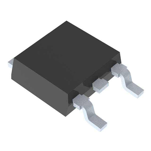
�NVATS4A101PZ
Power MOSFET
30 V, 30 mΩ, 27 A, P-Channel
The NVATS4A101PZ is a power MOSFET designed for compact size and
high efficiency which can achieve high thermal performance.
AEC-Q101 qualified MOSFET and PPAP capable suitable for automotive
applications.
www.onsemi.com
VDSS
Features
Low On-Resistance
High Current Capability
100% Avalanche Tested
AEC-Q101 qualified and PPAP capable
ATPAK package is pin-compatible with DPAK (TO-252)
Pb-Free, Halogen Free and RoHS compliance
30 V
RDS(on) Max
30 mΩ @ 10 V
51 mΩ @ 4.5 V
ID Max
27 A
ELECTRICAL CONNECTION
P-Channel
2,4
Typical Applications
Reverse Battery Protection
Load Switch
Automotive Front Lighting
Automotive Body Controllers
1
1 : Gate
2 : Drain
3 : Source
4 : Drain
SPECIFICATIONS
ABSOLUTE MAXIMUM RATING at Ta = 25C (Note 1)
Parameter
Drain to Source Voltage
Gate to Source Voltage
Drain Current (DC)
Drain Current (Pulse)
PW 10 s, duty cycle 1%
Power Dissipation
Tc = 25C
Operating Junction and
Storage Temperature
Symbol
VDSS
VGSS
ID
3
Value
30
20
27
Unit
V
V
A
IDP
81
A
PD
36
W
55 to +175
C
Tj, Tstg
4
1 2
3
ATPAK
MARKING
Avalanche Energy (Single Pulse) (Note 2)
EAS
25
mJ
Avalanche Current (Note 3)
IAV
13
A
Note 1 : Stresses exceeding those listed in the Maximum Ratings table may damage
the device. If any of these limits are exceeded, device functionality should not
be assumed, damage may occur and reliability may be affected.
2 : VDD = 10 V, L = 200 H, IAV = 13 A
3 : L ≤ 200 H, Single pulse
ORDERING INFORMATION
THERMAL RESISTANCE RATINGS
Parameter
Symbol
Junction to Case Steady State (Tc = 25C)
RJC
Junction to Ambient (Note 4)
RJA
Value
Unit
4.1
C/W
80.7
C/W
See detailed ordering and shipping
information on page 6 of this data sheet.
2
Note 4 : Surface mounted on FR4 board using a 130 mm , 1 oz. Cu pad.
© Semiconductor Components Industries, LLC, 2017
March 2017 - Rev. 0
1
Publication Order Number :
NVATS4A101PZ/D
�NVATS4A101PZ
ELECTRICAL CHARACTERISTICS at Ta 25C (Note 5)
Conditions
Value
Parameter
Symbol
Drain to Source Breakdown Voltage
V(BR)DSS
IDSS
ID = 1 mA, VGS = 0 V
Zero-Gate Voltage Drain Current
VDS = 30 V, VGS = 0 V
1
A
Gate to Source Leakage Current
IGSS
VGS = 16 V, VDS = 0 V
10
A
Gate Threshold Voltage
VGS(th)
VDS = 10 V, ID = 1 mA
2.6
V
Forward Transconductance
gFS
VDS = 10 V, ID = 13 A
17
Static Drain to Source On-State
Resistance
RDS(on)1
RDS(on)2
ID = 13 A, VGS = 10 V
23
30
mΩ
36
51
mΩ
Input Capacitance
Ciss
Output Capacitance
Coss
Reverse Transfer Capacitance
Turn-ON Delay Time
ID = 7 A, VGS = 4.5 V
min
typ
max
30
Unit
V
1.2
S
875
pF
220
pF
Crss
155
pF
td(on)
9.2
ns
Rise Time
tr
70
ns
Turn-OFF Delay Time
td(off)
80
ns
Fall Time
tf
Total Gate Charge
Qg
Gate to Source Charge
Qgs
Gate to Drain “Miller” Charge
Qgd
VDS = 10 V, f = 1 MHz
See Fig.1
VDS = 15 V, VGS = 10 V, ID = 25 A
70
ns
18.5
nC
3.2
nC
4.0
nC
VSD
IS = 25A, VGS = 0 V
Forward Diode Voltage
V
0.99
1.5
Note 5 : Product parametric performance is indicated in the Electrical Characteristics for the listed test conditions, unless otherwise noted.
Product performance may not be indicated by the Electrical Characteristics if operated under different conditions.
Fig.1 Switching Time Test Circuit
www.onsemi.com
2
�NVATS4A101PZ
Drain Current, ID -- A
VGS= --3.5V
--10
--20
--15
--10
--5
25
°C
--5
Tc=25°C
Single pulse
--1.0
--1.5
0
--2.0
0
--0.5
--1.0
Drain-to-Source Voltage, VDS -- V
RDS(on) -- VGS
70
60
50
ID= --7A
--13A
40
30
20
4
= -V GS
40
,I =
--10V D
V GS=
30
10
0
--25
1.0
3
5
7 --1.0
2
3
5
7 --10
2
125
150
175
3
5
7
--1.0
7
5
3
2
--0.1
7
5
3
2
--0.4
--0.6
--0.8
--1.0
--1.2
--1.4
Forward Diode Voltage, VSD -- V
SW Time -- ID
Ciss, Coss, Crss -- VDS
3
VDD= --15V
VGS= --10V
f=1MHz
2
td(off)
100
7
tf
5
3
tr
2
1000
Ciss
7
5
3
Coss
2
Crss
td(on)
10
100
7
5
--0.1
100
--10
7
5
3
2
--0.01
7
5
3
2
--0.001
--0.2
Ciss, Coss, Crss -- pF
Switching Time, SW Time -- ns
2
75
IS -- VSD
Drain Current, ID -- A
3
50
VGS=0V
Single pulse
5°C
°C
75
2
2
25
Tc=
7
--2
3
7
5
--0.1
--13A
20
0
--50
Source Current, IS -- A
Forward Transconductance, gFS -- S
5
--5.0
7A
7
5
3
2
C
5°
=
Tc
--4.5
Case Temperature, Tc -- °C
°C
25
7
--4.0
= -, ID
.5V
50
VDS= --10V
Single pulse
10
--3.5
60
gFS -- ID
2
--3.0
Single pulse
Gate-to-Source Voltage, VGS -- V
3
--2.5
70
10
--1 --2 --3 --4 --5 --6 --7 --8 --9 --10 --11 --12 --13 --14 --15 --16
5
--2.0
RDS(on) -- Tc
80
Tc=25°C
Single pulse
Static Drain-to-Source
On-State Resistance, RDS(on) -- mΩ
Static Drain-to-Source
On-State Resistance, RDS(on) -- mΩ
80
--1.5
Gate-to-Source Voltage, VGS -- V
C
--0.5
--25°
0
25°C
0
C
75°
C
--25
V --10.
0V
--15
Tc=
--25
°
--4.0V
Tc=
75°
--2
C
5°C
--6
.0V
--8.0
V
VDS= --10V
Single pulse
.
--4
--16.
0
Drain Current, ID -- A
--20
ID -- VGS
--30
5V
25°
C
ID -- VDS
--25
2
3
5
7 --1.0
2
3
5
7 --10
2
3
5
7
7
0
--5
--10
--15
--20
--25
Drain-to-Source Voltage, VDS -- V
Drain Current, ID -- A
www.onsemi.com
3
--30
�NVATS4A101PZ
VGS -- Qg
--10
IDP = --81A (PW≤10μs)
--100
10
--7
--6
--10
Operation in
this area is
limited by R DS (on).
n
--2
--1
Tc=25°C
Single pulse
0
0
2
4
6
8
10
12
14
16
18
--0.1
--0.1
20
--1.0
PD -- Tc
35
30
25
20
15
10
5
0
0
25
50
75
100
125
EAS -- Ta
120
Avalanche Energy derating factor -- %
40
150
--50
--10
Drain-to-Source Voltage, VDS -- V
Total Gate Charge, Qg -- nC
Power Dissipation, PD -- W
o
ati
er
--1.0
op
--3
s
ms
s
--4
1m
10
0m
--5
ID = --27A
10
μs
0μ
s
10
Drain Current, ID -- A
--8
DC
Gate-to-Source Voltage, VGS -- V
--9
SOA
--200
VDS= --15V
ID= --25A
175
100
80
60
40
20
0
200
0
Case Temperature, Tc -- °C
25
50
75
100
125
150
175
200
Ambient Temperature, Ta -- °C
RJC -- Pulse Time
10
Thermal Resistance, RJC -- C/W
RJC=4.1C/W
Duty Cycle=0.5
1.0
0.2
0.1
0.05
0.01
0.02
0.1
0.01
0.00001
ulse
le P
Sing
0.0001
0.001
0.01
Pulse Time, PT -- s
www.onsemi.com
4
0.1
1.0
10
�NVATS4A101PZ
PACKAGE DIMENSIONS
unit : mm
DPAK (Single Gauge) / ATPAK
CASE 369AM
ISSUE O
4
2
3
RECOMMENDED
SOLDERING FOOTPRINT
6.5
1 : Gate
2 : Drain
1.5
2
4 : Drain
6.7
3 : Source
1.6
1
2.3
www.onsemi.com
5
2.3
�NVATS4A101PZ
ORDERING INFORMATION
Device
NVATS4A101PZT4G
Marking
Package
Shipping (Qty / Packing)
ATP101
DPAK(Single Gauge) / ATPAK
(Pb-Free / Halogen Free)
3,000 / Tape & Reel
† For information on tape and reel specifications, including part orientation and tape sizes, please refer to our Tape and Reel Packaging Specifications
Brochure, BRD8011/D. http://www.onsemi.com/pub_link/Collateral/BRD8011-D.PDF
Note on usage : Since the NVATS4A101PZ is a MOSFET product, please avoid using this device in the vicinity
of highly charged objects.
ON Semiconductor and the ON Semiconductor logo are trademarks of Semiconductor Components Industries, LLC dba ON Semiconductor or its subsidiaries
in the United States and/or other countries. ON Semiconductor owns the rights to a number of patents, trademarks, copyrights, trade secrets, and other
intellectual property. A listing of ON Semiconductor’s product/patent coverage may be accessed at www.onsemi.com/site/pdf/Patent-Marking.pdf. ON
Semiconductor reserves the right to make changes without further notice to any products herein. ON Semiconductor makes no warranty, representation or
guarantee regarding the suitability of its products for any particular purpose, nor does ON Semiconductor assume any liability arising out of the application or
use of any product or circuit, and specifically disclaims any and all liability, including without limitation special, consequential or incidental damages. Buyer is
responsible for its products and applications using ON Semiconductor products, including compliance with all laws, regulations and safety requirements or
standards, regardless of any support or applications information provided by ON Semiconductor. “Typical” parameters which may be provided in ON
Semiconductor data sheets and/or specifications can and do vary in different applications and actual performance may vary over time. All operating parameters,
including “Typicals” must be validated for each customer application by customer’s technical experts. ON Semiconductor does not convey any license under its
patent rights nor the rights of others. ON Semiconductor products are not designed, intended, or authorized for use as a critical component in life support
systems or any FDA Class 3 medical devices or medical devices with a same or similar classification in a foreign jurisdiction or any devices intended for
implantation in the human body. Should Buyer purchase or use ON Semiconductor products for any such unintended or unauthorized application, Buyer shall
indemnify and hold ON Semiconductor and its officers, employees, subsidiaries, affiliates, and distributors harmless against all claims, costs, damages, and
expenses, and reasonable attorney fees arising out of, directly or indirectly, any claim of personal injury or death associated with such unintended or
unauthorized use, even if such claim alleges that ON Semiconductor was negligent regarding the design or manufacture of the part. ON Semiconductor is an
Equal Opportunity/Affirmative Action Employer. This literature is subject to all applicable copyright laws and is not for resale in any manner.
www.onsemi.com
6
�