ON Semiconductor
Is Now
To learn more about onsemi™, please visit our website at
www.onsemi.com
onsemi and and other names, marks, and brands are registered and/or common law trademarks of Semiconductor Components Industries, LLC dba “onsemi” or its affiliates and/or
subsidiaries in the United States and/or other countries. onsemi owns the rights to a number of patents, trademarks, copyrights, trade secrets, and other intellectual property. A listing of onsemi
product/patent coverage may be accessed at www.onsemi.com/site/pdf/Patent-Marking.pdf. onsemi reserves the right to make changes at any time to any products or information herein, without
notice. The information herein is provided “as-is” and onsemi makes no warranty, representation or guarantee regarding the accuracy of the information, product features, availability, functionality,
or suitability of its products for any particular purpose, nor does onsemi assume any liability arising out of the application or use of any product or circuit, and specifically disclaims any and all
liability, including without limitation special, consequential or incidental damages. Buyer is responsible for its products and applications using onsemi products, including compliance with all laws,
regulations and safety requirements or standards, regardless of any support or applications information provided by onsemi. “Typical” parameters which may be provided in onsemi data sheets and/
or specifications can and do vary in different applications and actual performance may vary over time. All operating parameters, including “Typicals” must be validated for each customer application
by customer’s technical experts. onsemi does not convey any license under any of its intellectual property rights nor the rights of others. onsemi products are not designed, intended, or authorized
for use as a critical component in life support systems or any FDA Class 3 medical devices or medical devices with a same or similar classification in a foreign jurisdiction or any devices intended for
implantation in the human body. Should Buyer purchase or use onsemi products for any such unintended or unauthorized application, Buyer shall indemnify and hold onsemi and its officers, employees,
subsidiaries, affiliates, and distributors harmless against all claims, costs, damages, and expenses, and reasonable attorney fees arising out of, directly or indirectly, any claim of personal injury or death
associated with such unintended or unauthorized use, even if such claim alleges that onsemi was negligent regarding the design or manufacture of the part. onsemi is an Equal Opportunity/Affirmative
Action Employer. This literature is subject to all applicable copyright laws and is not for resale in any manner. Other names and brands may be claimed as the property of others.
�MOSFET – Single N-Channel,
SUPERFET) III, FRFET)
650 V, 65 A, 40 mW
NVH4L040N65S3F
Features
•
•
•
•
Ultra Low Gate Charge & Low Effective Output Capacitance
Lower FOM (RDS(on) max. x Qg typ. & RDS(on) max. x EOSS)
AEC−Q101 Qualified and PPAP Capable
These Devices are Pb−Free and are RoHS Compliant
www.onsemi.com
MAXIMUM RATINGS (TC = 25°C unless otherwise noted)
Parameter
Drain−to−Source Voltage
Symbol
Value
Unit
VDSS
650
V
Gate−to−Source Voltage
− DC
VGSS
±30
V
Gate−to−Source Voltage
− AC (f > 1 Hz)
VGSS
±30
V
Drain Current
− Continuous (TC = 25°C)
ID
65
A
Drain Current
− Continuous (TC = 100°C)
ID
45
A
Drain Current
− Pulsed (Note 3)
IDM
162.5
A
Power Dissipation
(TC = 25°C)
PD
446
W
Power Dissipation
− Derate Above 25°C
PD
3.57
W/°C
TJ, TSTG
−55 to
+150
°C
Single Pulsed Avalanche Energy (Note 4)
EAS
1009
mJ
Repetitive Avalanche Energy (Note 3)
EAR
4.46
mJ
MOSFET dv/dt
dv/dt
100
V/ns
Peak Diode Recovery dv/dt (Note 5)
dv/dt
50
V/ns
TL
300
°C
Operating Junction and Storage Temperature
Range
Max. Lead Temperature for Soldering Purposes
(1/8″ from case for 5 s)
THERMAL CHARACTERISTICS
Parameter
Symbol
Value
Unit
Thermal Resistance, Junction−to−Case,
Max. (Notes 1, 2)
RqJC
0.28
°C/W
Thermal Resistance, Junction−to−Ambient,
Max. (Notes 1, 2)
RqJA
40
Stresses exceeding those listed in the Maximum Ratings table may damage the
device. If any of these limits are exceeded, device functionality should not be
assumed, damage may occur and reliability may be affected.
1. The entire application environment impacts the thermal resistance values shown.
They are not constants and are only valid for the particular conditions noted.
2. Assembled to an infinite heatsink with perfect heat transfer from the case
(assumes 0 K/W thermal interface).
3. Repetitive rating: pulse−width limited by maximum junction temperature.
4. IAS = 9 A, RG = 25 W, starting TJ = 25°C.
5. ISD ≤ 32.5 A, di/dt ≤ 200 A/ms, VDD ≤ 400 V, starting TJ = 25°C.
© Semiconductor Components Industries, LLC, 2020
August, 2020 − Rev. 0
1
VDSS
RDS(ON) MAX
ID MAX
650 V
40 mW @ 10 V
65 A
D
G
S2
S1
S1: Driver Source
S2: Power Source
POWER MOSFET
MARKING
DIAGRAM
$Y&Z&3&K
NVH4L040
N65S3F
D
S2
S1
G
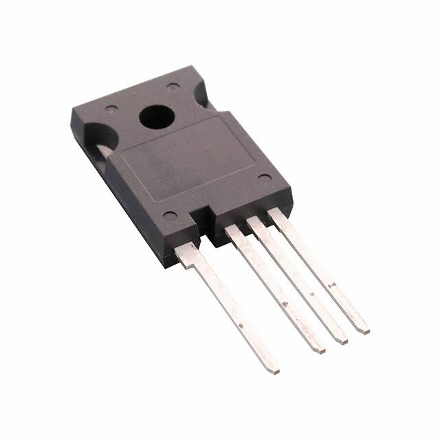
TO−247−4LD
CASE 340CJ
$Y
&Z
&3
&K
NVH4L040N65S3F
= ON Semiconductor Logo
= Assembly Plant Code
= Data Code (Year & Week)
= Lot
= Specific Device Code
ORDERING INFORMATION
Device
Package
Shipping
NVH4L040N65S3F TO−247−4LD 30 Units / Tube
(Pb−Free)
Publication Order Number:
NVH4L040N65S3F/D
�NVH4L040N65S3F
ELECTRICAL CHARACTERISTICS (TC = 25°C unless otherwise noted)
Parameter
Symbol
Test Conditions
Min
Typ
Max
Unit
OFF CHARACTERISTICS
Drain−to−Source Breakdown Voltage
BVDSS
VGS = 0 V, ID = 1 mA, TJ = 25°C
650
V
Drain−to−Source Breakdown Voltage
BVDSS
VGS = 0 V, ID = 10 mA, TJ = 150°C
700
V
Breakdown Voltage Temperature
Coefficient
DBVDSS/
DTJ
ID = 10 mA, Referenced to 25_C
Zero Gate Voltage Drain Current
IDSS
VGS = 0 V, VDS = 650 V
Gate−to−Body Leakage Current
IGSS
VGS = ±30 V, VDS = 0 V
VGS(th)
VGS = VDS, ID = 2.1 mA
DVGS(th)/DTJ
VGS = VDS, ID = 2.1 mA
−9
RDS(on)
VGS = 10 V, ID = 32.5 A
33.8
gFS
VDS = 20 V, ID = 32.5 A
40
S
5665
pF
640
mV/_C
10
mA
±100
nA
5.0
V
103
VDS = 520 V, TC = 125_C
ON CHARACTERISTICS
Gate Threshold Voltage
Threshold Temperature Coefficient
Static Drain−to−Source On Resistance
Forward Transconductance
3.0
mV/_C
40
mW
DYNAMIC CHARACTERISTICS
Input Capacitance
Ciss
Output Capacitance
Coss
VGS = 0 V, VDS = 400 V, f = 1 MHz
148
Reverse Transfer Capacitance
Crss
Effective Output Capacitance
Coss(eff.)
VDS = 0 V to 400 V, VGS = 0 V
1347
pF
Energy Related Output Capacitance
Coss(er.)
VDS = 0 V to 400 V, VGS = 0 V
240
pF
Total Gate Charge at 10 V
QG(TOT)
160
nC
Threshold Gate Charge
QG(TH)
VGS = 10 V, VDS = 400 V, ID = 32.5 A
(Note 6)
28.9
Gate−to−Source Gate Charge
QGS
Gate−to−Drain “Miller” Charge
QGD
Equivalent Series Resistance
ESR
15.8
47
65
f = 1 MHz
1.9
W
39
ns
27
ns
105
ns
7
ns
SWITCHING CHARACTERISTICS
Turn-On Delay Time
td(on)
Turn-On Rise Time
tr
Turn-Off Delay Time
td(off)
Turn-Off Fall Time
VGS = 10 V, VDD = 400 V,
ID = 32.5 A, Rg = 2.2 W
(Note 6)
tf
SOURCE−DRAIN DIODE CHARACTERISTICS
Maximum Continuous Source−to−
Drain Diode Forward Current
IS
Maximum Pulsed Source−to−Drain
Diode Forward Current
ISM
Source−to−Drain Diode Forward
Voltage
VSD
Reverse Recovery Time
trr
Charge Time
ta
Discharge Time
tb
Reverse Recovery Charge
Qrr
VGS = 0 V
VGS = 0 V
VGS = 0 V, ISD = 32.5 A
145.9
VGS = 0 V, dIF/dt = 100 A/ms,
ISD = 32.5 A
65
A
162.5
A
1.3
V
ns
117.3
28.8
744.5
nC
Product parametric performance is indicated in the Electrical Characteristics for the listed test conditions, unless otherwise noted. Product
performance may not be indicated by the Electrical Characteristics if operated under different conditions.
6. Essentially independent of operating temperature typical characteristics.
www.onsemi.com
2
�NVH4L040N65S3F
TYPICAL CHARACTERISTICS
10
5.5 V
1
200
1
10
Figure 2. On−Region Characteristics
4
5
6
7
8
9
0.06
TC = 25°C
0.05
VGS = 10 V
0.04
VGS = 20 V
0.03
0.02
0
CAPACITANCE (pF)
IS, REVERSE DRAIN CURRENT (A)
TJ = 25°C
0.01
0.5
150
180
Ciss
10K
1K
Coss
100
10
Crss
1
TJ = −55°C
0
120
100K
1
0.001
90
1M
TJ = 150°C
0.1
60
Figure 4. On−Resistance Variation vs. Drain
Current and Gate Voltage
250 ms Pulse Test
VGS = 0 V
10
30
ID, DRAIN CURRENT (A)
Figure 3. Transfer Characteristics
100
20
10
Figure 1. On−Region Characteristics
VGS, GATE−TO−SOURCE VOLTAGE (V)
1000
1
VDS, DRAIN−SOURCE VOLTAGE (V)
TJ = −55°C
3
0.1
VDS, DRAIN−SOURCE VOLTAGE (V)
TJ = 150°C
1
5.5 V
10
1
TJ = 25°C
10
7.0 V
6.0 V
20
250 ms Pulse Test
VDS = 20 V
100
VGS = 10 V
8.0 V
6.5 V
250 ms Pulse Test
TC = 25°C
0.2
250 ms Pulse Test
TC = 150°C
100
RDS(ON), DRAIN−SOURCE ON−RESISTANCE (W)
ID, DRAIN CURRENT (A)
7.0 V
6.5 V
6.0 V
0.1
ID, DRAIN CURRENT (A)
200
8.0 V
VGS = 10 V
ID, DRAIN CURRENT (A)
200
100
1.0
1.5
0.1
2.0
f = 1 MHz
VGS = 0 V
0.1
1
10
100
VSD, BODY DIODE FORWARD VOLTAGE (V)
VDS, DRAIN−TO−SOURCE VOLTAGE (V)
Figure 5. Body Diode Forward Voltage
Variation vs. Source Current and Temperature
Figure 6. Capacitance Characteristics
www.onsemi.com
3
1K
�NVH4L040N65S3F
VDD = 130 V
ID = 32.5 A
8
VDD = 400 V
6
4
2
0
0
60
120
180
1.2
VGS = 0 V
ID = 10 mA
1.1
1.0
0.9
0.8
−75
25
75
125
175
TJ, JUNCTION TEMPERATURE (°C)
Figure 7. Gate Charge Characteristics
Figure 8. Breakdown Voltage Variation vs.
Temperature
300
3.0
VGS = 10 V
ID = 32.5 A
2.0
1.5
1.0
0.5
0
−75
−25
25
75
125
10 ms
Operation in this Area
is Limited by RDS(ON)
DC
1
0.1
175
100 ms
1 ms
10
TC = 25°C
TJ = 150°C
Single Pulse
1
10
100
1K
TJ, JUNCTION TEMPERATURE (°C)
VDS, DRAIN−SOURCE VOLTAGE (V)
Figure 9. On−Resistance Variation vs.
Temperature
Figure 10. Maximum Safe Operating Area
80
40
70
35
60
30
50
25
40
30
20
15
20
10
10
5
25
30 ms
100
ID, DRAIN CURRENT (A)
2.5
0
−25
Qg, TOTAL GATE CHARGE (nC)
Eoss (mJ)
ID, DRAIN CURRENT (A)
RDS(ON), DRAIN−SOURCE ON−RESISTANCE (Normalized)
VGS, GATE−SOURCE VOLTAGE (V)
10
BVDSS, DRAIN−SOURCE
BREAKDOWN VOLTAGE (Normalized)
TYPICAL CHARACTERISTICS
50
75
100
125
0
150
0
130
260
390
520
650
TC, CASE TEMPERATURE (°C)
VDS, DRAIN−TO−SOURCE VOLTAGE (V)
Figure 11. Maximum Drain Current vs. Case
Temperature
Figure 12. EOSS vs. Drain−to−Source Voltage
www.onsemi.com
4
�NVH4L040N65S3F
1.2
200
NORMALIZED GATE THRESHOLD
VOLTAGE
RDS(ON), DRAIN−SOURCE ON−RESISTANCE (mW)
TYPICAL CHARACTERISTICS
180
160
140
120
100
TA = 150°C
80
60
Pulse Duration = 250 ms
Duty Cycle = 0.5% Max
ID = 32.5 A
40
20
0
4
5
6
TA = 25°C
7
8
9
VGS = VDS
ID = 2.1 mA
1.0
0.8
0.6
−80
10
−40
0
40
80
120
160
VGS, GATE−TO−SOURCE VOLTAGE (V)
TJ, JUNCTION TEMPERATURE (°C)
Figure 13. RDS(ON) vs. Gate Voltage
Figure 14. Normalized Gate Threshold Voltage
vs. Temperature
IAS, AVALANCHE CURRENT (A)
100
Starting TJ = 25°C
10
Starting TJ = 125°C
1
0.001
0.01
0.1
1
10
100
tAV, TIME IN AVALANCHE (ms)
r(t), NORMALIZED EFFECTIVE TRANSIENT
THERMAL RESISTANCE
Figure 15. Unclamped Inductive Switching
Capability
10
1
Duty Cycle = 0.5
0.2
0.1
0.1
0.05
0.02
PDM
0.01 0.01
0.001
t1
Single Pulse
0.00001
0.0001
0.001
t2
0.01
t, RECTANGULAR PULSE DURATION (s)
Figure 16. Transient Thermal Response Curve
www.onsemi.com
5
ZqJC(t) = r(t) x RqJC
RqJC = 0.28°C/W
Peak TJ = PDM x ZqJC(t) + TC
Duty Cycle, D = t1 / t2
0.1
1
�NVH4L040N65S3F
Figure 17. Gate Charge Test Circuit & Waveform
Figure 18. Resistive Switching Test Circuit & Waveforms
Figure 19. Unclamped Inductive Switching Test Circuit & Waveforms
www.onsemi.com
6
�NVH4L040N65S3F
Figure 20. Peak Diode Recovery dv/dt Test Circuit & Waveforms
SUPERFET and FRFET are registered trademarks of Semiconductor Components Industries, LLC (SCILLC) or its subsidiaries in the United States
and/or other countries.
www.onsemi.com
7
�NVH4L040N65S3F
PACKAGE DIMENSIONS
TO−247−4LD
CASE 340CJ
ISSUE A
www.onsemi.com
8
�NVH4L040N65S3F
ON Semiconductor and
are trademarks of Semiconductor Components Industries, LLC dba ON Semiconductor or its subsidiaries in the United States and/or other countries.
ON Semiconductor owns the rights to a number of patents, trademarks, copyrights, trade secrets, and other intellectual property. A listing of ON Semiconductor’s product/patent
coverage may be accessed at www.onsemi.com/site/pdf/Patent−Marking.pdf. ON Semiconductor reserves the right to make changes without further notice to any products herein.
ON Semiconductor makes no warranty, representation or guarantee regarding the suitability of its products for any particular purpose, nor does ON Semiconductor assume any liability
arising out of the application or use of any product or circuit, and specifically disclaims any and all liability, including without limitation special, consequential or incidental damages.
Buyer is responsible for its products and applications using ON Semiconductor products, including compliance with all laws, regulations and safety requirements or standards,
regardless of any support or applications information provided by ON Semiconductor. “Typical” parameters which may be provided in ON Semiconductor data sheets and/or
specifications can and do vary in different applications and actual performance may vary over time. All operating parameters, including “Typicals” must be validated for each customer
application by customer’s technical experts. ON Semiconductor does not convey any license under its patent rights nor the rights of others. ON Semiconductor products are not
designed, intended, or authorized for use as a critical component in life support systems or any FDA Class 3 medical devices or medical devices with a same or similar classification
in a foreign jurisdiction or any devices intended for implantation in the human body. Should Buyer purchase or use ON Semiconductor products for any such unintended or unauthorized
application, Buyer shall indemnify and hold ON Semiconductor and its officers, employees, subsidiaries, affiliates, and distributors harmless against all claims, costs, damages, and
expenses, and reasonable attorney fees arising out of, directly or indirectly, any claim of personal injury or death associated with such unintended or unauthorized use, even if such
claim alleges that ON Semiconductor was negligent regarding the design or manufacture of the part. ON Semiconductor is an Equal Opportunity/Affirmative Action Employer. This
literature is subject to all applicable copyright laws and is not for resale in any manner.
PUBLICATION ORDERING INFORMATION
LITERATURE FULFILLMENT:
Email Requests to: orderlit@onsemi.com
ON Semiconductor Website: www.onsemi.com
◊
TECHNICAL SUPPORT
North American Technical Support:
Voice Mail: 1 800−282−9855 Toll Free USA/Canada
Phone: 011 421 33 790 2910
www.onsemi.com
9
Europe, Middle East and Africa Technical Support:
Phone: 00421 33 790 2910
For additional information, please contact your local Sales Representative
�