Is Now Part of
To learn more about ON Semiconductor, please visit our website at
www.onsemi.com
Please note: As part of the Fairchild Semiconductor integration, some of the Fairchild orderable part numbers
will need to change in order to meet ON Semiconductor’s system requirements. Since the ON Semiconductor
product management systems do not have the ability to manage part nomenclature that utilizes an underscore
(_), the underscore (_) in the Fairchild part numbers will be changed to a dash (-). This document may contain
device numbers with an underscore (_). Please check the ON Semiconductor website to verify the updated
device numbers. The most current and up-to-date ordering information can be found at www.onsemi.com. Please
email any questions regarding the system integration to Fairchild_questions@onsemi.com.
ON Semiconductor and the ON Semiconductor logo are trademarks of Semiconductor Components Industries, LLC dba ON Semiconductor or its subsidiaries in the United States and/or other countries. ON Semiconductor owns the rights to a number
of patents, trademarks, copyrights, trade secrets, and other intellectual property. A listing of ON Semiconductor’s product/patent coverage may be accessed at www.onsemi.com/site/pdf/Patent-Marking.pdf. ON Semiconductor reserves the right
to make changes without further notice to any products herein. ON Semiconductor makes no warranty, representation or guarantee regarding the suitability of its products for any particular purpose, nor does ON Semiconductor assume any liability
arising out of the application or use of any product or circuit, and specifically disclaims any and all liability, including without limitation special, consequential or incidental damages. Buyer is responsible for its products and applications using ON
Semiconductor products, including compliance with all laws, regulations and safety requirements or standards, regardless of any support or applications information provided by ON Semiconductor. “Typical” parameters which may be provided in ON
Semiconductor data sheets and/or specifications can and do vary in different applications and actual performance may vary over time. All operating parameters, including “Typicals” must be validated for each customer application by customer’s
technical experts. ON Semiconductor does not convey any license under its patent rights nor the rights of others. ON Semiconductor products are not designed, intended, or authorized for use as a critical component in life support systems or any FDA
Class 3 medical devices or medical devices with a same or similar classification in a foreign jurisdiction or any devices intended for implantation in the human body. Should Buyer purchase or use ON Semiconductor products for any such unintended
or unauthorized application, Buyer shall indemnify and hold ON Semiconductor and its officers, employees, subsidiaries, affiliates, and distributors harmless against all claims, costs, damages, and expenses, and reasonable attorney fees arising out
of, directly or indirectly, any claim of personal injury or death associated with such unintended or unauthorized use, even if such claim alleges that ON Semiconductor was negligent regarding the design or manufacture of the part. ON Semiconductor
is an Equal Opportunity/Affirmative Action Employer. This literature is subject to all applicable copyright laws and is not for resale in any manner.
�NZT605
NPN Darlington Transistor
• This device designed for applications requiring extremely high gain at collector
currents to 1.0A and high breakdown voltage.
• Sourced from process 06.
4
3
2
1
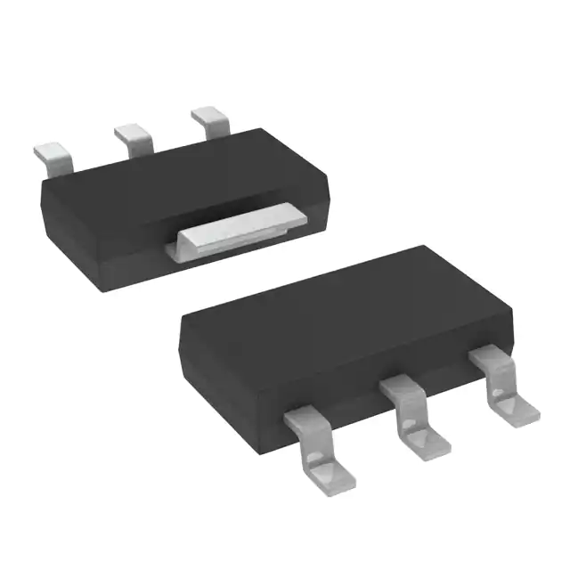
SOT-223
1. Base 2.4. Collector 3. Emitter
Absolute Maximum Ratings * T
C
Symbol
= 25°C unless otherwise noted
Parameter
Value
Units
VCEO
Collector-Emitter Voltage
110
V
VCBO
Collector-Base Voltage
140
V
VEBO
Emitter-Base Voltage
10
V
IC
Collector Current
TJ, TSTG
Operating and Storage Junction Temperature Range
- Continuous
1.5
A
-55 to +150
°C
* These ratings are limiting values above which the serviceability of any semiconductor device may be impaired.
NOTES:
1. These ratings are based on a maximum junction temperature of 150 degrees C.
2. These are steady limits. The factory should be consulted on application involving pulsed or low duty cycle operations
Electrical Characteristics *
Symbol
TC = 25°C unless otherwise noted
Parameter
Conditions
Min.
Max
Units
Off Characteristics
V(BR)CEO
Collector-Emitter Breakdown Voltage *
IC = 10mA, IB = 0
110
V
V(BR)CBO
Collector-Base Breakdown Voltage
IC = 100µA, IE = 0
140
V
V(BR)EBO
Emitter-Base Breakdown Voltage
IE = 100µA, IC = 0
10
ICBO
Collector Cutoff Current
VCB = 120V, IE = 0
ICES
Collector Cutoff Current
IEBO
Emitter Cut-off Current
V
10
nA
VCE = 120V, IE = 0
10
nA
VEB = 8.0V, IC = 0
100
nA
On Characteristics *
hFE
DC Current Gain
VCE = 5.0V, IC = 50mA
VCE = 5.0V, IC = 500mA
VCE = 5.0V, IC = 1.0A
VCE = 5.0V, IC = 1.5A
VCE = 5.0V, IC = 2.0A
2000
5000
2000
300
200
100K
VCE(sat)
Collector-Emitter Saturation Voltage
IC = 250mA, IB = 0.25mA
IC = 1.0A, IB = 1.0mA
1
1.5
V
VBE(sat)
Base-Emitter Saturation Voltage
IC = 1.0A, IB = 1.0mA
1.8
V
VBE(on)
Base-Emitter On Voltage
IC = 1.0A, VCE = 5.0V
1.7
V
Small Signal characteristics
fT
Transition Frequency
* Pulse Test: Pulse Width ≤ 300µs, Duty Cycle ≤ 2.0%
©2006 Fairchild Semiconductor Corporation
NZT605 Rev. C
IC = 100mA, VCE = 10V, f = 20MHz
1
150
MHz
www.fairchildsemi.com
NZT605 NPN Darlington Transistor
January 2007
�Ta = 25°C unless otherwise noted
Symbol
Parameter
PD
Total Device Dissipation
Derate above 25°C
RθJA
Thermal Resistance, Junction to Ambient
* Device mounted on FR-4PCB 36mm × 18mm × 1.5mm; mounting pad for the collector lead min.
2
NZT605 Rev. C
Max.
Units
1,000
8.0
mW
mW/°C
125
°C/W
6cm2
www.fairchildsemi.com
NZT605 NPN Darlington Transistor
Thermal Characteristics
�NZT605 NPN Darlington Transistor
Mechanical Dimensions
3.00 ±0.10
4.60 ±0.25
6.50 ±0.20
(0.89)
(0.95)
(0.46)
1.60 ±0.20
2.30 TYP
7.00 ±0.30
(0.60)
0.70 ±0.10
(0.95)
+0.04
0.06 –0.02
(0.60)
3.50 ±0.20
1.75 ±0.20
MAX1.80
0.65 ±0.20
0.08MAX
SOT-223
°
10
+0.10
0.25 –0.05
0°~
Dimensions in Millimeters
3
NZT605 Rev. C
www.fairchildsemi.com
�The following are registered and unregistered trademarks Fairchild Semiconductor owns or is authorized to use and is not intended to
be an exhaustive list of all such trademarks.
ACEx™
ActiveArray™
Bottomless™
Build it Now™
CoolFET™
CROSSVOLT™
DOME™
EcoSPARK™
E2CMOS™
EnSigna™
FACT®
FAST®
FASTr™
FPS™
FRFET™
FACT Quiet Series™
GlobalOptoisolator™
GTO™
HiSeC™
I2C™
i-Lo™
ImpliedDisconnect™
IntelliMAX™
ISOPLANAR™
LittleFET™
MICROCOUPLER™
MicroFET™
MicroPak™
MICROWIRE™
MSX™
MSXPro™
Across the board. Around the world.™
The Power Franchise®
Programmable Active Droop™
OCX™
OCXPro™
OPTOLOGIC®
OPTOPLANAR™
PACMAN™
POP™
Power247™
PowerEdge™
PowerSaver™
PowerTrench®
QFET®
QS™
QT Optoelectronics™
Quiet Series™
RapidConfigure™
RapidConnect™
µSerDes™
ScalarPump™
SILENT SWITCHER®
SMART START™
SPM™
Stealth™
SuperFET™
SuperSOT™-3
SuperSOT™-6
SuperSOT™-8
SyncFET™
TCM™
TinyBoost™
TinyBuck™
TinyPWM™
TinyPower™
TinyLogic®
TINYOPTO™
TruTranslation™
UHC®
UniFET™
VCX™
Wire™
DISCLAIMER
FAIRCHILD SEMICONDUCTOR RESERVES THE RIGHT TO MAKE CHANGES WITHOUT FURTHER NOTICE TO ANY PRODUCTS HEREIN TO
IMPROVE RELIABILITY, FUNCTION OR DESIGN. FAIRCHILD DOES NOT ASSUME ANY LIABILITY ARISING OUT OF THE APPLICATION OR USE
OF ANY PRODUCT OR CIRCUIT DESCRIBED HEREIN;NEITHER DOES IT CONVEY ANY LICENSE UNDER ITS PATENT RIGHTS, NOR THE
RIGHTS OF OTHERS. THESE SPECIFICATIONS DO NOT EXPAND THE TERMS OF FAIRCHILD’S WORLDWIDE TERMS AND CONDITIONS, SPECIFICALLY THE WARRANTY THEREIN, WHICH COVERS THESE PRODUCTS.
LIFE SUPPORT POLICY
FAIRCHILD’S PRODUCTS ARE NOT AUTHORIZED FOR USE AS CRITICAL COMPONENTS IN LIFE SUPPORT DEVICES OR SYSTEMS WITHOUT
THE EXPRESS WRITTEN APPROVAL OF FAIRCHILD SEMICONDUCTOR CORPORATION.
As used herein:
1. Life support devices or systems are devices or systems which, (a) are
intended for surgical implant into the body, or (b) support or sustain life, or
(c) whose failure to perform when properly used in accordance with
instructions for use provided in the labeling, can be reasonably expected
to result in significant injury to the user.
2. A critical component is any component of a life support device or system
whose failure to perform can be reasonably expected to cause the failure
of the life support device or system, or to affect its safety or effectiveness.
PRODUCT STATUS DEFINITIONS
Definition of Terms
Datasheet Identification
Product Status
Definition
Advance Information
Formative or In Design
This datasheet contains the design specifications for
product development. Specifications may change in
any manner without notice.
Preliminary
First Production
This datasheet contains preliminary data, and
supplementary data will be published at a later date.
Fairchild Semiconductor reserves the right to make
changes at any time without notice in order to improve
design.
No Identification Needed
Full Production
This datasheet contains final specifications. Fairchild
Semiconductor reserves the right to make changes at
any time without notice in order to improve design.
Obsolete
Not In Production
This datasheet contains specifications on a product
that has been discontinued by Fairchild semiconductor.
The datasheet is printed for reference information only.
Rev. I22
4
NZT605 Rev. C
www.fairchildsemi.com
NZT605 NPN Darlington Transistor
FAIRCHILD SEMICONDUCTOR TRADEMARKS
�ON Semiconductor and
are trademarks of Semiconductor Components Industries, LLC dba ON Semiconductor or its subsidiaries in the United States and/or other countries.
ON Semiconductor owns the rights to a number of patents, trademarks, copyrights, trade secrets, and other intellectual property. A listing of ON Semiconductor’s product/patent
coverage may be accessed at www.onsemi.com/site/pdf/Patent−Marking.pdf. ON Semiconductor reserves the right to make changes without further notice to any products herein.
ON Semiconductor makes no warranty, representation or guarantee regarding the suitability of its products for any particular purpose, nor does ON Semiconductor assume any liability
arising out of the application or use of any product or circuit, and specifically disclaims any and all liability, including without limitation special, consequential or incidental damages.
Buyer is responsible for its products and applications using ON Semiconductor products, including compliance with all laws, regulations and safety requirements or standards,
regardless of any support or applications information provided by ON Semiconductor. “Typical” parameters which may be provided in ON Semiconductor data sheets and/or
specifications can and do vary in different applications and actual performance may vary over time. All operating parameters, including “Typicals” must be validated for each customer
application by customer’s technical experts. ON Semiconductor does not convey any license under its patent rights nor the rights of others. ON Semiconductor products are not
designed, intended, or authorized for use as a critical component in life support systems or any FDA Class 3 medical devices or medical devices with a same or similar classification
in a foreign jurisdiction or any devices intended for implantation in the human body. Should Buyer purchase or use ON Semiconductor products for any such unintended or unauthorized
application, Buyer shall indemnify and hold ON Semiconductor and its officers, employees, subsidiaries, affiliates, and distributors harmless against all claims, costs, damages, and
expenses, and reasonable attorney fees arising out of, directly or indirectly, any claim of personal injury or death associated with such unintended or unauthorized use, even if such
claim alleges that ON Semiconductor was negligent regarding the design or manufacture of the part. ON Semiconductor is an Equal Opportunity/Affirmative Action Employer. This
literature is subject to all applicable copyright laws and is not for resale in any manner.
PUBLICATION ORDERING INFORMATION
LITERATURE FULFILLMENT:
Literature Distribution Center for ON Semiconductor
19521 E. 32nd Pkwy, Aurora, Colorado 80011 USA
Phone: 303−675−2175 or 800−344−3860 Toll Free USA/Canada
Fax: 303−675−2176 or 800−344−3867 Toll Free USA/Canada
Email: orderlit@onsemi.com
© Semiconductor Components Industries, LLC
N. American Technical Support: 800−282−9855 Toll Free
USA/Canada
Europe, Middle East and Africa Technical Support:
Phone: 421 33 790 2910
Japan Customer Focus Center
Phone: 81−3−5817−1050
www.onsemi.com
1
ON Semiconductor Website: www.onsemi.com
Order Literature: http://www.onsemi.com/orderlit
For additional information, please contact your local
Sales Representative
www.onsemi.com
�


 工商网监
湘ICP备2023018690号
工商网监
湘ICP备2023018690号