P3P8220A/AH
General Purpose Peak EMI
Reduction IC
Functional Description
P3P8220A/AH is a versatile, 1.8V/2.5V/3.3V Peak EMI reduction
IC. P3P8220A accepts an input clock from an external reference and
delivers a 1x modulated clock output.
P3P8220A is a Low drive part and P3P8220AH is a High drive part.
Refer to DC/AC Electrical characteristic table.
P3P8220A/AH operates with 1.8V/2.5V/3.3V supply and is
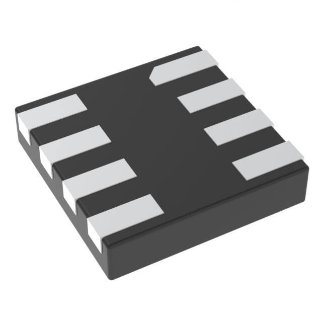
available in an 8 Pin, WDFN (2 mm x 2 mm) Package.
General Features
•
•
•
•
•
•
•
http://onsemi.com
MARKING
DIAGRAM
WDFN8
CASE 511AQ
1
1x, LVCMOS Peak EMI Reduction
Supports Non−continuous Input Clock Applications
Input / Output Frequency Range: Up to 60 MHz
Low and High Drive Part
Supply Voltage: 1.8 V±0.1 V
2.5 V±0.2 V
3.3 V±0.3 V
8−Pin, WDFN(2 mm x 2 mm) Package
These Devices are Pb−Free, Halogen Free/BFR Free and are RoHS
Compliant
Application
• P3P8220A is Targeted Towards Consumer Electronic Applications
VDD
1
GH MG
G
GH = Specific Device Code
M = Date Code
G
= Pb−Free Device
PIN CONFIGURATION
CLKIN 1
8
VDD
NC 2
7 NC
NC 3
6 NC
GND 4
5 ModOUT
ORDERING INFORMATION
See detailed ordering and shipping information in the package
dimensions section on page 6 of this data sheet.
CLKIN
Digital
Frequency
Modulation
ModOUT
GND
Figure 1. Block Diagram
© Semiconductor Components Industries, LLC, 2011
April, 2011 − Rev. 0
1
Publication Order Number:
P3P8220A/D
�P3P8220A/AH
Table 1. PIN DESCRIPTION
Pin #
Pin Name
Type
1
CLKIN
I
2
NC
No connection
3
NC
No connection
4
GND
P
Ground
5
ModOUT
O
Buffered Modulated Clock output.
6
NC
No connection
7
NC
No connection
8
VDD
P
Description
External reference Clock Input
1.8V/2.5V/3.3V Supply Voltage
Table 2. OPERATING CONDITIONS
Symbol
VDD
Description
Supply Voltage
1.8 V
2.5 V
3.3 V
Min
Max
Unit
1.7
2.3
3.0
1.9
2.7
3.6
V
0
70
°C
TA
Operating Temperature (Ambient Temperature)
CL
Load Capacitance
15
pF
CIN
Input Capacitance
7
pF
Table 3. ABSOLUTE MAXIMUM RATING
Symbol
VDD, VIN
TSTG
Description
Rating
Unit
Voltage on any input pin with respect to Ground
−0.5 to +4.6
V
Storage temperature
−65 to +125
°C
Ts
Max. Soldering Temperature (10 sec)
260
°C
TJ
Junction Temperature
150
°C
2
KV
TDV
Static Discharge Voltage (As per JEDEC STD22− A114−B)
Stresses exceeding Maximum Ratings may damage the device. Maximum Ratings are stress ratings only. Functional operation above the
Recommended Operating Conditions is not implied. Extended exposure to stresses above the Recommended Operating Conditions may
affect device reliability.
NOTE: These are stress ratings only and are not implied for functional use. Exposure to absolute maximum ratings for prolonged
periods of time may affect device reliability.
http://onsemi.com
2
�P3P8220A/AH
Table 4. ELECTRICAL CHARACTERISTICS
Symbol
Min
Typ
Max
Unit
1.7
1.8
1.9
V
VDD(2.5V)
2.3
2.5
2.7
VDD(3.3V)
3
3.3
3.6
VDD(1.8V)
Parameter
Test Conditions
Supply Voltage
VIL
Input LOW Voltage
VIH
Input HIGH Voltage
VOL
Output LOW Voltage
0.65*VDD
P3P8220A
VDD(1.8V), IOL = 4mA
0.35*VDD
V
VDD+0.3
V
0.25*VDD
V
VDD(2.5V, 3.3V), IOL = 8mA
P3P8220AH
VDD(1.8V), IOL = 6mA
VDD(2.5V, 3.3V), IOL = 12mA
VOH
Output HIGH Voltage
P3P8220A
VDD(1.8V), IOL = -4mA
0.75*VDD
V
VDD(2.5V, 3.3V), IOL = -8mA
P3P8220AH
VDD(1.8V), IOL =- 6mA
VDD(2.5V, 3.3V), IOL = -12mA
ICC
IDD
Static Supply Current
Dynamic Supply Current
CLKIN pulled LOW VDD(1.8V)
1.3
VDD(2.5V)
1.5
VDD(3.3V)
1.7
15 MHz
2.3
60 MHz
6.0
15 MHz
3.2
60 MHz
8.0
15 MHz
4.5
60 MHz
12
VDD(1.8V)
VDD(2.5V)
VDD(3.3V)
CL
Load Capacitance
Z0
Output Impedance
15
VDD(1.8V)
P3P8220A
50
P3P8220AH
30
VDD(2.5V)
P3P8220A
36
P3P8220AH
24
P3P8220A
30
P3P8220AH
20
VDD(3.3V)
http://onsemi.com
3
mA
mA
pF
W
�P3P8220A/AH
Table 5. SWITCHING CHARACTERISTICS
Max
Unit
Input Frequency
Parameter
60
MHz
ModOUT
60
Output Rise Time (Notes 1 & 2)
Test Conditions
Measured between 20% to 80%
VDD(1.8V)
VDD(2.5V)
VDD(3.3V)
Output Fall Time (Notes 1 & 2)
Measured between 20% to 80%
VDD(1.8V)
VDD(2.5V)
VDD(3.3V)
Output Duty Cycle (Notes 1, 2 & 3)
Measured at VDD/2
Cycle-to-Cycle Jitter (Note 1)
Unloaded spreaded output
VDD(1.8V)
VDD(3.3V)
Unloaded spreaded output
3.0
5.0
P3P8220AH
2.0
4.0
P3P8220A
1.8
3.0
P3P8220AH
1.2
2.5
P3P8220A
1.4
2.5
P3P8220AH
1.0
1.6
P3P8220A
2.4
4.0
P3P8220AH
1.6
3.0
P3P8220A
1.8
3.0
P3P8220AH
1.2
2.0
P3P8220A
1.4
2.0
P3P8220AH
1.0
1.6
50
55
15 MHz
±350
60 MHz
±200
15 MHz
±500
60 MHz
±150
15 MHz
±750
60 MHz
±200
7.5
VDD(2.5V)
7.5
VDD(3.3V)
7.5
http://onsemi.com
ns
%
ps
VDD(1.8V)
1. Parameter is guaranteed by design and characterization. Not 100% tested in production.
2. All parameters are specified with 15 pF loaded outputs.
3. For an input Duty Cycle (typ) of 50%.
4
Typ
P3P8220A
45
VDD(2.5V)
Maximum Input-Output Delay
(Notes 1 & 2)
Min
ns
�P3P8220A/AH
SWITCHING WAVEFORMS
t1
t2
VDD/2
VDD/2
VDD/2
OUTPUT
Figure 2. Duty Cycle Timing
80%
80%
20%
20%
OUTPUT
t3
t4
Figure 3. Output Rise/Fall Time
Figure 4. Input − Output Propagation Delay
VDDIN
C1
R
0.1 mF
Optional Noise
Reduction Filter
C2
2.2 mF
8
VDD
CLKIN
1 CLKIN
ModOUT 5
Rs
P3P8220A/AH
NC 2, 3, 6, 7
GND
4
NOTE:
Refer Pin Description table for Functionality details.
Figure 5. Typical Application Circuit
NOTE:
Device to Device variation of Tskew and I/O delay is $20%.
http://onsemi.com
5
ModOUT Cloc k
�P3P8220A/AH
ORDERING INFORMATION
Ordering Code
P3P8220AG−08CR
Marking
Temperature
Package Type
Shipping†
GH
0°C to +70°C
8−pin (2 mm x 2 mm) WDFN
(Pb−Free)
Tape & Reel
†For information on tape and reel specifications, including part orientation and tape sizes, please refer to our Tape and Reel Packaging
Specifications Brochure, BRD8011/D.
*A “microdot” placed at the end of last row of marking or just below the last row toward the center of package indicates Pb−Free.
http://onsemi.com
6
�P3P8220A/AH
PACKAGE DIMENSIONS
WDFN8 2x2, 0.5P
CASE 511AQ−01
ISSUE A
D
PIN ONE
REFERENCE
2X
A
B
L1
ÍÍÍ
ÍÍÍ
ÍÍÍ
DETAIL A
E
OPTIONAL
CONSTRUCTIONS
0.10 C
2X
0.10 C
ÉÉ
ÉÉ
TOP VIEW
EXPOSED Cu
A3
DETAIL B
0.05 C
0.05 C
MOLD CMPD
OPTIONAL
CONSTRUCTION
C
MILLIMETERS
MIN
MAX
0.80
0.70
0.05
0.00
0.20 REF
0.20
0.30
2.00 BSC
2.00 BSC
0.50 BSC
0.50
0.60
--0.15
RECOMMENDED
SOLDERING FOOTPRINT*
A1
SIDE VIEW
DIM
A
A1
A3
b
D
E
e
L
L1
DETAIL B
A
8X
SEATING
PLANE
7X
0.78
PACKAGE
OUTLINE
DETAIL A
1
NOTES:
1. DIMENSIONING AND TOLERANCING PER
ASME Y14.5M, 1994.
2. CONTROLLING DIMENSION: MILLIMETERS.
3. DIMENSION b APPLIES TO PLATED
TERMINAL AND IS MEASURED BETWEEN
0.15 AND 0.30mm FROM TERMINAL.
L
L
8X
4
L
2.30
0.88
8
5
e/2
e
8X
b
0.10 C A
0.05 C
8X
1
0.35
B
0.50
PITCH
DIMENSIONS: MILLIMETERS
NOTE 3
*For additional information on our Pb−Free strategy and soldering
details, please download the ON Semiconductor Soldering and
Mounting Techniques Reference Manual, SOLDERRM/D.
BOTTOM VIEW
ON Semiconductor and
are registered trademarks of Semiconductor Components Industries, LLC (SCILLC). SCILLC reserves the right to make changes without further notice
to any products herein. SCILLC makes no warranty, representation or guarantee regarding the suitability of its products for any particular purpose, nor does SCILLC assume any liability
arising out of the application or use of any product or circuit, and specifically disclaims any and all liability, including without limitation special, consequential or incidental damages.
“Typical” parameters which may be provided in SCILLC data sheets and/or specifications can and do vary in different applications and actual performance may vary over time. All
operating parameters, including “Typicals” must be validated for each customer application by customer’s technical experts. SCILLC does not convey any license under its patent rights
nor the rights of others. SCILLC products are not designed, intended, or authorized for use as components in systems intended for surgical implant into the body, or other applications
intended to support or sustain life, or for any other application in which the failure of the SCILLC product could create a situation where personal injury or death may occur. Should
Buyer purchase or use SCILLC products for any such unintended or unauthorized application, Buyer shall indemnify and hold SCILLC and its officers, employees, subsidiaries, affiliates,
and distributors harmless against all claims, costs, damages, and expenses, and reasonable attorney fees arising out of, directly or indirectly, any claim of personal injury or death
associated with such unintended or unauthorized use, even if such claim alleges that SCILLC was negligent regarding the design or manufacture of the part. SCILLC is an Equal
Opportunity/Affirmative Action Employer. This literature is subject to all applicable copyright laws and is not for resale in any manner.
PUBLICATION ORDERING INFORMATION
LITERATURE FULFILLMENT:
Literature Distribution Center for ON Semiconductor
P.O. Box 5163, Denver, Colorado 80217 USA
Phone: 303−675−2175 or 800−344−3860 Toll Free USA/Canada
Fax: 303−675−2176 or 800−344−3867 Toll Free USA/Canada
Email: orderlit@onsemi.com
N. American Technical Support: 800−282−9855 Toll Free
USA/Canada
Europe, Middle East and Africa Technical Support:
Phone: 421 33 790 2910
Japan Customer Focus Center
Phone: 81−3−5773−3850
http://onsemi.com
7
ON Semiconductor Website: www.onsemi.com
Order Literature: http://www.onsemi.com/orderlit
For additional information, please contact your local
Sales Representative
P3P8220A/D
�