ON Semiconductor
Is Now
To learn more about onsemi™, please visit our website at
www.onsemi.com
onsemi and and other names, marks, and brands are registered and/or common law trademarks of Semiconductor Components Industries, LLC dba “onsemi” or its affiliates and/or
subsidiaries in the United States and/or other countries. onsemi owns the rights to a number of patents, trademarks, copyrights, trade secrets, and other intellectual property. A listing of onsemi
product/patent coverage may be accessed at www.onsemi.com/site/pdf/Patent-Marking.pdf. onsemi reserves the right to make changes at any time to any products or information herein, without
notice. The information herein is provided “as-is” and onsemi makes no warranty, representation or guarantee regarding the accuracy of the information, product features, availability, functionality,
or suitability of its products for any particular purpose, nor does onsemi assume any liability arising out of the application or use of any product or circuit, and specifically disclaims any and all
liability, including without limitation special, consequential or incidental damages. Buyer is responsible for its products and applications using onsemi products, including compliance with all laws,
regulations and safety requirements or standards, regardless of any support or applications information provided by onsemi. “Typical” parameters which may be provided in onsemi data sheets and/
or specifications can and do vary in different applications and actual performance may vary over time. All operating parameters, including “Typicals” must be validated for each customer application
by customer’s technical experts. onsemi does not convey any license under any of its intellectual property rights nor the rights of others. onsemi products are not designed, intended, or authorized
for use as a critical component in life support systems or any FDA Class 3 medical devices or medical devices with a same or similar classification in a foreign jurisdiction or any devices intended for
implantation in the human body. Should Buyer purchase or use onsemi products for any such unintended or unauthorized application, Buyer shall indemnify and hold onsemi and its officers, employees,
subsidiaries, affiliates, and distributors harmless against all claims, costs, damages, and expenses, and reasonable attorney fees arising out of, directly or indirectly, any claim of personal injury or death
associated with such unintended or unauthorized use, even if such claim alleges that onsemi was negligent regarding the design or manufacture of the part. onsemi is an Equal Opportunity/Affirmative
Action Employer. This literature is subject to all applicable copyright laws and is not for resale in any manner. Other names and brands may be claimed as the property of others.
�Features
Description
■ λ = 880nm
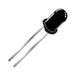
The QED223 is 880nm AlGaAs LEDs encapsulated
in a clear purple tinted, plastic T-1 3/4 package.
■ Chip material = AlGaAs
■ Package type: T-1 3/4 (5mm lens diameter)
■ Matched photosensor: QSD123/QSD124
■ Medium wide emission angle, 30°
■ High output power
■ Package material and color: clear, purple tinted, plastic
Package Dimensions
0.195 (4.95)
REFERENCE
SURFACE
0.305 (7.75)
0.040 (1.02)
NOM
0.800 (20.3)
MIN
CATHODE
0.050
(1.25)
Schematic
0.100 (2.54)
NOM
ANODE
0.240 (6.10)
0.215 (5.45)
CATHODE
0.020 (0.51)
SQ. (2X)
Notes:
1. Dimensions of all drawings are in inches (mm).
2. Tolerance is ±0.010 (0.25) on all non-nominal dimensions
unless otherwise specified.
©2001 Semiconductor Components Industries, LLC.
October-2017, Rev. 3
Publication Order Number:
QED223/D
QED223 — Plastic Infrared Light Emitting Diode
QED223
Plastic Infrared Light Emitting Diode
�Stresses exceeding the absolute maximum ratings may damage the device. The device may not function or be
operable above the recommended operating conditions and stressing the parts to these levels is not recommended.
In addition, extended exposure to stresses above the recommended operating conditions may affect device reliability.
The absolute maximum ratings are stress ratings only.
Symbol
Parameter
TOPR
Operating Temperature
Rating
Units
-40 to +100
°C
TSTG
Storage Temperature
-40 to +100
°C
TSOL-I
Soldering Temperature (Iron)(2)(3)(4)
240 for 5 sec
°C
TSOL-F
Soldering Temperature (Flow)(2)(3)
260 for 10 sec
°C
100
mA
IF
Continuous Forward Current
VR
Reverse Voltage
5
V
PD
Power Dissipation(1)
200
mW
Peak Forward Current(5)
1.5
A
IF(Peak)
Notes:
1. Derate power dissipation linearly 2.67mW/°C above 25°C.
2. RMA flux is recommended.
3. Methanol or isopropyl alcohols are recommended as cleaning agents.
4. Soldering iron 1/16" (1.6mm) minimum from housing.
5. Pulse conditions; tp = 100µs, T = 10ms.
Electrical / Optical Characteristics (TA = 25°C)
Symbol
Parameter
λPE
Peak Emission Wavelength
TCλ
Temperature Coefficient
Test Conditions
IF = 20mA
2Θ1/2
Emission Angle
IF = 100mA
VF
Forward Voltage
IF = 100mA, tp = 20ms
TCVF
VR = 5V
IE
Radiant Intensity
IF = 100mA, tp = 20ms
Temperature Coefficient
Rise Time
tf
Fall Time
Cj
Junction Capacitance
Max.
IF = 100mA
VR = 0V
www.onsemi.com
2
Units
890
nm
0.2
nm / °C
30
°
-6
Reverse Current
tr
Typ.
1.7
Temperature Coefficient
IR
TCIE
Min.
V
mV / °C
10
µA
mW/sr
25
-0.3
% / °C
900
ns
800
ns
11
pF
QED223 — Plastic Infrared Light Emitting Diode
Absolute Maximum Ratings (TA = 25°C unless otherwise specified)
�Figure 1. Normalized Intensity vs. Wavelength
Figure 2. Peak Wavelength vs. Ambient Temperature
1.0
λPE – PEAK EMISSION WAVELENGTH
910
NORMALIZED INTENSITY
0.9
0.8
0.7
0.6
0.5
0.4
0.3
0.2
0.1
0.0
700
750
800
850
900
950
1,000
IF = 20mA DC
908
906
904
902
900
898
896
894
1,050
0
10
20
λ (nm)
Ie – NORMALIZED RADIANT INTENSITY
Ie – NORMALIZED RADIANT INTENSITY
50
60
1.3
Normalized to:
IF = 100mA Pulsed
tPW = 20ms
Duty Cycle = 4%
TA = 25°C
1
0.1
10
100
80
70
90
100
Normalized to:
IF = 20mA Pulsed
tPW = 20ms
Duty Cycle = 4%
TA = 25°C
1.2
1.1
1.0
0.9
0.8
0.7
0.6
-15
1000
0
15
30
45
60
75
90
105
TA – AMBIENT TEMPERTURE (°C)
IF – FORWARD CURRENT (mA)
Figure 6. Forward Voltage vs. Ambient Temperature
Figure 5. Forward Voltage vs. Forward Current
5.0
2.1
IF Pulsed
tPW = 20ms
Duty Cycle = 4%
TA = 25°C
VF – FORWARD VOLTAGE (V)
VF – FORWARD VOLTAGE (V)
40
Figure 4. Normalized Radient Intensity vs. Ambient Temperature
Figure 3. Normalized Radiant Intensity vs. Forward Current
10
4.0
30
TA – AMBIENT TEMPERTURE (°C)
3.0
2.0
1.0
IF = 20mA Pulsed
tPW = 20ms
Duty Cycle = 4%
2.0
1.9
1.8
1.7
1.6
0.0
1.5
10
100
1000
-15
0
15
30
45
60
75
TA – AMBIENT TEMPERTURE (°C)
IF – FORWARD CURRENT (mA)
www.onsemi.com
3
90
105
QED223 — Plastic Infrared Light Emitting Diode
Typical Performance Curves
�110°
100°
90°
80°
70°
120°
60°
130°
50°
140°
40°
150°
30°
160°
20°
170°
10°
180°
1.0
0.8
0.6
0.4
0.2
0.0
0.2
0.4
0.6
0.8
0°
1.0
IC (ON) – NORMALIZED COLLECTOR CURRENT
Figure 8. Coupling Characteristics of QED22X and QSD22X
Figure 7. Radiation Diagram
1.0
Normalized to:
d = 0 inch
Pulse Width = 100μs
Duty Cycle = 0.1%
VCC = 5V
RL = 100Ω
TA = 25°C
0.8
0.6
IF = 100mA
0.4
IF = 20mA
0.2
0.0
0
1
2
3
4
LENS TIP SEPARATION (inches)
www.onsemi.com
4
5
6
QED223 — Plastic Infrared Light Emitting Diode
Typical Performance Curves (Continued)
�ON Semiconductor and
are trademarks of Semiconductor Components Industries, LLC dba ON Semiconductor or its subsidiaries in the United States and/or other countries.
ON Semiconductor owns the rights to a number of patents, trademarks, copyrights, trade secrets, and other intellectual property. A listing of ON Semiconductor’s product/patent
coverage may be accessed at www.onsemi.com/site/pdf/Patent−Marking.pdf. ON Semiconductor reserves the right to make changes without further notice to any products herein.
ON Semiconductor makes no warranty, representation or guarantee regarding the suitability of its products for any particular purpose, nor does ON Semiconductor assume any liability
arising out of the application or use of any product or circuit, and specifically disclaims any and all liability, including without limitation special, consequential or incidental damages.
Buyer is responsible for its products and applications using ON Semiconductor products, including compliance with all laws, regulations and safety requirements or standards,
regardless of any support or applications information provided by ON Semiconductor. “Typical” parameters which may be provided in ON Semiconductor data sheets and/or
specifications can and do vary in different applications and actual performance may vary over time. All operating parameters, including “Typicals” must be validated for each customer
application by customer’s technical experts. ON Semiconductor does not convey any license under its patent rights nor the rights of others. ON Semiconductor products are not
designed, intended, or authorized for use as a critical component in life support systems or any FDA Class 3 medical devices or medical devices with a same or similar classification
in a foreign jurisdiction or any devices intended for implantation in the human body. Should Buyer purchase or use ON Semiconductor products for any such unintended or unauthorized
application, Buyer shall indemnify and hold ON Semiconductor and its officers, employees, subsidiaries, affiliates, and distributors harmless against all claims, costs, damages, and
expenses, and reasonable attorney fees arising out of, directly or indirectly, any claim of personal injury or death associated with such unintended or unauthorized use, even if such
claim alleges that ON Semiconductor was negligent regarding the design or manufacture of the part. ON Semiconductor is an Equal Opportunity/Affirmative Action Employer. This
literature is subject to all applicable copyright laws and is not for resale in any manner.
PUBLICATION ORDERING INFORMATION
LITERATURE FULFILLMENT:
Literature Distribution Center for ON Semiconductor
19521 E. 32nd Pkwy, Aurora, Colorado 80011 USA
Phone: 303−675−2175 or 800−344−3860 Toll Free USA/Canada
Fax: 303−675−2176 or 800−344−3867 Toll Free USA/Canada
Email: orderlit@onsemi.com
❖
© Semiconductor Components Industries, LLC
N. American Technical Support: 800−282−9855 Toll Free
USA/Canada
Europe, Middle East and Africa Technical Support:
Phone: 421 33 790 2910
Japan Customer Focus Center
Phone: 81−3−5817−1050
ON Semiconductor Website: www.onsemi.com
Order Literature: http://www.onsemi.com/orderlit
For additional information, please contact your local
Sales Representative
www.onsemi.com
�