Is Now Part of
To learn more about ON Semiconductor, please visit our website at
www.onsemi.com
Please note: As part of the Fairchild Semiconductor integration, some of the Fairchild orderable part numbers
will need to change in order to meet ON Semiconductor’s system requirements. Since the ON Semiconductor
product management systems do not have the ability to manage part nomenclature that utilizes an underscore
(_), the underscore (_) in the Fairchild part numbers will be changed to a dash (-). This document may contain
device numbers with an underscore (_). Please check the ON Semiconductor website to verify the updated
device numbers. The most current and up-to-date ordering information can be found at www.onsemi.com. Please
email any questions regarding the system integration to Fairchild_questions@onsemi.com.
ON Semiconductor and the ON Semiconductor logo are trademarks of Semiconductor Components Industries, LLC dba ON Semiconductor or its subsidiaries in the United States and/or other countries. ON Semiconductor owns the rights to a number
of patents, trademarks, copyrights, trade secrets, and other intellectual property. A listing of ON Semiconductor’s product/patent coverage may be accessed at www.onsemi.com/site/pdf/Patent-Marking.pdf. ON Semiconductor reserves the right
to make changes without further notice to any products herein. ON Semiconductor makes no warranty, representation or guarantee regarding the suitability of its products for any particular purpose, nor does ON Semiconductor assume any liability
arising out of the application or use of any product or circuit, and specifically disclaims any and all liability, including without limitation special, consequential or incidental damages. Buyer is responsible for its products and applications using ON
Semiconductor products, including compliance with all laws, regulations and safety requirements or standards, regardless of any support or applications information provided by ON Semiconductor. “Typical” parameters which may be provided in ON
Semiconductor data sheets and/or specifications can and do vary in different applications and actual performance may vary over time. All operating parameters, including “Typicals” must be validated for each customer application by customer’s
technical experts. ON Semiconductor does not convey any license under its patent rights nor the rights of others. ON Semiconductor products are not designed, intended, or authorized for use as a critical component in life support systems or any FDA
Class 3 medical devices or medical devices with a same or similar classification in a foreign jurisdiction or any devices intended for implantation in the human body. Should Buyer purchase or use ON Semiconductor products for any such unintended
or unauthorized application, Buyer shall indemnify and hold ON Semiconductor and its officers, employees, subsidiaries, affiliates, and distributors harmless against all claims, costs, damages, and expenses, and reasonable attorney fees arising out
of, directly or indirectly, any claim of personal injury or death associated with such unintended or unauthorized use, even if such claim alleges that ON Semiconductor was negligent regarding the design or manufacture of the part. ON Semiconductor
is an Equal Opportunity/Affirmative Action Employer. This literature is subject to all applicable copyright laws and is not for resale in any manner.
�RHRP3060
30 A, 600 V Hyperfast Diodes
Features
Description
• Hyperfast Recovery trr = 45 ns (@ IF = 30 A)
The RHRP3060 is a hyperfast diode with soft recovery
characteristics. It has the half recovery time of ultrafast
diodes and is silicon nitride passivated ionimplanted
epitaxial planar construction. These devices are intended to
be used as freewheeling clamping diodes and diodes in a
variety of switching power supplies and other power
switching applications. Their low stored charge and
hyperfast soft recovery minimize ringing and electrical noise
in many power switching circuits reducing power loss in the
switching transistors.
• Max Forward Voltage, VF = 2.1 V (@ TC = 25°C)
• 600 V Reverse Voltage and High Reliability
• Avalanche Energy Rated
• RoHS Compliant
Applications
• Switching Power Supplies
• Power Switching Circuits
• General Purpose
Ordering Informations
Part Number
Package
Brand
RHRP3060
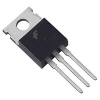
TO-220AC-2L
RHRP3060
Pin Assignments
1. Cathode
TO-220
2. Anode
Absolute Maximum Ratings
Symbol
Parameter
RHRP3060
Unit
VRRM
Peak Repetitive Reverse Voltage
600
V
VRWM
Working Peak Reverse Voltage
600
V
VR
DC Blocking Voltage
600
V
IF(AV)
Average Rectified Forward Current (TC = 120C)
30
A
IFRM
Repetitive Peak Surge Current (Square Wave, 20KHz)
70
A
IFSM
Nonrepetitive Peak Surge Current
(Halfwave, 1 Phase, 60Hz)
325
A
PD
Maximum Power Dissipation
125
W
EAVL
Avalanche Energy (See Figures 10 and 11)
20
mJ
TJ, TSTG
Operating and Storage Temperature
-65 to 175
C
©2005 Fairchild Semiconductor Corporation
RHRP3060 Rev. C
1
www.fairchildsemi.com
RHRP3060 — Hyperfast Diode
November 2013
�Symbol
VF
IR
TC = 25°C unless otherwise noted
Test Conditions
RHRP3060
Min.
Typ.
Max.
Unit
IF = 30 A
-
-
2.1
V
IF = 30 A, TC = 150C
-
-
1.7
V
VR = 400 V
-
-
-
A
VR = 600 V
-
-
250
A
VR = 400 V, TC = 150C
-
-
-
mA
VR = 600 V, TC = 150C
-
-
1.0
mA
IF = 1 A, dlF/dt = 200 A/s
-
-
40
ns
IF = 30 A, dlF/dt = 200 A/s
-
-
45
ns
ta
IF = 30 A, dlF/dt = 200 A/s
-
22
-
ns
tb
IF = 30 A, dlF/dt = 200 A/s
-
18
-
ns
QRR
IF = 30 A, dlF/dt = 200 A/s
-
100
-
nC
CJ
VR = 600 V, IF = 0 A
-
85
-
pF
-
-
1.2
C/W
trr
RJC
DEFINITIONS
VF = Instantaneous forward voltage (pw = 300s, D = 2%)
IR = Instantaneous reverse current.
trr = Reverse recovery time (See Figure 9), summation of ta + tb.
ta = Time to reach peak reverse current (See Figure 9).
tb = Time from peak IRM to projected zero crossing of IRM based on a straight line from peak IRM through 25% of IRM (See Figure 9).
QRR = Reverse recovery charge.
CJ = Junction Capacitance.
RJC = Thermal resistance junction to case.
pw = pulse width.
D = Duty cycle.
©2005 Fairchild Semiconductor Corporation
RHRP3060 Rev. C
2
www.fairchildsemi.com
RHRP3060 — Hyperfast Diode
Electrical Characteristics
�Figure 1. Forward Current vs Forward Voltage
Figure 2. Reverse Currnt vs Reverse Voltage
2000
IR , REVERSE CURRENT (μA)
IF , FORWARD CURRENT (A)
300
100
100C
25oC
175C
10
1
0
1
2
3
175C
100
100C
10
1
0.1
25C
0.01
4
0
200
100
VF , FORWARD VOLTAGE (V)
Figure 3. trr, ta and tb Curves vs
Forward Current
100
40
t, RECOVERY TIMES (ns)
t, RECOVERY TIMES (ns)
TC = 25C, dlF/dt = 200A/s
trr
20
ta
10
tb
500
600
TC = 100C, dlF/dt = 200A/s
80
trr
60
40
ta
tb
20
0
0
10
1
30
10
IF , FORWARD CURRENT (A)
1
IF , FORWARD CURRENT (A)
150
TC = 175C, dlF/dt = 200A/s
125
trr
100
75
ta
50
tb
25
0
10
1
RHRP3060 Rev. C
30
25
DC
20
SQ.WAVE
15
10
5
0
75
30
100
125
150
175
TC , CASE TEMPERATURE (oC)
IF , FORWARD CURRENT (A)
©2005 Fairchild Semiconductor Corporation
30
Figure 6. Current Derating Curve
IF(AV) , AVERAGE FORWARD CURRENT (A)
Figure 5. trr, ta and tb Curves vs
Forward Current
t, RECOVERY TIMES (ns)
400
Figure 4. trr, ta and tb Curves vs
Forward Current
50
30
300
VR , REVERSE VOLTAGE (V)
3
www.fairchildsemi.com
RHRP3060 — Hyperfast Diode
Typical Performance Characteristics
�RHRP3060 — Hyperfast Diode
Typical Performance Characteristics
(Continued)
Figure 7. Junction Capacitance vs
Reverse Voltage
CJ , JUNCTION CAPACITANCE (pF)
150
125
100
75
50
25
0
0
50
150
100
200
VR , REVERSE VOLTAGE (V)
Test Circuit and Waveforms
Figure 8. trr Test Circuit
VGE AMPLITUDE AND
RG CONTROL dIF/dt
t1 AND t2 CONTROL IF
L
DUT
RG
VGE
Figure 9. trr Waveforms and Definitions
CURRENT
SENSE
-
dIF
trr
dt
ta
tb
0
+
IGBT
t1
IF
VDD
0.25 IRM
IRM
t2
Figure 10. Avalanche Energy Test Circuit
Figure 11. Avalanche Current and Voltage
Waveforms
I = 1A
L = 40mH
R < 0.1Ω
EAVL = 1/2LI2 [VR(AVL) /(VR(AVL) - VDD)]
Q1 = IGBT (BVCES > DUT VR(AVL))
VAVL
L
CURRENT
SENSE
R
IL
IL
+
VDD
I V
Q1
VDD
DUT
©2005 Fairchild Semiconductor Corporation
RHRP3060 Rev. C
t0
-
4
t1
t2
t
www.fairchildsemi.com
�4.09
3.50
0.36 M
10.67
9.65
A
B A M
B
3.43
2.54
8.89
6.86
1.40
0.51
7°
3°
6.86
5.84
16.51
14.22
9.40
8.38
5°
3°
1
2
5°
3°
16.15
15.75
13.40
12.19
6.35 MAX
0.60 MAX
C
1.65
1.25
1.91
14.73
13.60
0.61
0.33
2.54
2.92
2.03
1.02
0.38
5.08
5°
3°
0.36 M
C A B
5°
3°
4.80
4.30
NOTES:
A. PACKAGE REFERENCE: JEDEC TO220,ISSUE K,
VARIATION AC,DATED APRIL 2002.
B. ALL DIMENSIONS ARE IN MILLIMETERS.
C. DIMENSION AND TOLERANCE AS PER ASME
Y14.5-2009.
D. DIMENSIONS ARE EXCLUSIVE OF BURRS,
MOLD FLASH AND TIE BAR PROTRUSIONS.
E. DRAWING FILE NAME: TO220A02REV5
�ON Semiconductor and
are trademarks of Semiconductor Components Industries, LLC dba ON Semiconductor or its subsidiaries in the United States and/or other countries.
ON Semiconductor owns the rights to a number of patents, trademarks, copyrights, trade secrets, and other intellectual property. A listing of ON Semiconductor’s product/patent
coverage may be accessed at www.onsemi.com/site/pdf/Patent−Marking.pdf. ON Semiconductor reserves the right to make changes without further notice to any products herein.
ON Semiconductor makes no warranty, representation or guarantee regarding the suitability of its products for any particular purpose, nor does ON Semiconductor assume any liability
arising out of the application or use of any product or circuit, and specifically disclaims any and all liability, including without limitation special, consequential or incidental damages.
Buyer is responsible for its products and applications using ON Semiconductor products, including compliance with all laws, regulations and safety requirements or standards,
regardless of any support or applications information provided by ON Semiconductor. “Typical” parameters which may be provided in ON Semiconductor data sheets and/or
specifications can and do vary in different applications and actual performance may vary over time. All operating parameters, including “Typicals” must be validated for each customer
application by customer’s technical experts. ON Semiconductor does not convey any license under its patent rights nor the rights of others. ON Semiconductor products are not
designed, intended, or authorized for use as a critical component in life support systems or any FDA Class 3 medical devices or medical devices with a same or similar classification
in a foreign jurisdiction or any devices intended for implantation in the human body. Should Buyer purchase or use ON Semiconductor products for any such unintended or unauthorized
application, Buyer shall indemnify and hold ON Semiconductor and its officers, employees, subsidiaries, affiliates, and distributors harmless against all claims, costs, damages, and
expenses, and reasonable attorney fees arising out of, directly or indirectly, any claim of personal injury or death associated with such unintended or unauthorized use, even if such
claim alleges that ON Semiconductor was negligent regarding the design or manufacture of the part. ON Semiconductor is an Equal Opportunity/Affirmative Action Employer. This
literature is subject to all applicable copyright laws and is not for resale in any manner.
PUBLICATION ORDERING INFORMATION
LITERATURE FULFILLMENT:
Literature Distribution Center for ON Semiconductor
19521 E. 32nd Pkwy, Aurora, Colorado 80011 USA
Phone: 303−675−2175 or 800−344−3860 Toll Free USA/Canada
Fax: 303−675−2176 or 800−344−3867 Toll Free USA/Canada
Email: orderlit@onsemi.com
© Semiconductor Components Industries, LLC
N. American Technical Support: 800−282−9855 Toll Free
USA/Canada
Europe, Middle East and Africa Technical Support:
Phone: 421 33 790 2910
Japan Customer Focus Center
Phone: 81−3−5817−1050
www.onsemi.com
1
ON Semiconductor Website: www.onsemi.com
Order Literature: http://www.onsemi.com/orderlit
For additional information, please contact your local
Sales Representative
www.onsemi.com
�