Ordering number : ENA1742A
SFT1446
N-Channel Power MOSFET
http://onsemi.com
60V, 20A, 51mΩ, Single TP/TP-FA
Features
•
•
•
ON-resistance RDS(on)1=39mΩ(typ.)
4V drive
Protection diode in
•
•
Input Capacitance Ciss=750pF(typ.)
Halogen free compliance
Specifications
Absolute Maximum Ratings at Ta=25°C
Parameter
Symbol
Drain-to-Source Voltage
Conditions
Ratings
Unit
VDSS
VGSS
Gate-to-Source Voltage
Drain Current (DC)
ID
IDP
Drain Current (Pulse)
60
PW≤10μs, duty cycle≤1%
V
±20
V
20
A
80
A
1
W
Allowable Power Dissipation
PD
23
W
Channel Temperature
Tch
150
°C
Storage Temperature
Tstg
--55 to +150
°C
Tc=25°C
Stresses exceeding Maximum Ratings may damage the device. Maximum Ratings are stress ratings only. Functional operation above the Recommended Operating
Conditions is not implied. Extended exposure to stresses above the Recommended Operating Conditions may affect device reliability.
Package Dimensions
Package Dimensions
unit : mm (typ)
7518-004
unit : mm (typ)
7003-004
0.5
1.5
5.5
0.5
1
2
2.3
0.8
1.2
7.5
0.8
1.6
0.6
1
2.3
2
3
0 to 0.2
0.6
0.5
3
2.5
0.85
0.85
0.7
1 : Gate
2 : Drain
3 : Source
4 : Drain
1.2
2.3
2.3
1 : Gate
2 : Drain
3 : Source
4 : Drain
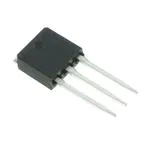
TP-FA
TP
Product & Package Information
Product & Package Information
• Package : TP
• JEITA, JEDEC : SC-64, TO-251
• Minimum Packing Quantity : 500 pcs./bag
• Package : TP-FA
• JEITA, JEDEC : SC-63, TO-252
• Minimum Packing Quantity : 700 pcs./reel
Marking(TP, TP-FA)
SFT1446-TL-H
1.2
1.5
4
7.0
5.5
4
2.3
6.5
5.0
SFT1446-H
0.5
7.0
2.3
6.5
5.0
T1446
Taping Type(TP-FA) : TL
2,4
1
LOT No.
TL
Semiconductor Components Industries, LLC, 2013
July, 2013
3
13013 TKIM/60210PA TKIM TC-00002331 No. A1742-1/9
�SFT1446
Electrical Characteristics at Ta=25°C
Parameter
Symbol
Drain-to-Source Breakdown Voltage
V(BR)DSS
Zero-Gate Voltage Drain Current
IDSS
Gate-to-Source Leakage Current
IGSS
Cutoff Voltage
VGS(off)
Forward Transfer Admittance
| yfs |
Static Drain-to-Source On-State Resistance
Ratings
Conditions
min
typ
Unit
max
60
ID=1mA, VGS=0V
VDS=60V, VGS=0V
VGS=±16V, VDS=0V
VDS=10V, ID=1mA
V
1.2
1
μA
±10
μA
2.6
V
7.0
RDS(on)1
VDS=10V, ID=10A
ID=10A, VGS=10V
39
51
mΩ
RDS(on)2
ID=5A, VGS=4.5V
54
76
mΩ
RDS(on)3
ID=5A, VGS=4V
62
87
mΩ
Input Capacitance
Ciss
Output Capacitance
Coss
Reverse Transfer Capacitance
Turn-ON Delay Time
S
750
pF
59
pF
Crss
47
pF
8.5
ns
Rise Time
td(on)
tr
31
ns
Turn-OFF Delay Time
td(off)
60
ns
Fall Time
tf
48
ns
Total Gate Charge
Qg
16
nC
Gate-to-Source Charge
Qgs
Gate-to-Drain “Miller” Charge
Qgd
Diode Forward Voltage
VSD
VDS=20V, f=1MHz
See specified Test Circuit.
VDS=30V, VGS=10V, ID=14A
IS=20A, VGS=0V
3.3
nC
3.6
nC
1.01
1.2
V
Switching Time Test Circuit
10V
0V
VDD=30V
VIN
ID=10A
RL=3Ω
VIN
D
PW=10μs
D.C.≤1%
VOUT
G
SFT1446
P.G
50Ω
S
Ordering Information
Package
Shipping
TP
500pcs./bag
TP-FA
700pcs./reel
12
10
3.5V
8
6
3.0V
2
0
Tc=
15
10
5
25
4
20
VGS=2.5V
0
0.2
0.4
0.6
0.8
1.0
1.2
1.4
1.6
Drain-to-Source Voltage, VDS -- V
1.8
2.0
IT15539
0
0
0.5
1.0
1.5
2.0
2.5
Tc=
75°
--2
C
5°C
Drain Current, ID -- A
0V
14
°C
V
10
.0V
6.0
25
4.0V
°C
VDS=10V
Single pulse
4.5
16.
Drain Current, ID -- A
16
ID -- VGS
30
V
V
18
8.0
Tc=25°C
Single pulse
25
ID -- VDS
20
Pb Free and Halogen Free
--2
5°C
SFT1446-TL-H
memo
75
°C
Device
SFT1446-H
3.0
3.5
4.0
4.5
Gate-to-Source Voltage, VGS -- V
5.0
5.5
6.0
IT15540
No. A1742-2/9
�SFT1446
RDS(on) -- VGS
110
100
ID=5A
90
10A
80
70
60
50
40
30
20
1
2
3
4
5
6
7
8
9
Source Current, IS -- A
Forward Transfer Admittance, | yfs | -- S
C
25°
5
3
Tc=
°C
--25
2
C
75°
1.0
5
2
3
5
7 1.0
2
3
5
7
2
10
Drain Current, ID -- A
Ciss, Coss, Crss -- pF
Switching Time, SW Time -- ns
tr
7
2
3
5
7 10
Drain Current, ID -- A
2
3
10
7
5
3
2
2
1.0
7
5
1
3
2
3
8
10
0.8
12
Total Gate Charge, Qg -- nC
14
16
1.0
1.2
18
IT15547
1.4
IT15544
f=1MHz
Ciss
Coss
Crss
0
5
10
15
20
25
Drain-to-Source Voltage, VDS -- V
Drain Current, ID -- A
4
160
30
IT15546
ASO
IDP=80A (PW≤10μs)
10
10
ID=20A
μs
0μ
s
DC
10
op
era
tio
n
Operation in
this area is
limited by RDS(on).
s
1m
5
140
IT15542
Ciss, Coss, Crss -- VDS
2
6
6
0.6
7
7
4
0.4
100
3
2
2
120
2
8
0
100
3
100
7
5
0
0.2
IT15545
VDS=30V
ID=20A
9
80
5
2
5
VGS -- Qg
10
0
7
3
7 1.0
60
IS -- VSD
0.1
7
5
3
2
3
5
40
1.0
7
5
3
2
5
3
20
VGS=0V
Single pulse
10
7
5
3
2
5
2
0
1000
2
td(on)
--20
2
tf
10
--40
3
5
3
20
Diode Forward Voltage, VSD -- V
td(off)
7
2
0.1
Gate-to-Source Voltage, VGS -- V
3
VDD=30V
VGS=10V
100
40
IT15543
SW Time -- ID
2
=5A
V, I D
5
.
4
=
A
=10
VGS
V, I D
0
.
0
=1
VGS
60
0.01
7
5
3
2
0.001
7
3
0.1
=4.0
VGS
5
3
2
10
7
=5A
, ID
80
Case Temperature, Tc -- °C
VDS=10V
Single pulse
2
100
IT15541
| yfs | -- ID
3
120
0
--60
10 11 12 13 14 15 16
Gate-to-Source Voltage, VGS -- V
Single pulse
Tc=
75°C
25°
C
--25°
C
120
RDS(on) -- Tc
140
Tc=25°C
Single pulse
Static Drain-to-Source
On-State Resistance, RDS(on) -- mΩ
Static Drain-to-Source
On-State Resistance, RDS(on) -- mΩ
130
ms
10
0m
s
Tc=25°C
0.1 Single pulse
2 3
5 7 1.0
0.1
2
3
5 7 10
2
3
Drain-to-Source Voltage, VDS -- V
5 7 100
IT15548
No. A1742-3/9
�SFT1446
PD -- Ta
1.0
0.8
0.6
0.4
0.2
0
20
40
60
80
100
PD -- Tc
30
Allowable Power Dissipation, PD -- W
Allowable Power Dissipation, PD -- W
1.2
120
Ambient Temperature, Ta -- °C
140
160
IT15549
25
23
20
15
10
5
0
0
20
40
60
80
100
120
Case Temperature, Tc -- °C
140
160
IT15550
No. A1742-4/9
�SFT1446
Taping Specification
SFT1446-TL-H
No. A1742-5/9
�SFT1446
Outline Drawing
SFT1446-TL-H
Land Pattern Example
Mass (g) Unit
0.282 mm
* For reference
Unit: mm
7.0
7.0
2.5
2.0
1.5
2.3
2.3
No. A1742-6/9
�SFT1446
Bag Packing Specification
SFT1446-H
No. A1742-7/9
�SFT1446
Outline Drawing
SFT1446-H
Mass (g) Unit
0.315 mm
* For reference
No. A1742-8/9
�SFT1446
Note on usage : Since the SFT1446 is a MOSFET product, please avoid using this device in the vicinity of
highly charged objects.
ON Semiconductor and the ON logo are registered trademarks of Semiconductor Components Industries, LLC (SCILLC). SCILLC owns the rights to a number
of patents, trademarks, copyrights, trade secrets, and other intellectual property. A listing of SCILLC’s product/patent coverage may be accessed at
www.onsemi.com/site/pdf/Patent-Marking.pdf. SCILLC reserves the right to make changes without further notice to any products herein. SCILLC makes no
warranty, representation or guarantee regarding the suitability of its products for any particular purpose, nor does SCILLC assume any liability arising out of the
application or use of any product or circuit, and specifically disclaims any and all liability, including without limitation special, consequential or incidental
damages. “Typical” parameters which may be provided in SCILLC data sheets and/or specifications can and do vary in different applications and actual
performance may vary over time. All operating parameters, including “Typicals” must be validated for each customer application by customer’s technical
experts. SCILLC does not convey any license under its patent rights nor the rights of others. SCILLC products are not designed, intended, or authorized for use
as components in systems intended for surgical implant into the body, or other applications intended to support or sustain life, or for any other application in
which the failure of the SCILLC product could create a situation where personal injury or death may occur. Should Buyer purchase or use SCILLC products for
any such unintended or unauthorized application, Buyer shall indemnify and hold SCILLC and its officers, employees, subsidiaries, affiliates, and distributors
harmless against all claims, costs, damages, and expenses, and reasonable attorney fees arising out of, directly or indirectly, any claim of personal injury or
death associated with such unintended or unauthorized use, even if such claim alleges that SCILLC was negligent regarding the design or manufacture of the
part. SCILLC is an Equal Opportunity/Affirmative Action Employer. This literature is subject to all applicable copyright laws and is not for resale in any manner.
PS No. A1742-9/9
�