Ordering number : EN9051B
SFT1452
N-Channel Power MOSFET
http://onsemi.com
250V, 3A, 2.4Ω, Single DPAK/IPAK
Features
• ON-resistance RDS(on)=1.8W(typ.)
• Halogen free compliance
Input Capacitance Ciss=210pF(typ.)
• ESD Diode-Protected Gate
•
•
10V drive
Specifications
Absolute Maximum Ratings at Ta=25°C
Parameter
Symbol
Conditions
Ratings
Unit
Drain-to-Source Voltage
VDSS
250
Gate-to-Source Voltage
VGSS
±30
V
Drain Current (DC)
ID
3
A
Drain Current (Pulse)
IDP
Power Dissipation
PD
Junction Temperature
Tj
Storage Temperature
Tstg
PW≤10μs, duty cycle≤1%
Tc=25°C
V
12
A
1
W
26
W
150
°C
--55 to +150
°C
Stresses exceeding those listed in the Maximum Ratings table may damage the device. If any of these limits are exceeded, device functionality should not be assumed,
damage may occur and reliability may be affected.
Thermal Resistance Ratings
Parameter
Symbol
Junction to Case Steady State
Junction to Ambient *1
Note : *1 Insertion mounted
Value
RθJC
4.81
RθJA
125
Unit
°C/W
Package Dimensions unit : mm (typ)
Package Dimensions unit : mm (typ)
7518-004
7003-004
0.5
1.5
5.5
0.5
1
2
2.3
3
2.3
7.5
0.8
1.6
0.6
1
2
2.5
1.2
0.8
0.85
0.85
0.7
3
0 to 0.2
0.6
0.5
1 : Gate
2 : Drain
3 : Source
4 : Drain
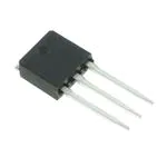
IPAK(TP)
1.2
2.3
SFT1452-TL-H
SFT1452-TL-W
1.2
4
7.0
5.5
4
2.3
6.5
5.0
1.5
0.5
7.0
SFT1452-H
SFT1452-W
2.3
6.5
5.0
2.3
1 : Gate
2 : Drain
3 : Source
4 : Drain
DPAK(TP-FA)
ORDERING INFORMATION
See detailed ordering and shipping information on page 2 of this data sheet.
Semiconductor Components Industries, LLC, 2014
June, 2014
60414HK TC-00003127/71112TKIM/41112TKIM PA No.9051-1/6
�SFT1452
Electrical Characteristics at Ta=25°C
Parameter
Symbol
Drain-to-Source Breakdown Voltage
Ratings
Conditions
Zero-Gate Voltage Drain Current
V(BR)DSS
IDSS
Gate-to-Source Leakage Current
IGSS
Gate Threshold Voltage
Forward Transconductance
VGS(th)
gFS
VDS=10V, ID=1.5A
Static Drain-to-Source On-State Resistance
RDS(on)
ID=1.5A, VGS=10V
Input Capacitance
Ciss
min
ID=1mA, VGS=0V
VDS=250V, VGS=0V
VGS=±24V, VDS=0V
250
VDS=10V, ID=1mA
2.5
typ
Unit
max
V
1
mA
±10
mA
4.5
1.7
1.8
V
S
2.4
W
210
pF
Output Capacitance
Coss
20
pF
Reverse Transfer Capacitance
Crss
7
pF
Turn-ON Delay Time
td(on)
8
ns
Rise Time
tr
9
ns
Turn-OFF Delay Time
td(off)
13
ns
Fall Time
Total Gate Charge
tf
Qg
Gate-to-Source Charge
Qgs
Gate-to-Drain “Miller” Charge
Qgd
Forward Diode Voltage
VSD
VDS=20V, f=1MHz
See specified Test Circuit.
VDS=125V, VGS=10V, ID=3A
14
ns
4.2
nC
1.4
nC
1.0
IS=3A, VGS=0V
0.95
nC
1.2
V
Product parametric performance is indicated in the Electrical Characteristics for the listed test conditions, unless otherwise noted. Product performance may not be
indicated by the Electrical Characteristics if operated under different conditions.
Switching Time Test Circuit
10V
0V
Electrical Connection
VDD=125V
VIN
2, 4
ID=1.5A
RL=81.3Ω
VIN
D
PW=10μs
D.C.≤1%
VOUT
1
G
3
SFT1452
P.G
50Ω
S
Ordering & Package Information
Device
Package
SFT1452-H
IPAK(TP)
SFT1452-W
SC-64, TO-251
SFT1452-TL-H
DAPK(TP-FA)
SFT1452-TL-W
SC-63, TO-252
Marking
Packing Type:TL
Shipping
memo
500pcs./bag
Pb-Free and Halogen Free
700pcs./reel
T1452
LOT No.
TL
No.9051-2/6
�SFT1452
ID -- VDS
2.0
1.5
5V
1.0
2
4
6
10
12
14
16
18
°C
--25
Ta=
25°C
75°C
3
2
1
RDS(on) -- VGS
HD6835
Single pulse
Ta=25°C
3
ID=1.5A
1
0
5
10
15
20
25
Gate-to-Source Voltage, VGS -- V
gFS -- ID
10
5
°C
-25
=
7
Ta
5
°C
75
3
5
6
7
8
100
120
9
10
140
160
HD6836
RDS(on) -- Ta
4
0V
3
1
S=
, VG
.5A
=1
ID
2
1
--40
--20
0
20
40
60
80
IS -- VSD
Single pulse
VGS=0V
3
2
HD16838
1.0
7
5
3
2
0.1
7
5
3
2
2
3
5 7 0.1
2
3
5 7 1.0
2
3
0.01
5 7 10
HD16839
Drain Current, ID -- A
SW Time -- ID
1000
7
5
2
Ciss, Coss, Crss -- pF
3
2
3
tf
td (off)
2
td(on)
10
7
5
tr
3
0.2
0.4
0.6
0.8
1.0
1.2
HD16840
Ciss, Coss, Crss -- VDS
1000
7
5
VDD=125V
VGS=10V
100
7
5
0
Forward Diode Voltage, VSD -- V
3
f=1MHz
Ciss
100
7
5
3
2
Coss
10
7
5
Crss
3
2
1.0
0.1
4
Single pulse
10
7
5
2
0.1
0.01
3
Gate-to-Source Voltage, VGS -- V
Ambient Temperature, Ta -- °C
Source Current, IS -- A
°C
25
1.0
2
HD16837
3
2
1
0
--60
30
Single pulse
VDS=10V
7
0
5
4
2
0
20
Static Drain-to-Source
On-State Resistance, RDS(on) -- Ω
Static Drain-to-Source
On-State Resistance, RDS(on) -- Ω
8
Drain-to-Source Voltage, VDS -- V
5
Forward Transconductance, gFS -- S
Single pulse
VDS=10V
Ta=7
5°C
25°C
--25°C
0
0
0
ID -- VGS(th)
VGS=4.5V
0.5
Switching Time, SW Time -- ns
Drain Current, ID -- A
6V
8V
Drain Current, ID -- A
2.5
4
Single pulse
10V
3.0
2
2
3
5
7
1.0
2
Drain Current, ID -- A
3
5
7
10
IT16841
1.0
0
10
20
30
40
50
60
70
80
Drain-to-Source Voltage, VDS -- V
90
100
IT16842
No.9051-3/6
�SFT1452
VGS -- Qg
10
8
10
7
5
7
3
2
5
3
2
0
0.5
1.0
1.5
2.0
2.5
3.0
3.5
Total Gate Charge, Qg -- nC
PD -- Ta
1.2
4.0
0.01
1.0
4.5
0.2
60
80
5
7 10
100
120
Ambient Temperature, Ta -- °C
140
2
3
5 7 100
PD -- Tc
2
3
HD16844
26
25
Power Dissipation, PD -- W
0.4
40
3
30
0.6
20
2
Drain-to-Source Voltage, VDS -- V
0.8
0
Tc=25°C
Single pulse
IT16843
1.0
0
n
tio
3
2
era
op
1
Operation in
this area is
limited by RDS(on).
DC
2
0
Power Dissipation, PD -- W
1.0
7
5
0.1
7
5
3
0μ
s
ID=3A
10
μs
s
4
10
s
1m s
m
10
6
IDP=12A(PW≤10μs)
0m
10
Drain Current, ID -- A
9
Gate-to-Source Voltage, VGS -- V
SOA
VDS=10V
ID=3A
20
15
10
5
0
160
HD16845
0
20
40
60
80
100
120
1
2
140
Case Temperature, Tc -- °C
160
HD16846
RθJC -- Pulse Time
10
Thermal Resistance, RθJC -- ºC/W
7
5
3
Duty Cycle=0.5
2
1.0
0.2
7
0.1
5
0.05
0.02
3
2
0.01
0.00001
le
ing
se
Pul
S
1
0.0
2
3
5
7 0.0001
2
3
5
7 0.001
2
3
5
7 0.01
2
Pulse Time, PT -- s
3
5
7 0.1
2
3
5
7
3
5 7 10
HD140512
No.9051-4/6
�SFT1452
Outline Drawing
SFT1452-TL-H, SFT1452-TL-W
Land Pattern Example
Mass (g) Unit
0.282 mm
* For reference
Unit: mm
7.0
7.0
2.5
2.0
1.5
2.3
2.3
No.9051-5/6
�SFT1452
Outline Drawing
SFT1452-H, SFT1452-W
Mass (g) Unit
0.315 mm
* For reference
Note on usage : Since the SFT1452 is a MOSFET product, please avoid using this device in the vicinity of
highly charged objects.
ON Semiconductor and the ON logo are registered trademarks of Semiconductor Components Industries, LLC (SCILLC). SCILLC owns the rights to a number
of patents, trademarks, copyrights, trade secrets, and other intellectual property. A listing of SCILLC’s product/patent coverage may be accessed at
www.onsemi.com/site/pdf/Patent-Marking.pdf. SCILLC reserves the right to make changes without further notice to any products herein. SCILLC makes no
warranty, representation or guarantee regarding the suitability of its products for any particular purpose, nor does SCILLC assume any liability arising out of the
application or use of any product or circuit, and specifically disclaims any and all liability, including without limitation special, consequential or incidental
damages. “Typical” parameters which may be provided in SCILLC data sheets and/or specifications can and do vary in different applications and actual
performance may vary over time. All operating parameters, including “Typicals” must be validated for each customer application by customer’s technical
experts. SCILLC does not convey any license under its patent rights nor the rights of others. SCILLC products are not designed, intended, or authorized for use
as components in systems intended for surgical implant into the body, or other applications intended to support or sustain life, or for any other application in
which the failure of the SCILLC product could create a situation where personal injury or death may occur. Should Buyer purchase or use SCILLC products for
any such unintended or unauthorized application, Buyer shall indemnify and hold SCILLC and its officers, employees, subsidiaries, affiliates, and distributors
harmless against all claims, costs, damages, and expenses, and reasonable attorney fees arising out of, directly or indirectly, any claim of personal injury or
death associated with such unintended or unauthorized use, even if such claim alleges that SCILLC was negligent regarding the design or manufacture of the
part. SCILLC is an Equal Opportunity/Affirmative Action Employer. This literature is subject to all applicable copyright laws and is not for resale in any manner.
PS No.9051-6/6
�