SG3525A
Pulse Width Modulator
Control Circuit
The SG3525A pulse width modulator control circuit offers
improved performance and lower external parts count when
implemented for controlling all types of switching power supplies.
The on−chip +5.1 V reference is trimmed to �1% and the error
amplifier has an input common−mode voltage range that includes the
reference voltage, thus eliminating the need for external divider
resistors. A sync input to the oscillator enables multiple units to be
slaved or a single unit to be synchronized to an external system clock.
A wide range of deadtime can be programmed by a single resistor
connected between the CT and Discharge pins. This device also
features built−in soft−start circuitry, requiring only an external timing
capacitor. A shutdown pin controls both the soft−start circuitry and the
output stages, providing instantaneous turn off through the PWM latch
with pulsed shutdown, as well as soft−start recycle with longer
shutdown commands. The under voltage lockout inhibits the outputs
and the changing of the soft−start capacitor when VCC is below
nominal. The output stages are totem−pole design capable of sinking
and sourcing in excess of 200 mA. The output stage of the SG3525A
features NOR logic resulting in a low output for an off−state.
http://onsemi.com
MARKING
DIAGRAMS
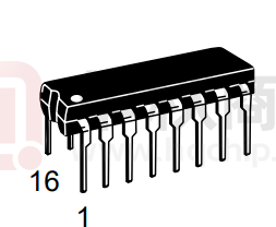
16
PDIP−16
N SUFFIX
CASE 648
SG3525AN
AWLYYWW
16
1
1
16
SOIC−16L
DW SUFFIX
CASE 751G
16
SG3525A
AWLYYWW
1
1
Features
•
•
•
•
•
•
•
•
•
•
A
WL
YY
WW
8.0 V to 35 V Operation
5.1 V � 1.0% Trimmed Reference
100 Hz to 400 kHz Oscillator Range
Separate Oscillator Sync Pin
Adjustable Deadtime Control
Input Undervoltage Lockout
Latching PWM to Prevent Multiple Pulses
Pulse−by−Pulse Shutdown
Dual Source/Sink Outputs: �400 mA Peak
Pb−Free Packages are Available*
= Assembly Location
= Wafer Lot
= Year
= Work Week
PIN CONNECTIONS
Inv. Input
1
16 Vref
Noninv. Input
2
15 VCC
Sync
3
14 Output B
OSC. Output
4
13 VC
CT
5
12 Ground
RT
6
11 Output A
Discharge
7
10 Shutdown
Soft−Start
8
9
Compensation
(Top View)
ORDERING INFORMATION
See detailed ordering and shipping information in the package
dimensions section on page 2 of this data sheet.
*For additional information on our Pb−Free strategy and soldering details, please
download the ON Semiconductor Soldering and Mounting Techniques
Reference Manual, SOLDERRM/D.
Semiconductor Components Industries, LLC, 2005
January, 2005 − Rev. 5
1
Publication Order Number:
SG3525A/D
�SG3525A
16
Vref
15
Reference
Regulator
VCC
12
VC
13
To Internal
Circuitry
Under−
Voltage
Lockout
Ground
OSC Output
NOR
4
3
Sync
RT
Output A
Q
6
F/F
Oscillator
Q
NOR
5
CT
Discharge
14
Output B
7
R
9
Compensation
11
1
INV. Input
2
Noninv. Input
−
Error
Amp
+
+
− PWM
−
S
Latch
SG3525A Output Stage
S
50�A
VREF
8
CSoft−Start
10
Shutdown
5.0k
5.0k
Figure 1. Representative Block Diagram
ORDERING INFORMATION
Package
Shipping†
SG3525AN
PDIP−16
25 Units / Rail
SG3525ANG
PDIP−16
(Pb−Free)
25 Units / Rail
SG3525ADW
SOIC−16L
47 Units / Rail
SG3525ADWG
SOIC−16L
(Pb−Free)
47 Units / Rail
SG3525ADWR2
SOIC−16L
1000 Tape & Reel
SG3525ADWR2G
SOIC−16L
(Pb−Free)
1000 Tape & Reel
Device
†For information on tape and reel specifications, including part orientation and tape sizes, please refer to our Tape and Reel Packaging
Specifications Brochure, BRD8011/D.
http://onsemi.com
2
�SG3525A
MAXIMUM RATINGS
Symbol
Value
Unit
Supply Voltage
Rating
VCC
+40
Vdc
Collector Supply Voltage
VC
+40
Vdc
Logic Inputs
−0.3 to +5.5
V
Analog Inputs
−0.3 to VCC
V
±500
mA
50
mA
5.0
mA
Output Current, Source or Sink
IO
Reference Output Current
Iref
Oscillator Charging Current
Power Dissipation
TA = +25°C (Note 1)
TC = +25°C (Note 2)
PD
mW
1000
2000
Thermal Resistance, Junction−to−Air
R�JA
100
°C/W
Thermal Resistance, Junction−to−Case
R�JC
60
°C/W
TJ
+150
°C
Tstg
−55 to +125
°C
TSolder
+300
°C
Operating Junction Temperature
Storage Temperature Range
Lead Temperature (Soldering, 10 seconds)
Maximum ratings are those values beyond which device damage can occur. Maximum ratings applied to the device are individual stress limit
values (not normal operating conditions) and are not valid simultaneously. If these limits are exceeded, device functional operation is not implied,
damage may occur and reliability may be affected.
1. Derate at 10 mW/°C for ambient temperatures above +50°C.
2. Derate at 16 mW/°C for case temperatures above +25°C.
RECOMMENDED OPERATING CONDITIONS
Characteristics
Symbol
Min
Max
Unit
Supply Voltage
VCC
8.0
35
Vdc
Collector Supply Voltage
VC
4.5
35
Vdc
Output Sink/Source Current
(Steady State)
(Peak)
IO
0
0
±100
±400
mA
Reference Load Current
Iref
0
20
mA
Oscillator Frequency Range
fosc
0.1
400
kHz
Oscillator Timing Resistor
RT
2.0
150
k�
Oscillator Timing Capacitor
CT
0.001
0.2
�F
Deadtime Resistor Range
RD
0
500
�
Operating Ambient Temperature Range
TA
0
+70
°C
APPLICATION INFORMATION
Shutdown Options (See Block Diagram, page 2)
latch is immediately set providing the fastest turn−off signal
to the outputs; and a 150 �A current sink begins to discharge
the external soft−start capacitor. If the shutdown command
is short, the PWM signal is terminated without significant
discharge of the soft−start capacitor, thus, allowing, for
example, a convenient implementation of pulse−by−pulse
current limiting. Holding Pin 10 high for a longer duration,
however, will ultimately discharge this external capacitor,
recycling slow turn−on upon release.
Pin 10 should not be left floating as noise pickup could
conceivably interrupt normal operation.
Since both the compensation and soft−start terminals
(Pins 9 and 8) have current source pull−ups, either can
readily accept a pull−down signal which only has to sink a
maximum of 100 �A to turn off the outputs. This is subject
to the added requirement of discharging whatever external
capacitance may be attached to these pins.
An alternate approach is the use of the shutdown circuitry
of Pin 10 which has been improved to enhance the available
shutdown options. Activating this circuit by applying a
positive signal on Pin 10 performs two functions: the PWM
http://onsemi.com
3
�SG3525A
ELECTRICAL CHARACTERISTICS (VCC = +20 Vdc, TA = Tlow to Thigh [Note 3], unless otherwise noted.)
Characteristics
Symbol
Min
Typ
Max
Unit
Reference Output Voltage (TJ = +25°C)
Vref
5.00
5.10
5.20
Vdc
Line Regulation (+8.0 V ≤ VCC ≤ +35 V)
Regline
−
10
20
mV
Load Regulation (0 mA ≤ IL ≤ 20 mA)
Regload
−
20
50
mV
Temperature Stability
�Vref/�T
−
20
−
mV
�Vref
4.95
−
5.25
Vdc
Short Circuit Current (Vref = 0 V, TJ = +25°C)
ISC
−
80
100
mA
Output Noise Voltage (10 Hz ≤ f ≤ 10 kHz, TJ = +25°C)
Vn
−
40
200
�Vrms
Long Term Stability (TJ = +125°C) (Note 4)
S
−
20
50
mV/khr
−
±2.0
±6.0
%
REFERENCE SECTION
Total Output Variation Includes Line and Load Regulation over Temperature
OSCILLATOR SECTION (Note 5, unless otherwise noted.)
Initial Accuracy (TJ = +25°C)
Frequency Stability with Voltage
(+8.0 V ≤ VCC ≤ +35 V)
�fosc
DVCC
−
±1.0
±2.0
%
Frequency Stability with Temperature
�fosc
DT
−
±0.3
−
%
Minimum Frequency (RT = 150 k�, CT = 0.2 �F)
fmin
−
50
−
Hz
Maximum Frequency (RT = 2.0 k�, CT = 1.0 nF)
fmax
400
−
−
kHz
Current Mirror (IRT = 2.0 mA)
1.7
2.0
2.2
mA
Clock Amplitude
3.0
3.5
−
V
Clock Width (TJ = +25°C)
0.3
0.5
1.0
�s
Sync Threshold
1.2
2.0
2.8
V
−
1.0
2.5
mA
Sync Input Current (Sync Voltage = +3.5 V)
ERROR AMPLIFIER SECTION (VCM = +5.1 V)
Input Offset Voltage
VIO
−
2.0
10
mV
Input Bias Current
IIB
−
1.0
10
�A
Input Offset Current
IIO
−
−
1.0
�A
DC Open Loop Gain (RL ≥ 10 M�)
AVOL
60
75
−
dB
Low Level Output Voltage
VOL
−
0.2
0.5
V
High Level Output Voltage
VOH
3.8
5.6
−
V
Common Mode Rejection Ratio (+1.5 V ≤ VCM ≤ +5.2 V)
CMRR
60
75
−
dB
Power Supply Rejection Ratio (+8.0 V ≤ VCC ≤ +35 V)
PSRR
50
60
−
dB
Minimum Duty Cycle
DCmin
−
−
0
%
Maximum Duty Cycle
DCmax
45
49
−
%
Input Threshold, Zero Duty Cycle (Note 5)
Vth
0.6
0.9
−
V
Input Threshold, Maximum Duty Cycle (Note 5)
Vth
−
3.3
3.6
V
Input Bias Current
IIB
−
0.05
1.0
�A
PWM COMPARATOR SECTION
3. Tlow = 0°
Thigh = +70°C
4. Since long term stability cannot be measured on each device before shipment, this specification is an engineering estimate of average
stability from lot to lot.
5. Tested at fosc = 40 kHz (RT = 3.6 k�, CT = 0.01 �F, RD = 0 �).
http://onsemi.com
4
�SG3525A
ELECTRICAL CHARACTERISTICS (continued)
Characteristics
Symbol
Min
Typ
Max
Unit
Soft−Start Current (Vshutdown = 0 V)
25
50
80
�A
Soft−Start Voltage (Vshutdown = 2.0 V)
−
0.4
0.6
V
Shutdown Input Current (Vshutdown = 2.5 V)
−
0.4
1.0
mA
−
−
0.2
1.0
0.4
2.0
18
17
19
18
−
−
7.0
8.0
V
SOFT−START SECTION
OUTPUT DRIVERS (Each Output, VCC = +20 V)
Output Low Level
(Isink = 20 mA)
(Isink = 100 mA)
VOL
Output High Level
(Isource = 20 mA)
(Isource = 100 mA)
VOH
Under Voltage Lockout (V8 and V9 = High)
VUL
6.0
V
V
IC(leak)
−
−
200
�A
Rise Time (CL = 1.0 nF, TJ = 25°C)
tr
−
100
600
ns
Fall Time (CL = 1.0 nF, TJ = 25°C)
tf
−
50
300
ns
Shutdown Delay (VDS = +3.0 V, CS = 0, TJ = +25°C)
tds
−
0.2
0.5
�s
Supply Current (VCC = +35 V)
ICC
−
14
20
mA
Collector Leakage, VC = +35 V (Note 6)
6. Applies to SG3525A only, due to polarity of output pulses.
Vref
16
4
PWM
ADJ.
13
Flip/
Flop
3
O
s
c
i
l
l
a
t
o
r
RT
6
Deadtime
1.5k
7
Ramp
0.009
100�
5
Out A
11
A
1.0k, 1.0W
(2)
14
B
0.001
0.1
VC
0.1
Sync
1.0k
VCC
0.1
0.1
Clock
3.0k
15
Reference Regulator
Out B
Comp
10k
1 = VIO
2 = 1(+)
3 = 1(−)
1
2
−
V/I Meter
+
12
PWM
GND
0.01
50�A
+
2
1
3
2
5.0�F
−
5.0k
E/A
5.0k
+
1
2
3
Softstart
8
1
3
1
2
3
9
10
Vref
2.0k
DUT
Shutdown
Figure 2. Lab Test Fixture
http://onsemi.com
5
�SG3525A
200
R D , DEAD TIME RESISTOR (�)
Ω
500
RT, TIMING RESISTOR (k Ω )
100
50
* RD = 0 �
20
10
5
6
5.0
RD *
RT
7
300
200
100
CT
2.0
0
2.0
5.0 10
20
50
100 200 500 1000 2000 5000 10,000
0.2
0.5
1.0
1
−
50
100 200
2
+
9
CP
RZ
RZ = 20 k
40
20
0
−20
1.0
10
100
1.0 k
10 k
100 k
1.0 M
4.0
3.5
2.5
2.0
1.5
Source Sat, (VC−VOH)
1.0
Sink Sat, (VOL)
0.5
0
0.01
10 M
VCC = +20 V
TJ = +25°C
3.0
f, FREQUENCY (Hz)
0.02 0.03 0.05 0.07 0.1
0.2 0.3
0.5 0.7 1.0
IO, OUTPUT SOURCE OR SINK CURRENT (A)
Figure 5. Error Amplifier Open Loop
Frequency Response
Figure 6. Output Saturation
Characteristics
15
16
VCC
Q5
Q1
Q8
7.4k
Q6
5
3
Sync
7
Discharge
Q2
Q3
Q3
6
12
GND
20
Figure 4. Oscillator Discharge Time versus RD
60
CT
10
Figure 3. Oscillator Charge Time versus RT
80
RT
5.0
DISCHARGE TIME (�s)
100
Vref
2.0
CHARGE TIME (�s)
V sat , SATURATION VOLTAGE (V)
A VOL, VOLTAGE GAIN (dB)
400
2.0k
Q9
2.0k
Ramp
To PWM
14k
Q11
Q10
25k
5.0pF
Blanking
Q14 To Output
400�A
Q4
23k
Q7
1.0k
1.0k
Q12
Q13
3.0k
Inverting
Q1
Input
1
Noninverting
Input
2
200�A
250
Q4
Q2
To PWM
Comparator
100�A
5.8V 30
9
Compensation
4
OSC Output
Figure 7. Oscillator Schematic
Figure 8. Error Amplifier Schematic
http://onsemi.com
6
�SG3525A
13
VCC
VC
Q7
Q5
Q9
Q10
Q4
5.0k
Vref
11, 14
Q11 Output
Q8
Q6
2.0k
Q1
Q2
5.0k
Clock
10k
Q3
Q6 Omitted
in SG3527A
10k
F/F
PWM
Figure 9. Output Circuit
(1/2 Circuit Shown)
Q1
+Vsupply
To Output Filter
+Vsupply
R1
R1
R2
VC A
13
VC
A
SG3525A
11
GND
Q2
R3
In conventional push−pull bipolar designs, forward base drive is
controlled by R1−R3. Rapid turn−off times for the power devices
are achieved with speed−up capacitors C1 and C2.
For single−ended supplies, the driver outputs are grounded.
The VC terminal is switched to ground by the totem−pole
source transistors on alternate oscillator cycles.
Figure 10. Single−Ended Supply
Figure 11. Push−Pull Configuration
+Vsupply
R1
Q1
11
Q1
14
C1
T1
T1
13
11
VC A
SG3525A
SG3525A
GND B
B
12
12
VC A
T1
Q1
R2
C2
14
14
GND
13
11
SG3525A
B
+Vsupply
C1
13
Q2
GND B
12
12
R1
T2
Q2
14
C2
R2
The low source impedance of the output drivers provides
rapid charging of power FET input capacitance while
minimizing external components.
Low power transformers can be driven directly by the SG3525A.
Automatic reset occurs during deadtime, when both ends of the
primary winding are switched to ground.
Figure 12. Driving Power FETS
Figure 13. Driving Transformers in a
Half−Bridge Configuration
http://onsemi.com
7
�MECHANICAL CASE OUTLINE
PACKAGE DIMENSIONS
PDIP−16
CASE 648−08
ISSUE V
16
1
SCALE 1:1
D
A
16
9
E
H
E1
1
NOTE 8
b2
8
c
B
TOP VIEW
END VIEW
WITH LEADS CONSTRAINED
NOTE 5
A2
A
e/2
NOTE 3
L
A1
C
D1
e
SEATING
PLANE
M
eB
END VIEW
16X b
SIDE VIEW
0.010
M
C A
M
B
M
NOTE 6
DATE 22 APR 2015
NOTES:
1. DIMENSIONING AND TOLERANCING PER ASME Y14.5M, 1994.
2. CONTROLLING DIMENSION: INCHES.
3. DIMENSIONS A, A1 AND L ARE MEASURED WITH THE PACKAGE SEATED IN JEDEC SEATING PLANE GAUGE GS−3.
4. DIMENSIONS D, D1 AND E1 DO NOT INCLUDE MOLD FLASH
OR PROTRUSIONS. MOLD FLASH OR PROTRUSIONS ARE
NOT TO EXCEED 0.10 INCH.
5. DIMENSION E IS MEASURED AT A POINT 0.015 BELOW DATUM
PLANE H WITH THE LEADS CONSTRAINED PERPENDICULAR
TO DATUM C.
6. DIMENSION eB IS MEASURED AT THE LEAD TIPS WITH THE
LEADS UNCONSTRAINED.
7. DATUM PLANE H IS COINCIDENT WITH THE BOTTOM OF THE
LEADS, WHERE THE LEADS EXIT THE BODY.
8. PACKAGE CONTOUR IS OPTIONAL (ROUNDED OR SQUARE
CORNERS).
DIM
A
A1
A2
b
b2
C
D
D1
E
E1
e
eB
L
M
INCHES
MIN
MAX
−−−−
0.210
0.015
−−−−
0.115 0.195
0.014 0.022
0.060 TYP
0.008 0.014
0.735 0.775
0.005
−−−−
0.300 0.325
0.240 0.280
0.100 BSC
−−−−
0.430
0.115 0.150
−−−−
10 °
MILLIMETERS
MIN
MAX
−−−
5.33
0.38
−−−
2.92
4.95
0.35
0.56
1.52 TYP
0.20
0.36
18.67 19.69
0.13
−−−
7.62
8.26
6.10
7.11
2.54 BSC
−−−
10.92
2.92
3.81
−−−
10 °
GENERIC
MARKING DIAGRAM*
16
STYLE 1:
PIN 1. CATHODE
2. CATHODE
3. CATHODE
4. CATHODE
5. CATHODE
6. CATHODE
7. CATHODE
8. CATHODE
9. ANODE
10. ANODE
11. ANODE
12. ANODE
13. ANODE
14. ANODE
15. ANODE
16. ANODE
DOCUMENT NUMBER:
DESCRIPTION:
STYLE 2:
PIN 1. COMMON DRAIN
2. COMMON DRAIN
3. COMMON DRAIN
4. COMMON DRAIN
5. COMMON DRAIN
6. COMMON DRAIN
7. COMMON DRAIN
8. COMMON DRAIN
9. GATE
10. SOURCE
11. GATE
12. SOURCE
13. GATE
14. SOURCE
15. GATE
16. SOURCE
98ASB42431B
PDIP−16
XXXXXXXXXXXX
XXXXXXXXXXXX
AWLYYWWG
1
XXXXX
A
WL
YY
WW
G
= Specific Device Code
= Assembly Location
= Wafer Lot
= Year
= Work Week
= Pb−Free Package
*This information is generic. Please refer to
device data sheet for actual part marking.
Pb−Free indicator, “G” or microdot “ G”,
may or may not be present.
Electronic versions are uncontrolled except when accessed directly from the Document Repository.
Printed versions are uncontrolled except when stamped “CONTROLLED COPY” in red.
PAGE 1 OF 1
ON Semiconductor and
are trademarks of Semiconductor Components Industries, LLC dba ON Semiconductor or its subsidiaries in the United States and/or other countries.
ON Semiconductor reserves the right to make changes without further notice to any products herein. ON Semiconductor makes no warranty, representation or guarantee regarding
the suitability of its products for any particular purpose, nor does ON Semiconductor assume any liability arising out of the application or use of any product or circuit, and specifically
disclaims any and all liability, including without limitation special, consequential or incidental damages. ON Semiconductor does not convey any license under its patent rights nor the
rights of others.
© Semiconductor Components Industries, LLC, 2019
www.onsemi.com
�MECHANICAL CASE OUTLINE
PACKAGE DIMENSIONS
SOIC−16 WB
CASE 751G
ISSUE E
1
SCALE 1:1
DATE 08 OCT 2021
GENERIC
MARKING DIAGRAM*
16
XXXXXXXXXXX
XXXXXXXXXXX
AWLYYWWG
1
XXXXX
A
WL
YY
WW
G
= Specific Device Code
= Assembly Location
= Wafer Lot
= Year
= Work Week
= Pb−Free Package
*This information is generic. Please refer to
device data sheet for actual part marking.
Pb−Free indicator, “G” or microdot “G”, may
or may not be present. Some products may
not follow the Generic Marking.
DOCUMENT NUMBER:
DESCRIPTION:
98ASB42567B
SOIC−16 WB
Electronic versions are uncontrolled except when accessed directly from the Document Repository.
Printed versions are uncontrolled except when stamped “CONTROLLED COPY” in red.
PAGE 1 OF 1
onsemi and
are trademarks of Semiconductor Components Industries, LLC dba onsemi or its subsidiaries in the United States and/or other countries. onsemi reserves
the right to make changes without further notice to any products herein. onsemi makes no warranty, representation or guarantee regarding the suitability of its products for any particular
purpose, nor does onsemi assume any liability arising out of the application or use of any product or circuit, and specifically disclaims any and all liability, including without limitation
special, consequential or incidental damages. onsemi does not convey any license under its patent rights nor the rights of others.
© Semiconductor Components Industries, LLC, 2019
www.onsemi.com
�onsemi,
, and other names, marks, and brands are registered and/or common law trademarks of Semiconductor Components Industries, LLC dba “onsemi” or its affiliates
and/or subsidiaries in the United States and/or other countries. onsemi owns the rights to a number of patents, trademarks, copyrights, trade secrets, and other intellectual property.
A listing of onsemi’s product/patent coverage may be accessed at www.onsemi.com/site/pdf/Patent−Marking.pdf. onsemi reserves the right to make changes at any time to any
products or information herein, without notice. The information herein is provided “as−is” and onsemi makes no warranty, representation or guarantee regarding the accuracy of the
information, product features, availability, functionality, or suitability of its products for any particular purpose, nor does onsemi assume any liability arising out of the application or use
of any product or circuit, and specifically disclaims any and all liability, including without limitation special, consequential or incidental damages. Buyer is responsible for its products
and applications using onsemi products, including compliance with all laws, regulations and safety requirements or standards, regardless of any support or applications information
provided by onsemi. “Typical” parameters which may be provided in onsemi data sheets and/or specifications can and do vary in different applications and actual performance may
vary over time. All operating parameters, including “Typicals” must be validated for each customer application by customer’s technical experts. onsemi does not convey any license
under any of its intellectual property rights nor the rights of others. onsemi products are not designed, intended, or authorized for use as a critical component in life support systems
or any FDA Class 3 medical devices or medical devices with a same or similar classification in a foreign jurisdiction or any devices intended for implantation in the human body. Should
Buyer purchase or use onsemi products for any such unintended or unauthorized application, Buyer shall indemnify and hold onsemi and its officers, employees, subsidiaries, affiliates,
and distributors harmless against all claims, costs, damages, and expenses, and reasonable attorney fees arising out of, directly or indirectly, any claim of personal injury or death
associated with such unintended or unauthorized use, even if such claim alleges that onsemi was negligent regarding the design or manufacture of the part. onsemi is an Equal
Opportunity/Affirmative Action Employer. This literature is subject to all applicable copyright laws and is not for resale in any manner.
PUBLICATION ORDERING INFORMATION
LITERATURE FULFILLMENT:
Email Requests to: orderlit@onsemi.com
onsemi Website: www.onsemi.com
◊
TECHNICAL SUPPORT
North American Technical Support:
Voice Mail: 1 800−282−9855 Toll Free USA/Canada
Phone: 011 421 33 790 2910
Europe, Middle East and Africa Technical Support:
Phone: 00421 33 790 2910
For additional information, please contact your local Sales Representative
�