Is Now Part of
To learn more about ON Semiconductor, please visit our website at
www.onsemi.com
Please note: As part of the Fairchild Semiconductor integration, some of the Fairchild orderable part numbers
will need to change in order to meet ON Semiconductor’s system requirements. Since the ON Semiconductor
product management systems do not have the ability to manage part nomenclature that utilizes an underscore
(_), the underscore (_) in the Fairchild part numbers will be changed to a dash (-). This document may contain
device numbers with an underscore (_). Please check the ON Semiconductor website to verify the updated
device numbers. The most current and up-to-date ordering information can be found at www.onsemi.com. Please
email any questions regarding the system integration to Fairchild_questions@onsemi.com.
ON Semiconductor and the ON Semiconductor logo are trademarks of Semiconductor Components Industries, LLC dba ON Semiconductor or its subsidiaries in the United States and/or other countries. ON Semiconductor owns the rights to a number
of patents, trademarks, copyrights, trade secrets, and other intellectual property. A listing of ON Semiconductor’s product/patent coverage may be accessed at www.onsemi.com/site/pdf/Patent-Marking.pdf. ON Semiconductor reserves the right
to make changes without further notice to any products herein. ON Semiconductor makes no warranty, representation or guarantee regarding the suitability of its products for any particular purpose, nor does ON Semiconductor assume any liability
arising out of the application or use of any product or circuit, and specifically disclaims any and all liability, including without limitation special, consequential or incidental damages. Buyer is responsible for its products and applications using ON
Semiconductor products, including compliance with all laws, regulations and safety requirements or standards, regardless of any support or applications information provided by ON Semiconductor. “Typical” parameters which may be provided in ON
Semiconductor data sheets and/or specifications can and do vary in different applications and actual performance may vary over time. All operating parameters, including “Typicals” must be validated for each customer application by customer’s
technical experts. ON Semiconductor does not convey any license under its patent rights nor the rights of others. ON Semiconductor products are not designed, intended, or authorized for use as a critical component in life support systems or any FDA
Class 3 medical devices or medical devices with a same or similar classification in a foreign jurisdiction or any devices intended for implantation in the human body. Should Buyer purchase or use ON Semiconductor products for any such unintended
or unauthorized application, Buyer shall indemnify and hold ON Semiconductor and its officers, employees, subsidiaries, affiliates, and distributors harmless against all claims, costs, damages, and expenses, and reasonable attorney fees arising out
of, directly or indirectly, any claim of personal injury or death associated with such unintended or unauthorized use, even if such claim alleges that ON Semiconductor was negligent regarding the design or manufacture of the part. ON Semiconductor
is an Equal Opportunity/Affirmative Action Employer. This literature is subject to all applicable copyright laws and is not for resale in any manner.
�SGH30N60RUFD
Short Circuit Rated IGBT
General Description
Features
Fairchild's RUFD series of Insulated Gate Bipolar
Transistors (IGBTs) provide low conduction and switching
losses as well as short circuit ruggedness. The RUFD
series is designed for applications such as motor control,
uninterrupted power supplies (UPS) and general inverters
where short circuit ruggedness is a required feature.
•
•
•
•
•
Short circuit rated 10us @ TC = 100°C, VGE = 15V
High speed switching
Low saturation voltage : VCE(sat) = 2.2 V @ IC = 30A
High input impedance
CO-PAK, IGBT with FRD : trr = 50ns (typ.)
Applications
AC & DC motor controls, general purpose inverters, robotics, and servo controls.
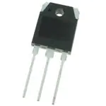
C
G
TO-3PN
E
G C E
Absolute Maximum Ratings
Symbol
VCES
VGES
IC
ICM (1)
IF
IFM
TSC
PD
TJ
Tstg
TL
TC = 25°C unless otherwise noted
Description
Collector-Emitter Voltage
Gate-Emitter Voltage
Collector Current
Collector Current
Pulsed Collector Current
Diode Continuous Forward Current
Diode Maximum Forward Current
Short Circuit Withstand Time
Maximum Power Dissipation
Maximum Power Dissipation
Operating Junction Temperature
Storage Temperature Range
Maximum Lead Temp. for Soldering
Purposes, 1/8” from Case for 5 Seconds
@ TC = 25°C
@ TC = 100°C
@ TC = 100°C
@ TC =100°C
@ TC = 25°C
@ TC = 100°C
SGH30N60RUFD
600
± 20
48
30
90
25
220
10
235
90
-55 to +150
-55 to +150
Units
V
V
A
A
A
A
A
us
W
W
°C
°C
300
°C
Notes :
(1) Repetitive rating : Pulse width limited by max. junction temperature
Thermal Characteristics
Symbol
RθJC(IGBT)
RθJC(DIODE)
RθJA
Parameter
Thermal Resistance, Junction-to-Case
Thermal Resistance, Junction-to-Case
Thermal Resistance, Junction-to-Ambient
©2002 Fairchild Semiconductor Corporation
Typ.
----
Max.
0.53
0.83
40
Units
°C/W
°C/W
°C/W
SGH30N60RUFD Rev. B1
SGH30N60RUFD
IGBT
�C
Symbol
Parameter
= 25°C unless otherwise noted
Test Conditions
Min.
Typ.
Max.
Units
600
--
--
V
VGE = 0V, IC = 1mA
--
0.6
--
V/°C
VCE = VCES, VGE = 0V
VGE = VGES, VCE = 0V
---
---
250
± 100
uA
nA
IC = 30mA, VCE = VGE
IC = 30A, VGE = 15V
IC = 48A, VGE = 15V
5.0
---
6.0
2.2
2.5
8.5
2.8
--
V
V
V
----
1970
310
74
----
pF
pF
pF
---------------
30
65
54
138
919
814
1733
34
67
60
281
921
1556
2477
--80
200
--2430
--90
400
--3470
ns
ns
ns
ns
uJ
uJ
uJ
ns
ns
ns
ns
uJ
uJ
uJ
Off Characteristics
BVCES
∆BVCES/
∆TJ
ICES
IGES
Collector-Emitter Breakdown Voltage
Temperature Coefficient of Breakdown
Voltage
Collector Cut-Off Current
G-E Leakage Current
VGE = 0V, IC = 250uA
On Characteristics
VGE(th)
VCE(sat)
G-E Threshold Voltage
Collector to Emitter
Saturation Voltage
Dynamic Characteristics
Cies
Coes
Cres
Input Capacitance
Output Capacitance
Reverse Transfer Capacitance
VCE = 30V, VGE = 0V,
f = 1MHz
Switching Characteristics
td(on)
tr
td(off)
tf
Eon
Eoff
Ets
td(on)
tr
td(off)
tf
Eon
Eoff
Ets
Turn-On Delay Time
Rise Time
Turn-Off Delay Time
Fall Time
Turn-On Switching Loss
Turn-Off Switching Loss
Total Switching Loss
Turn-On Delay Time
Rise Time
Turn-Off Delay Time
Fall Time
Turn-On Switching Loss
Turn-Off Switching Loss
Total Switching Loss
Tsc
Short Circuit Withstand Time
Qg
Qge
Qgc
Le
Total Gate Charge
Gate-Emitter Charge
Gate-Collector Charge
Internal Emitter Inductance
VCC = 300 V, IC = 30A,
RG = 7Ω, VGE = 15V,
Inductive Load, TC = 25°C
VCC = 300 V, IC = 30A,
RG = 7Ω, VGE = 15V,
Inductive Load, TC = 125°C
VCC = 300 V, VGE = 15V
100°C
VFM
Diode Forward Voltage
trr
Diode Reverse Recovery Time
Irr
Diode Peak Reverse Recovery
Current
Qrr
Diode Reverse Recovery Charge
©2002 Fairchild Semiconductor Corporation
--
us
85
17
39
14
120
25
55
--
nC
nC
nC
nH
Min.
--
Typ.
1.4
Max.
1.7
Units
--
1.3
--
TC = 25°C
--
50
95
TC = 100°C
--
105
--
TC = 25°C
--
4.5
10
TC = 100°C
--
8.5
--
TC = 25°C
--
112
375
TC = 100°C
--
420
--
Measured 5mm from PKG
C
Parameter
--
-----
VCE = 300 V, IC = 30A,
VGE = 15V
Electrical Characteristics of DIODE T
Symbol
10
@ TC =
= 25°C unless otherwise noted
Test Conditions
TC = 25°C
IF = 25A
TC = 100°C
IF= 25A,
di/dt = 200 A/us
V
ns
A
nC
SGH30N60RUFD Rev. B1
SGH30N60RUFD
Electrical Characteristics of the IGBT T
�20V
15V
70
Collector Current, IC [A]
Common Emitter
VGE = 15V
T C = 25℃ ━━
T C = 125℃ ------
80
Collector Current, IC [A]
Common Emitter
TC = 25℃
80
60
12V
50
40
30
VGE = 10V
70
60
50
40
30
20
20
10
10
0
0
0
2
4
6
1
8
Collector - Emitter Voltage, VCE [V]
10
Collector - Emitter Voltage, VCE [V]
Fig 1. Typical Output Characteristics
Fig 2. Typical Saturation Voltage Characteristics
5
40
Common Emitter
V GE = 15V
VCC = 300V
Load Current : peak of square wave
35
60A
4
30
45A
3
30A
2
IC = 15A
Load Current [A]
Collector - Emitter Voltage, V CE [V]
SGH30N60RUFD
90
90
25
20
15
10
1
Duty cycle : 50%
TC = 100℃
Power Dissipation = 45W
5
0
0
-50
0
50
100
0.1
150
1
10
Fig 3. Saturation Voltage vs. Case
Temperature at Variant Current Level
1000
Fig 4. Load Current vs. Frequency
20
20
Common Emitter
T C = 25℃
Common Emitter
T C = 125℃
Collector - Emitter Voltage, VCE [V]
Collector - Emitter Voltage, VCE [V]
100
Frequency [KHz]
Case Temperature, T C [℃]
16
12
8
4
30A
60A
16
12
8
60A
4
30A
IC = 15A
IC = 15A
0
0
4
8
12
16
Gate - Emitter Voltage, V GE [V]
Fig 5. Saturation Voltage vs. VGE
©2002 Fairchild Semiconductor Corporation
20
4
8
12
16
20
Gate - Emitter Voltage, VGE [V]
Fig 6. Saturation Voltage vs. VGE
SGH30N60RUFD Rev. B1
�Common Emitter
VGE = 0V, f = 1MHz
TC = 25℃
3000
Common Emitter
VCC = 300V, VGE = ± 15V
IC = 30A
T C = 25℃ ━━
T C = 125℃ ------
Cies
2500
Switching Time [ns]
Capacitance [pF]
SGH30N60RUFD
1000
3500
2000
Coes
1500
1000
Ton
Tr
100
Cres
500
10
0
1
1
10
10
Fig 8. Turn-On Characteristics vs.
Gate Resistance
Fig 7. Capacitance Characteristics
10000
Common Emitter
V CC = 300V, V GE = ± 15V
IC = 30A
T C = 25℃ ━━
T C = 125℃ ------
Common Emitter
V CC = 300V, VGE = ± 15V
IC = 30A
T C = 25℃ ━━
T C = 125℃ ------
Switching Loss [uJ]
Switching Time [ns]
1000
100
Gate Resistance, RG [Ω ]
Collector - Emitter Voltage, V CE [V]
Toff
Toff
Tf
Eon
Eoff
1000
Eoff
Tf
100
100
1
10
1
100
10
Gate Resistance, R G [Ω ]
Fig 9. Turn-Off Characteristics vs.
Gate Resistance
Fig 10. Switching Loss vs. Gate Resistance
1000
1000
Common Emitter
V GE = ± 15V, RG = 7Ω
T C = 25℃ ━━
T C = 125℃ ------
Switching Time [ns]
Common Emitter
V GE = ± 15V, RG = 7 Ω
T C = 25℃ ━━
T C = 125℃ ------
Switching Time [ns]
100
Gate Resistance, R G [ Ω ]
Ton
Tr
100
Toff
Tf
Toff
100
Tf
10
15
30
45
Collector Current, IC [A]
Fig 11. Turn-On Characteristics vs.
Collector Current
©2002 Fairchild Semiconductor Corporation
60
15
30
45
60
Collector Current, IC [A]
Fig 12. Turn-Off Characteristics vs.
Collector Current
SGH30N60RUFD Rev. B1
�15
Gate - Emitter Voltage, VGE [ V ]
Common Emitter
VGE = ± 15V, RG = 7 Ω
TC = 25℃ ━━
TC = 125℃ ------
Switching Loss [uJ]
SGH30N60RUFD
10000
Eoff
Eon
Eoff
1000
100
Common Emitter
RL = 10 Ω
TC = 25℃
12
300 V
V CC = 100 V
200 V
9
6
3
0
15
30
45
60
0
20
Collector Current, IC [A]
40
60
80
100
Gate Charge, Qg [ nC ]
Fig 13. Switching Loss vs. Collector Current
Fig 14. Gate Charge Characteristics
200
100
IC MAX. (Pulsed)
100
50us
100us
Collector Current, IC [A]
Collector Current, IC [A]
IC MAX. (Continuous)
1㎳
10
DC Operation
1
Single Nonrepetitive
Pulse TC = 25℃
Curves must be derated
linearly with increase
in temperature
Safe Operating Area
VGE = 20V, T C = 100℃
0.1
0.3
10
1
10
100
1
1000
1
10
Fig 15. SOA Characteristics
Thermal Response, Zthjc [℃/W]
100
1000
Collector-Emitter Voltage, V CE [V]
Collector-Emitter Voltage, V CE [V]
Fig 16. Turn-Off SOA Characteristics
1
0.5
0.2
0.1
0.1
0.05
0.02
0.01
Pdm
0.01
t1
t2
single pulse
Duty factor D = t1 / t2
Peak Tj = Pdm × Zthjc + TC
1E-3
10
-5
10
-4
-3
10
10
-2
10
-1
0
10
10
1
Rectangular Pulse Duration [sec]
Fig 17. Transient Thermal Impedance of IGBT
©2002 Fairchild Semiconductor Corporation
SGH30N60RUFD Rev. B1
�SGH30N60RUFD
100
T C = 25℃ ━━
T C = 100℃ ------
Reverse Recovery Current, Irr [A]
Forward Current, IF [A]
100
10
1
2
10
1
100
1
0
VR = 200V
IF = 25A
T C = 25℃ ━━
T C = 100℃ ------
3
Fig 18. Forward Characteristics
Fig 19. Reverse Recovery Current
120
1000
V R = 200V
IF = 25A
T C = 25℃ ━━
T C = 100℃ ------
800
Reverce Recovery Time, t rr [ns]
Stored Recovery Charge, Qrr [nC]
1000
di/dt [A/us]
Forward Voltage Drop, VFM [V]
600
400
200
0
100
1000
di/dt [A/us]
Fig 20. Stored Charge
©2002 Fairchild Semiconductor Corporation
V R = 200V
IF = 25A
T C = 25℃ ━━
T C = 100℃ ------
100
80
60
40
20
100
1000
di/dt [A/us]
Fig 21. Reverse Recovery Time
SGH30N60RUFD Rev. B1
�SGH30N60RUFD
Mechanical Dimensions
TO-3PN
Dimensions in Millimeters
©2002 Fairchild Semiconductor Corporation
SGH30N60RUFD Rev. B1
�TRADEMARKS
The following are registered and unregistered trademarks Fairchild Semiconductor owns or is authorized to use and is
not intended to be an exhaustive list of all such trademarks.
ACEx
FACT
ActiveArray
FACT Quiet Series
Bottomless
FASTâ
CoolFET
FASTr
CROSSVOLT FRFET
DOME
GlobalOptoisolator
EcoSPARK
GTO
E2CMOSTM
HiSeC
EnSignaTM
I2C
Across the board. Around the world.
The Power Franchise
Programmable Active Droop
ImpliedDisconnect PACMAN
POP
ISOPLANAR
Power247
LittleFET
PowerTrenchâ
MicroFET
QFET
MicroPak
QS
MICROWIRE
QT Optoelectronics
MSX
Quiet Series
MSXPro
RapidConfigure
OCX
RapidConnect
OCXPro
SILENT SWITCHERâ
OPTOLOGICâ
SMART START
OPTOPLANAR
SPM
Stealth
SuperSOT-3
SuperSOT-6
SuperSOT-8
SyncFET
TinyLogic
TruTranslation
UHC
UltraFETâ
VCX
DISCLAIMER
FAIRCHILD SEMICONDUCTOR RESERVES THE RIGHT TO MAKE CHANGES WITHOUT FURTHER
NOTICE TO ANY PRODUCTS HEREIN TO IMPROVE RELIABILITY, FUNCTION OR DESIGN. FAIRCHILD
DOES NOT ASSUME ANY LIABILITY ARISING OUT OF THE APPLICATION OR USE OF ANY PRODUCT
OR CIRCUIT DESCRIBED HEREIN; NEITHER DOES IT CONVEY ANY LICENSE UNDER ITS PATENT
RIGHTS, NOR THE RIGHTS OF OTHERS.
LIFE SUPPORT POLICY
FAIRCHILDS PRODUCTS ARE NOT AUTHORIZED FOR USE AS CRITICAL COMPONENTS IN LIFE SUPPORT
DEVICES OR SYSTEMS WITHOUT THE EXPRESS WRITTEN APPROVAL OF FAIRCHILD SEMICONDUCTOR CORPORATION.
As used herein:
2. A critical component is any component of a life
1. Life support devices or systems are devices or
support device or system whose failure to perform can
systems which, (a) are intended for surgical implant into
be reasonably expected to cause the failure of the life
the body, or (b) support or sustain life, or (c) whose
support device or system, or to affect its safety or
failure to perform when properly used in accordance
with instructions for use provided in the labeling, can be
effectiveness.
reasonably expected to result in significant injury to the
user.
PRODUCT STATUS DEFINITIONS
Definition of Terms
Datasheet Identification
Product Status
Definition
Advance Information
Formative or
In Design
This datasheet contains the design specifications for
product development. Specifications may change in
any manner without notice.
Preliminary
First Production
This datasheet contains preliminary data, and
supplementary data will be published at a later date.
Fairchild Semiconductor reserves the right to make
changes at any time without notice in order to improve
design.
No Identification Needed
Full Production
This datasheet contains final specifications. Fairchild
Semiconductor reserves the right to make changes at
any time without notice in order to improve design.
Obsolete
Not In Production
This datasheet contains specifications on a product
that has been discontinued by Fairchild semiconductor.
The datasheet is printed for reference information only.
Rev. I1
�ON Semiconductor and
are trademarks of Semiconductor Components Industries, LLC dba ON Semiconductor or its subsidiaries in the United States and/or other countries.
ON Semiconductor owns the rights to a number of patents, trademarks, copyrights, trade secrets, and other intellectual property. A listing of ON Semiconductor’s product/patent
coverage may be accessed at www.onsemi.com/site/pdf/Patent−Marking.pdf. ON Semiconductor reserves the right to make changes without further notice to any products herein.
ON Semiconductor makes no warranty, representation or guarantee regarding the suitability of its products for any particular purpose, nor does ON Semiconductor assume any liability
arising out of the application or use of any product or circuit, and specifically disclaims any and all liability, including without limitation special, consequential or incidental damages.
Buyer is responsible for its products and applications using ON Semiconductor products, including compliance with all laws, regulations and safety requirements or standards,
regardless of any support or applications information provided by ON Semiconductor. “Typical” parameters which may be provided in ON Semiconductor data sheets and/or
specifications can and do vary in different applications and actual performance may vary over time. All operating parameters, including “Typicals” must be validated for each customer
application by customer’s technical experts. ON Semiconductor does not convey any license under its patent rights nor the rights of others. ON Semiconductor products are not
designed, intended, or authorized for use as a critical component in life support systems or any FDA Class 3 medical devices or medical devices with a same or similar classification
in a foreign jurisdiction or any devices intended for implantation in the human body. Should Buyer purchase or use ON Semiconductor products for any such unintended or unauthorized
application, Buyer shall indemnify and hold ON Semiconductor and its officers, employees, subsidiaries, affiliates, and distributors harmless against all claims, costs, damages, and
expenses, and reasonable attorney fees arising out of, directly or indirectly, any claim of personal injury or death associated with such unintended or unauthorized use, even if such
claim alleges that ON Semiconductor was negligent regarding the design or manufacture of the part. ON Semiconductor is an Equal Opportunity/Affirmative Action Employer. This
literature is subject to all applicable copyright laws and is not for resale in any manner.
PUBLICATION ORDERING INFORMATION
LITERATURE FULFILLMENT:
Literature Distribution Center for ON Semiconductor
19521 E. 32nd Pkwy, Aurora, Colorado 80011 USA
Phone: 303−675−2175 or 800−344−3860 Toll Free USA/Canada
Fax: 303−675−2176 or 800−344−3867 Toll Free USA/Canada
Email: orderlit@onsemi.com
© Semiconductor Components Industries, LLC
N. American Technical Support: 800−282−9855 Toll Free
USA/Canada
Europe, Middle East and Africa Technical Support:
Phone: 421 33 790 2910
Japan Customer Focus Center
Phone: 81−3−5817−1050
www.onsemi.com
1
ON Semiconductor Website: www.onsemi.com
Order Literature: http://www.onsemi.com/orderlit
For additional information, please contact your local
Sales Representative
www.onsemi.com
�